SMCJ5351中文资料
SMC气缸第一册(执行元件)E
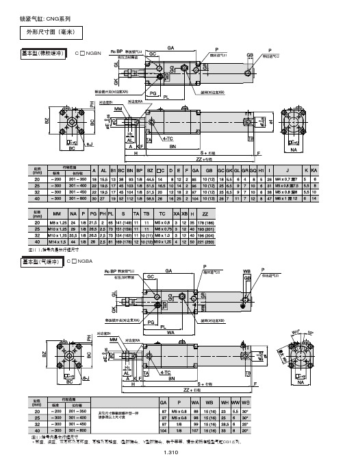
注1) 脚座安装及杆侧法兰安装最长行程可至1400mm。铁缸筒最长行程可 至1600mm。 注2) 磁性开关规格及特性可参阅磁性开关的系列。在磁性开关型号的后面, 附导线长度记号:无记号:-0.5m,L-3m,Z-5m,例:Z73L 注3) 所有磁性开关只适用于铝缸筒。
外形尺寸图 (毫米)
* 脚座、法兰、双耳环及耳环座、轴耳及 轴耳座、I 型肘接头、Y 型肘接头、销子 等等,请参阅标准型气缸 CS1 系列。
160
型号表示方法 基本型:
注)
*不能使用磁性开关。
CNS
基本型
B
125 160
100 500
行程
D D
双向锁
带磁性开关 0℃~60℃,不带磁性开关 0℃~70℃ 50~500mm/s 气缓冲
~ 250: 0 , 251 ~ 1000: 0 , 1001 ~ 1500: 0 , 1501 ~ 1600: 0
43 11.2 52 11.2 52 11.2 65 12.5 65 14
1.313
!L
!
CNS
(ø125
缸筒材质 无记号 铝 铁 *F
ø160)
标准规格
缸径(mm) 使用流体 动作方式 最高使用压力 最低使用压力 环境和流体温度 活塞速度 缓冲 行程公差(mm)
+1.0
125
140 空气 双作用 0.97MPa 0.08MPa
J
M8×1.25 M8×1.25 M10×1.25 M12×1.75 M12×1.75
K
6 7 7 11 11
KA
14 18 18 22 26
40 50 63 80 100
缸径 (mm)
带防护套
11548附件: 合金技术条件 本标准规定了铝镍钴永磁合金的材料牌号、主要磁性能的最低值、尺寸和形
纸浆模塑工业包装制品
本标准规定了纸浆模塑工业包装制品生产线的术语和定
生产线
义、型号、型式与基本参数、技术要求、试验方法、检验规
则及标志、包装、运输和贮存等要求。
本标准适用于贮存与运输时直接包装各种工业制品及电
子产品的纸浆模塑工业包装制品(不含模具内干燥的制品)
采标情况
序 标准编号
号 9 JB/T 12106-2014
本标准不适用于空心轴磁轭锻件。
汽轮机、汽轮发电机转
本标准对汽轮机、汽轮发电机转子和主轴锻件超声检测 JB/T 1581-1996
子和主轴锻件超声检测 的检测人员、检测器材、操作要领和检测结果记录评定等内
方法
容作了规定。
本标准适用于直径为2500mm以下的各类转子和主轴锻件
的超声检测。其他各种工况条件类似的轴类锻件可参考使用
明书、标志和包装等。
本标准适用于300MW以上汽轮机缸体铸钢件的订货、制
造、检验和验收。
汽 轮 发 电 机 Mn18Cr18N
本标准规定了汽轮发电机1Mn18Cr18N无磁性护环锻件的 JB/T 7030-2002
无磁性护环锻件 技术 订货要求、制造工艺、技术要求、检验规则和试验方法、质 JB/T 1268-2002
标准名称
标准主要内容
代替标准
50MW以下汽轮发电机无
本标准规定了50MW以下汽轮发电机无中心孔转子锻件的 JB/T 8705-1998
中心孔转子锻件 技术 订货要求、制造工艺、技术要求、检验规则和试验方法、验
条件
收和质量证明书及标志和包装等。
本标准适用于50MW以下汽轮发电机无中心孔转子锻件的
订货、制造与检验。
本部分规定了采用碘量法测定铜钨电触头材料中铜含量 -1999
SMC书本资料

标准型(通孔):CDQ2BP□-□DM-□□
二面宽 K
通孔 沉孔
±0.2
行程 行程
※气缸带金属防尘圈
两端螺孔的场合 缸径 O (mm) 50 63 80 标准型 缸径 (mm) 50 63 80 A B C D E F H M8X1.25 M10X1.5 M12X1.75
两端螺孔 CDQ2AP □ - □ DM- □□
IB 47 58 72
N 52 49 49
W 5 7 5.5
WC 34 38 44
WS 44 39 45
S 65 58 58
Z 90 80 80
ZZ 204 194 194
Hs 45 49 54.5
Ht 28 28 28
注)附件尺寸图参见P1.95
1.101
!: CDQ2 !"=E
P F
2-RcP
行程
无杆侧法兰型:CDA1GP□-□□-□□
杆侧法兰型 缸径 40 50 63 80
B 71 81 101 119
FV 60 70 86 102
FD 9.0 9.0 11.5 13.5
FT 12 12 15 18
FX 80 90 105 130
FY 42 50 59 76
FZ 100 110 130 160
ZZ 190 210 227 270
中间耳轴型:CDA1TP□-□□-□□
Z+1/2 行程
行程
中间耳轴型 缸径 40 50 63 80
行程范围
带 1 个、 带2个
TDe8 15 15 18 25
-0.032 -0.059 -0.032 -0.059 -0.032 -0.059 -0.040 -0.073
通变电器有限公司宣传手册

目录CONTENTS预装式变电站系列XGW2-40.5(12)………………………………………………P001 YBW11-12 / 0.4-□………………………………………………P002 10kV级系列开关柜KYN28A-12 ………………………………………………………P003 XGN2-12(Z) ………………………………………………………P004 XGN15-12 ………………………………………………………P005 35kV级系列开关柜KYN61-40.5…………………………………………………………P006 GBC-35 …………………………………………………………P007 0.4kV级系列开关柜GCS ……………………………………………………………P008 MNS ………………………………………………………………P009 GGD ………………………………………………………………P010 JP ………………………………………………………………P011 XL-21 ………………………………………………………………P012XGW2-40.5(12)智能型(四遥)箱式移动开关站●概述XGW2-40.5(12)智能型(四遥)箱式移动开关站,是将40.5kV或12kV一、二次配电设备在工厂内装于一个可移动、全封闭、恒温、防潮、防锈的箱体内。
开关站由箱体、各单元开关柜、主母线、操作走廊、空调、后台机等组成。
进线方式为电缆进线或架空进线。
单元开关柜布置形式:单列布置或双列布置。
接线类别:单母线分段、单母线不分段、双进线联络。
通风形式:恒温空调。
●结构➢箱体箱体的结构由槽钢、角钢、厚钢板焊接而成,表面防腐喷涂处理,以保证长时间不锈蚀,各单元间隔的门和防护板及顶板均为优质彩钢夹芯复合板,具有结构坚固、隔温、防锈、防潮、绝缘性能好、重量轻等优点。
➢单元开关柜各单元间隔采用单元柜结构形式,一、二次元器件均装于单元开关柜中。
第一卷第1册第01篇 J5AIS1 说明书+清册

南方电网变电站标准设计第一卷 500kV 变电站标准设计第一册 500kV 配电装置模块第一篇 CSG-500B-J5AIS1模块南方电网公司 2010年12月2011年版第一章:设计说明目录1总的部分 (1)1.1 模块建设规模 (1)1.2 模块的特点和适用范围 (1)1.3 模块与南网标准设计方案(2006版)的差异 (1)1.4 模块绿色设计原则 (1)1.5 模块使用边界条件 (1)1.6 模块的电气二次部分 (2)1.7 模块的建构筑物 (2)1.8 本模块主要技术经济指标 (2)2电气一次部分 (3)2.1 电气接线 (3)2.2 主要设备和导体选择 (3)2.3 绝缘配合及过电压保护和接地 (4)2.4 配电装置及平面布置 (5)2.5 站用电及照明 (5)2.6 电缆设施 (5)3电气二次部分 (6)3.1 综合自动化系统 (6)3.2 保护及录波配置 (6)3.3 公用系统 (6)4土建部分 (6)4.1 模块总体布置 (6)4.2 建筑设计 (6)4.3 结构设计 (7)4.4 水工 (7)1 总的部分1.1 模块建设规模CSG-500B-J5AIS1为500kV变电站500kV配电装置模块之一, 其建设规模见表1-1-1。
本模块按照终期规模建设设计,通过增减公用模块及子模块,得到所需的方案。
线路高抗或母线高抗的配置应根据具体工程的实际系统条件进行计算,本模块具备接入高抗模块(子模块)的条件。
1.2 模块的特点和适用范围CSG-500B- J5AIS1模块的主要技术特点参见表1-1-2。
1.3 模块与南网标准设计方案(2006版)的差异1.4 模块绿色设计原则(1)电气接线在满足可靠性、灵活性的前提下,力求做到经济合理,简单可靠,节省一次设备;电气接线的选择要为减少配电装置占地面积创造条件,应方便初期过渡及后期扩建。
(2)优先考虑性价比高、维护少、环境影响小的电气设备,宜选用占地面积小、损耗、噪音及电磁干扰水平低的电气设备。
1.5SMCJ中文资料

REVERSE STAND-OFF VOLTAGE VRWM (V)
5.00 5.00 6.00 6.00 6.50 6.50 7.00 7.00 7.50 7.50 8.00 8.00 8.50 8.50 9.00 9.00 10.00 10.00 11.00 11.00 12.00 12.00 13.00 13.00 14.00 14.00 15.00 15.00 16.00 16.00 17.00 17.00 18.00 18.00 20.00 20.00 22.00 22.00 24.00 24.00 26.00 26.00 28.00 28.00 30.00 30.00 33.00 33.00 36.00 36.00 40.00 40.00 43.00 43.00 45.00 45.00 48.00 48.00 51.00 51.00 54.00 54.00 58.00 58.00 60.00 60.00 64.00 64.00 70.00 70.00 75.00 75.00 78.00 78.00 85.00 85.00 90.00 90.00 100.00 100.00 110.00 110.00 120.00 120.00 130.00 130.00 150.00 150.00 160.00 160.00 170.00 170.00
75
1000
Uni-directional
50
Bi-directional
100
25
10 X 1000 Waveform as defined by REA
0 0 25 50 75 100 125 150 175 200 TA, AMBIENT TEMPERATURE (°C) Fig. 1 Pulse Derating Curve
1.5SMCJ36A资料

#
@">5 ">2 @>! "">N ">? "N>N "">" 5"> "!>@ 5N>@ 5@>2 2 55>5 5 5!> !> >! ?@> > ?N> ?2>5 N2>" ?" N>? ?N>! !">! N>" 2 !>5 2 !> 225 25 2 222 2@5 2@ 2"! 2@5 2 2"N 2? 2 "
2>5 4M ?>5
?>5
2
2>5 4M ?>5*
?>5
2
2>5 4M N>
N
5
2>5 4M N>*
N
5
2>5 4M N>5
N>5
2
2>5 4M N>5*
N>5
2
2>5 4M !>
!
5
2>5 4M !>*
!
5
2>5 4M 2
2
5
2>5 4M 2*
2
5
2>5 4M 2*
2
5
2>5 4M 2?
2?
5
2>5 4M 2?*
2?
5
2>5 4M 2N
2N
5
2>5 4M 2N*
2N
5
2>5 4M
CS5351-DZZ中文资料
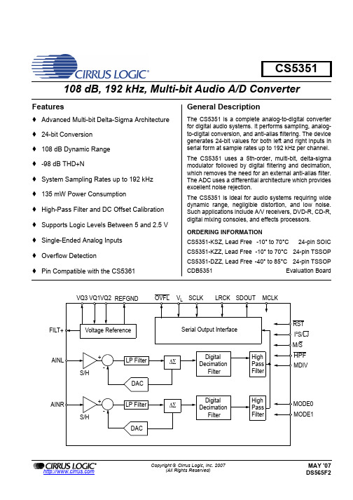
General Description
The CS5351 is a complete analog-to-digital converter for digital audio systems. It performs sampling, analogto-digital conversion, and anti-alias filtering. The device generates 24-bit values for both left and right inputs in serial form at sample rates up to 192 kHz per channel.
4.1 Operational Mode/Sample Rate Range Select .............................................................................. 16 4.2 System Clocking ............................................................................................................................ 16
- 1、下载文档前请自行甄别文档内容的完整性,平台不提供额外的编辑、内容补充、找答案等附加服务。
- 2、"仅部分预览"的文档,不可在线预览部分如存在完整性等问题,可反馈申请退款(可完整预览的文档不适用该条件!)。
- 3、如文档侵犯您的权益,请联系客服反馈,我们会尽快为您处理(人工客服工作时间:9:00-18:30)。
Featuresl Surface Mount Application l 11 thru 200 Volt Voltage Range l Built-in strain relief l Glass passivated junction l Low inductanceMechanical DatalCase: JEDEC DO-214AB Molded plasticover passivated junctionl Terminals solderable per MIL-STD-750, Method 2026 l Standard Packaging: 16mm tape(EIA-481)l Maximum temperature for soldering: 260oC for 10 seconds. l Plastic package has Underwriters LaboratoryFlammability Classification 94V-OMaximum Ratings @ 25o C Unless Otherwise Specified DC Power Dissipation P D 5.0W Pea k forward Surge Curr ent 8.3ms sin gle halfI FS M SeeFig.5 (Note:1 ,2)Operation And Storage Temperature T J , T STG -55o C to +150 o C NOTES:1. Mounted on 8.0mm copper pads to each terminal.2. 8.3ms single half sine-wave, or equivalent square wave,duty cycle = 4 pulses per minute maximum.2omp onents 21201 Itasca Street Chatsworth! "# $ % ! "#(Note: 1 )ELECTRICAL CHARACTERISTICS (T A =25¢J unless otherwise noted, V F =1.2 Max @ I F =1A for all types.Maximum Zener ImpedanceMax reverse Leakage Current@ V RVoltsType No.(Note 1.)Nominal Zener Voltage Vz @ I ZT volts (Note 2.)T est current I ZT mAZ ZT @ I ZT Ohms (Note 2.)Z Zk @ I ZK = 1mA Ohms (Note 2.)I R£g ANon & ASuffixB-Suffix Max Surge Current Ir Amps (Note 3.)Max Voltage Regulation £G Vz, Volts(Note 4.)MaximumRegulator Current I ZM mA (Note 5.)Device Marking Code11121314125100100100 2.52.52.52.512512510075521188.69.410.18.49.19.910.687.576.70.250.250.250.25430395365340348B 349B 350B 351B 15161718197575706565 2.52.52.52.537575757575110.50.50.510.811.512.21313.711.512.212.913.714.4 6.365.85.55.30.250.30.350.40.4315295280265250352B 353B 354B 355B 356B 2022242527655050505033.53.54575751001101200.50.50.50.50.514.415.817.31819.415.216.718.21920.6 5.14.74.44.34.10.40.450.550.550.6237216198190176357B 358B 359B 360B 361B 28303336395040403030681011141301401501601700.50.50.50.50.520.121.623.825.928.121.222.825.127.429.7 3.93.73.53.33.10.60.60.60.650.65170158144132122362B 363B 364B 365B 366B 4347515660302525202020252735401902102302803500.50.50.50.50.53133.836.740.34332.735.838.842.645.5 2.82.72.52.32.20.70.80.911.2110100938679367B 368B 369B 370B 371B 6268758287202020151542444565754005006207207600.50.50.50.50.544.64954596347.151.75662.266 2.121.91.81.7 1.351.51.61.827670635854.5372B 373B 374B 375B 376B 91100110120130151212101075901251701907608001000115012500.50.50.50.50.565.57279.286.493.669.27683.691.298.8 1.61.51.41.31.2 2.22.52.52.52.552.547.54339.536.6377B 378B 379B 380B 381B 1401501601701801908888552303303503804304501500150016501750175018500.50.50.50.50.50.5101108115122130137106114122129137144 1.21.11.1110.9 2.5333453431.629.42826.425382B 383B 384B 385B 386B 387B 200548018500.51441520.9523.6388BNOTE:1. TOLERANCE AND VOLTAGE DESIGNATION - The JEDEC type numbers shown indicate a tolerance of ¡Ó10% with guaranteed limits on only Vz, I R , I r , and V F as shown in the electrical characteristics table. Units with guaranteed limits on all seven parameters are indicated by suffix “B” for ¡Ó5% tolerance.2. ZENER VOLTAGE (Vz) AND IMPEDANCE (Z ZT & Z ZK ) - T est conditions for Zener voltage and impedance are as follows; Iz is applied 40¡Ó10 ms prior to reading. Mounting contacts are located from the inside edge of mounting clips to the body of the diode.(T A =25¢J ¡Ï¢·¡Ð¢±¢J ).SMCJ5348SMCJ5351SMCJ5350SMCJ5349SMCJ5352SMCJ5355SMCJ5354SMCJ5353SMCJ5356SMCJ5357SMCJ5360SMCJ5359SMCJ5358SMCJ5361SMCJ5362SMCJ5365SMCJ5364SMCJ5363SMCJ5366SMCJ5367SMCJ5370SMCJ5369SMCJ5368SMCJ5371SMCJ5372SMCJ5375SMCJ5374SMCJ5373SMCJ5376SMCJ5377SMCJ5380SMCJ5379SMCJ5378SMCJ5381SMCJ5382SMCJ5385SMCJ5384SMCJ5383SMCJ5386SMCJ5387SMCJ53883. SURGE CURRENT (Ir) - Surge current is specified as the maximum allowable peak, non-recurrent square-wavecurrent with a pulse width, PW, of 8.3 ms. The data given in Figure 5 may be used to find the maximum surge current for a quare wave of any pulse width between 1 ms and 1000ms by plotting the applicable points onlogarithmic paper. Examples of this, using the 6.8v and 200V zeners, are shown in Figure 6. Mountingcontact located as specified in Note 3. (T A=25¢J¡Ï¢·¡Ð¢±¢J).4. VOLTAGE REGULATION (£G Vz) - Test conditions for voltage regulation are as follows: Vz measurements are madeat 10% and then at 50% of the Iz max value listed in the electrical characteristics table. The test currents are the same for the 5% and 10% tolerance devices. The test current time druation for each Vz measurement is 40¡Ó10 ms.(T A=25¢J¡Ï¢·¡Ð¢±¢J). Mounting contact located as specified in Note2.5. MAXIMUM REGULATOR CURRENT (I ZM) - The maximum current shown is based on the maximum voltage of a5% type unit. Therefore, it applies only to the B-suffix device. The actual I ZM for any device may not exceed the value of 5 watts divided by the actual Vz of the device. T L=75¢J at maximum from the device body.APPLICATION NOTE:Since the actual voltage available from a given zener diode is temperature dependent, it is necessary to determine junction temperature under any set of operating conditions in order to calculate its value. The following procedure is recommended:Lead Temperature, T L, should be determined from:T L = £c LA P D + T A£c LA is the lead-to-ambient thermal resistance (¢J/W) and P D is the power dissipation.Junction Temperature, T J , may be found from:T J = T L + £G T JL£G T JL is the increase in junction temperature above the lead temperature and may be found from Figure 3 for a train of power pulses or from Figure 4 for dc power.£G T JL = £c JL P DFor worst-case design, using expected limits of Iz, limits of P D and the extremes of T J(£G T J) may be estimated. Changes in voltage, Vz, can then be found from:£G V= £c VZ£G T J£c VZ, the zener voltage temperature coefficient, is fount from Figures 2.Under high power-pulse operation, the zener voltage will vary with time and may also be affected significantly be the zener resistance. For best regulation, keep current excursions as low as possible.Data of Figure 3 should not be used to compute surge capability. Surge limitations are given in Figure 5. They are lower than would be expected by considering only junction temperature, as current crowding effects cause temperatures to be extremely high in small spots resulting in device degradation should the limits of Figure. 5 be exceeded.RATING AND CHARACTERISTICS CURVESTEMPERATURE COEFFICIENTSTL, LEAD TEMPERATURE (¢J )VZ, ZENER VOLTAGE @IZT (VOLTS)Fig. 1-POWER TEMPERATURE DERATING CURVEFig. 2-TEMPERATURE COEFFICIENT-RANGE FOR UNITS6 TO 220 VOLTSTIME (SECONDS)Fig. 3-TYPICAL THERMAL RESPONSEL, LEAD LENGTH TO HEAT SINK (INCH)NOMINAL VZ(V)Fig. 4-TYPICAL THERMAL RESISTANCEFig. 5-MAXIMUM NON-REPETITIVE SURGECURRENT VERSUS NOMINAL ZENERVOLTAGE (SEE NOTE 3)SM C J5348 thru SM C J5388RATING AND CHARACTERISTICS CURVESZENER VOLTAGE VERSUS ZENER CURRENT(FIGURES 7,8, AND 9)110100100010001001010.112345678910VZ, ZENER VOLTAGE (VOLTS)Fig. 6-PEAK SURGE CURRENT VERSUS PULSEWIDTH(SEE NOTE 3)Fig. 7-ZENER VOLTAGE VERSUS ZENER CURRENTVZ = 6.8 THRU 10 VOLTS0.150 6080VZ, ZENER VOLTAGE (VOLTS)0.1VZ, ZENER VOLTAGE (VOLTS)Fig. 8-ZENER VOLTAGE VERSUS ZENER CURRENTVZ = 11 THRU 75 VOLTS Fig. 9-ZENER VOLTAGE VERSUS ZENER CURRENTVZ = 82 THRU 200 VOLTS*** Data of Figure 3 should not be used to compute surge capability. Surge limitations are given in Figure 5. They arelower than would be expected by considering only junction temperature, as current crowding effects causetemperatures to be extremely high in small spots resulting in device degradation should the limits of Figure. 5 be exceededSM C J5348 thru SM C J5388。