SN74F241中文资料
关于74HC244芯片的中文资料

电源电压Vcc 54 4.5 5 5.5 V
74 4.75 5 5.25
输入高电平电ViH 2 V
输入低电平电ViL 54 0.7 V
74 0.8
输出高电平电流IOH 54 -12 mA
74 -15
输出低电平电流IOL 54 12 mA
74 24
求关于74HC244线接收器(3S,两组控制)
简要说明:
244为三态输出的八组缓冲器和总线驱动器,其主要电器特性的典型值如下(不同厂家具体值有差别):
型号 tPLH tphl PD
54LS241/74LS241 12ns 12ns 110mW
引出端符号:
1A1~1A4,2A1~2A4 输入端
/1G, /2G 三态允许端(低电平有效)
1Y1~1Y4,2Y1~2Y4 输出端
逻辑图:
双列直插封装
极限值:
电源电压 …………………………………………. 7V
输入电压 …………………………………………. 5.5V
tPHZ输出由高到高阻态禁止时间 Vcc=5V CL=5pF
RL=90 Ω 18 ns
tPLZ输出由低到高阻态禁止时间 25 ns
静态特性(TA为工作环境温度范围)
参 数 测 试 条 件【1】 LS244 单位
最小 最大
VIK输入嵌位电压 Vcc=最小,Iik=-18mA -1.5 V
输出高阻态时高电平电压 …………………………. 5.5V
工作环境温度
54XXX …………………………………. -55~125℃
74XXX …………………………………. 0~70℃
74ac241,74act241 八路缓冲线驱动器具有3-state输出说明书

74AC241, 74ACT241 Octal Buffer/Line Driver with 3-STATE Outputs74AC241, 74ACT241 Octal Buffer/Line Driver with 3-STATE OutputsTruth TableH = HIGH Voltage Level X = ImmaterialL = LOW Voltage LevelZ = High ImpedanceAbsolute Maximum RatingsStresses exceeding the absolute maximum ratings may damage the device. The device may not function or beoperable above the recommended operating conditions and stressing the parts to these levels is not recommended. In addition, extended exposure to stresses above the recommended operating conditions may affect device reliability. The absolute maximum ratings are stress ratings only.Recommended Operating ConditionsThe Recommended Operating Conditions table defines the conditions for actual device operation. Recommended operating conditions are specified to ensure optimal performance to the datasheet specifications. Fairchild does not recommend exceeding them or designing to absolute maximum ratings.Inputs OutputsInputs OutputsOE 1I nPins 12, 14, 16, 18OE 2I nPins 3, 5, 7, 9L L L H L L L H H H H H HXZLXZSymbol ParameterRatingV CC Supply Voltage –0.5V to +7.0VI IKDC Input Diode Current V I = –0.5V V I = V CC + 0.5V–20mA +20mAV I DC Input Voltage –0.5V to V CC + 0.5VI OKDC Output Diode Current V O = –0.5V V O = V CC + 0.5V–20mA +20mAV O DC Output Voltage–0.5V to V CC + 0.5VI O DC Output Source or Sink Current ±50mA I CC or I GND DC V CC or Ground Current per Output Pin±50mAT STG Storage Temperature –65°C to +150°CT JJunction Temperature140°CSymbol ParameterRatingV CCSupply Voltage AC ACT2.0V to 6.0V 4.5V to 5.5V V I Input Voltage 0V to V CC V O Output Voltage 0V to V CCT A Operating Temperature–40°C to +85°C∆ V / ∆ t Minimum Input Edge Rate, AC Devices:V IN from 30% to 70% of V CC , V CC @ 3.3V , 4.5V , 5.5V 125mV/ns ∆ V / ∆ tMinimum Input Edge Rate, ACT Devices: V IN from 0.8V to 2.0V , V CC@ 4.5V , 5.5V125mV/ns74AC241, 74ACT241 Octal Buffer/Line Driver with 3-STATE OutputsDC Electrical Characteristics for ACNotes:1.All outputs loaded; thresholds on input associated with output under test.2.Maximum test duration 2.0ms, one output loaded at a time.3.I IN and I CC @************************************************************** CC .SymbolParameterV CC (V)ConditionsT A = +25°CT A = –40°C to +85°C UnitsTyp.Guaranteed LimitsV IHMinimum HIGH Level Input Voltage3.0V OUT = 0.1V or V CC – 0.1V 1.5 2.12.1V4.5 2.25 3.15 3.155.5 2.75 3.85 3.85V ILMaximum LOW Level Input Voltage3.0V OUT = 0.1V or V CC – 0.1V 1.50.90.9V4.5 2.25 1.35 1.355.5 2.75 1.65 1.65V OHMinimum HIGHLevel Output Voltage3.0I OUT = –50µA2.99 2.9 2.9V 4.5 4.49 4.4 4.45.55.495.4 5.4V IN = V IL or V IH :3.0I OH = –12mA 2.56 2.464.5I OH = –24mA 3.86 3.765.5I OH = –24mA (1) 4.864.76V OLMaximum LOWLevel Output Voltage3.0I OUT = 50µA0.0020.10.1V 4.50.0010.10.15.50.0010.10.1V IN = V IL or V IH :3.0I OL = 12mA 0.360.444.5I OL = 24mA 0.360.445.5I OL = 24mA (1) 0.360.44I IN (3) Maximum Input Leakage Current 5.5V I = V CC , GND ±0.1±0.1µA IOZMaximum 3-STATE Leakage Current 5.5V I (OE) = V IL , V IH ; V I = V CC , GND; V O = V CC , GND ±0.25±2.5µA I OLD Minimum Dynamic Output Current (2) 5.5V OLD = 1.65V Max.75mA I OHD V OHD = 3.85V Min.–75mA I CC (3)Maximum Quiescent Supply Current5.5V IN = V CC or GND4.040.0µANotes:4.All outputs loaded; thresholds on input associated with output under test.5.Maximum test duration 2.0ms, one output loaded at a time.I CCMaximumQuiescent Supply Current5.5V IN = V CC or GND4.040.0µANote:7.Voltage range 5.0 is 5.0V ± 0.5V.CapacitanceData to Output t PHL Propagation Delay, Data to Output 5.0 1.57.09.0 1.510.0ns t PZH Output Enable Time 5.0 1.5 6.09.0 1.010.0ns t PZL Output Enable Time 5.0 1.57.010.0 1.511.0ns t PHZ Output Disable Time 5.0 1.58.010.5 1.511.5ns t PLZOutput Disable Time5.02.07.010.51.511.5nsSymbolParameterConditionsTyp.UnitsC IN Input CapacitanceV CC = OPEN 4.5pF C PDPower Dissipation CapacitanceV CC = 5.0V45.0pFPackage Number M20B74AC241, 74ACT241 Octal Buffer/Line Driver with 3-STATE Outputs The Power Franchise™TinyBoost。
SN74F163ADRG4,SN74F163ANSR,SN74F163ANSRE4,SN74F163ANSRG4,SN74F163ANE4, 规格书,Datasheet 资料

PACKAGING INFORMATIONOrderable Device Status(1)PackageType PackageDrawingPins PackageQtyEco Plan(2)Lead/Ball Finish MSL Peak Temp(3)SN74F163AD ACTIVE SOIC D1640Green(RoHS&no Sb/Br)CU NIPDAU Level-1-260C-UNLIMSN74F163ADE4ACTIVE SOIC D1640Green(RoHS&no Sb/Br)CU NIPDAU Level-1-260C-UNLIMSN74F163ADG4ACTIVE SOIC D1640Green(RoHS&no Sb/Br)CU NIPDAU Level-1-260C-UNLIMSN74F163ADR ACTIVE SOIC D162500Green(RoHS&no Sb/Br)CU NIPDAU Level-1-260C-UNLIMSN74F163ADRE4ACTIVE SOIC D162500Green(RoHS&no Sb/Br)CU NIPDAU Level-1-260C-UNLIMSN74F163ADRG4ACTIVE SOIC D162500Green(RoHS&no Sb/Br)CU NIPDAU Level-1-260C-UNLIMSN74F163AN ACTIVE PDIP N1625Pb-Free(RoHS)CU NIPDAU N/A for Pkg Type SN74F163AN3OBSOLETE PDIP N16TBD Call TI Call TISN74F163ANE4ACTIVE PDIP N1625Pb-Free(RoHS)CU NIPDAU N/A for Pkg TypeSN74F163ANSR ACTIVE SO NS162000Green(RoHS&no Sb/Br)CU NIPDAU Level-1-260C-UNLIMSN74F163ANSRE4ACTIVE SO NS162000Green(RoHS&no Sb/Br)CU NIPDAU Level-1-260C-UNLIMSN74F163ANSRG4ACTIVE SO NS162000Green(RoHS&no Sb/Br)CU NIPDAU Level-1-260C-UNLIM(1)The marketing status values are defined as follows:ACTIVE:Product device recommended for new designs.LIFEBUY:TI has announced that the device will be discontinued,and a lifetime-buy period is in effect.NRND:Not recommended for new designs.Device is in production to support existing customers,but TI does not recommend using this part in a new design.PREVIEW:Device has been announced but is not in production.Samples may or may not be available.OBSOLETE:TI has discontinued the production of the device.(2)Eco Plan-The planned eco-friendly classification:Pb-Free(RoHS),Pb-Free(RoHS Exempt),or Green(RoHS&no Sb/Br)-please check /productcontent for the latest availability information and additional product content details.TBD:The Pb-Free/Green conversion plan has not been defined.Pb-Free(RoHS):TI's terms"Lead-Free"or"Pb-Free"mean semiconductor products that are compatible with the current RoHS requirements for all6substances,including the requirement that lead not exceed0.1%by weight in homogeneous materials.Where designed to be soldered at high temperatures,TI Pb-Free products are suitable for use in specified lead-free processes.Pb-Free(RoHS Exempt):This component has a RoHS exemption for either1)lead-based flip-chip solder bumps used between the die and package,or2)lead-based die adhesive used between the die and leadframe.The component is otherwise considered Pb-Free(RoHS compatible)as defined above.Green(RoHS&no Sb/Br):TI defines"Green"to mean Pb-Free(RoHS compatible),and free of Bromine(Br)and Antimony(Sb)based flame retardants(Br or Sb do not exceed0.1%by weight in homogeneous material)(3)MSL,Peak Temp.--The Moisture Sensitivity Level rating according to the JEDEC industry standard classifications,and peak solder temperature.Important Information and Disclaimer:The information provided on this page represents TI's knowledge and belief as of the date that it is provided.TI bases its knowledge and belief on information provided by third parties,and makes no representation or warranty as to the accuracy of such information.Efforts are underway to better integrate information from third parties.TI has taken and continues to take reasonable steps to provide representative and accurate information but may not have conducted destructive testing or chemical analysis on incoming materials and chemicals.TI and TI suppliers consider certain information to be proprietary,and thus CAS numbers and other limited information may not be available for release.In no event shall TI's liability arising out of such information exceed the total purchase price of the TI part(s)at issue in this document sold by TI to Customer on an annual basis.TAPE AND REEL INFORMATION*All dimensions are nominalDevicePackage Type Package Drawing Pins SPQReel Diameter (mm)Reel Width W1(mm)A0(mm)B0(mm)K0(mm)P1(mm)W (mm)Pin1Quadrant SN74F163ADR SOIC D 162500330.016.4 6.510.3 2.18.016.0Q1SN74F163ANSRSONS162000330.016.48.210.52.512.016.0Q1*All dimensions are nominalDevice Package Type Package Drawing Pins SPQ Length(mm)Width(mm)Height(mm) SN74F163ADR SOIC D162500333.2345.928.6SN74F163ANSR SO NS162000367.0367.038.0IMPORTANT NOTICETexas Instruments Incorporated and its subsidiaries(TI)reserve the right to make corrections,enhancements,improvements and other changes to its semiconductor products and services per JESD46C and to discontinue any product or service per JESD48B.Buyers should obtain the latest relevant information before placing orders and should verify that such information is current and complete.All semiconductor products(also referred to herein as“components”)are sold subject to TI’s terms and conditions of sale supplied at the time of order acknowledgment.TI warrants performance of its components to the specifications applicable at the time of sale,in accordance with the warranty in TI’s terms and conditions of sale of semiconductor products.Testing and other quality control techniques are used to the extent TI deems necessary to support this warranty.Except where mandated by applicable law,testing of all parameters of each component is not necessarily performed.TI assumes no liability for applications assistance or the design of Buyers’products.Buyers are responsible for their products and applications using TI components.To minimize the risks associated with Buyers’products and applications,Buyers should provide adequate design and operating safeguards.TI does not warrant or represent that any license,either express or implied,is granted under any patent right,copyright,mask work right,or other intellectual property right relating to any combination,machine,or process in which TI components or services are rmation published by TI regarding third-party products or services does not constitute a license to use such products or services or a warranty or endorsement e of such information may require a license from a third party under the patents or other intellectual property of the third party,or a license from TI under the patents or other intellectual property of TI.Reproduction of significant portions of TI information in TI data books or data sheets is permissible only if reproduction is without alteration and is accompanied by all associated warranties,conditions,limitations,and notices.TI is not responsible or liable for such altered rmation of third parties may be subject to additional restrictions.Resale of TI components or services with statements different from or beyond the parameters stated by TI for that component or service voids all express and any implied warranties for the associated TI component or service and is an unfair and deceptive business practice. TI is not responsible or liable for any such statements.Buyer acknowledges and agrees that it is solely responsible for compliance with all legal,regulatory and safety-related requirements concerning its products,and any use of TI components in its applications,notwithstanding any applications-related information or support that may be provided by TI.Buyer represents and agrees that it has all the necessary expertise to create and implement safeguards which anticipate dangerous consequences of failures,monitor failures and their consequences,lessen the likelihood of failures that might cause harm and take appropriate remedial actions.Buyer will fully indemnify TI and its representatives against any damages arising out of the use of any TI components in safety-critical applications.In some cases,TI components may be promoted specifically to facilitate safety-related applications.With such components,TI’s goal is to help enable customers to design and create their own end-product solutions that meet applicable functional safety standards and requirements.Nonetheless,such components are subject to these terms.No TI components are authorized for use in FDA Class III(or similar life-critical medical equipment)unless authorized officers of the parties have executed a special agreement specifically governing such use.Only those TI components which TI has specifically designated as military grade or“enhanced plastic”are designed and intended for use in military/aerospace applications or environments.Buyer acknowledges and agrees that any military or aerospace use of TI components which have not been so designated is solely at the Buyer's risk,and that Buyer is solely responsible for compliance with all legal and regulatory requirements in connection with such use.TI has specifically designated certain components which meet ISO/TS16949requirements,mainly for automotive ponents which have not been so designated are neither designed nor intended for automotive use;and TI will not be responsible for any failure of such components to meet such requirements.Products ApplicationsAudio /audio Automotive and Transportation /automotiveAmplifiers Communications and Telecom /communicationsData Converters Computers and Peripherals /computersDLP®Products Consumer Electronics /consumer-appsDSP Energy and Lighting /energyClocks and Timers /clocks Industrial /industrialInterface Medical /medicalLogic Security /securityPower Mgmt Space,Avionics and Defense /space-avionics-defense Microcontrollers Video and Imaging /videoRFID OMAP Mobile Processors /omap TI E2E Community Wireless Connectivity /wirelessconnectivityMailing Address:Texas Instruments,Post Office Box655303,Dallas,Texas75265Copyright©2012,Texas Instruments Incorporated。
HD74AC241FP中文资料

HD74AC241/HD74ACT241Octal Buffer/Line Driver with 3-State OutputADE-205-382 (Z)1st. EditionSep. 2000 DescriptionThe HD74AC241/HD74ACT241 is an octal buffer and line driver designed to be employed as a memory address driver, clock driver and bus-oriented transmitter or receiver which provides improved PC board density.Features• 3-State Outputs Drive Bus Lines or Buffer Memory Address Registers• Outputs Source/Sink 24 mA• HD74ACT241 has TTL-Compatible InputsPin ArrangementHD74AC241/HD74ACT2412Truth TablesInputs Outputs (Pins 12, 14, 16, 18)OE 1A Y L L L L H H H XZInputs Outputs (Pins 3, 5, 7, 9)OE 2A Y H L L H H H L X ZH :High Voltage Level L :Low Voltage Level X :ImmaterialZ:High ImpedanceDC Characteristics (unless otherwise specified)ItemSymbol Max Unit ConditionMaximum quiescent supply current I CC 80µA V IN = V CC or ground, V CC = 5.5 V,Ta = Worst caseMaximum quiescent supply current I CC 8.0µA V IN = V CC or ground, V CC = 5.5 V,Ta = 25°CMaximum additional I CC /input (HD74ACT241)I CCT1.5mAV IN = V CC – 2.1 V, V CC = 5.5 V,Ta = Worst caseHD74AC241/HD74ACT2413AC Characteristics: HD74AC241Ta = +25°C C L = 50 pFTa = –40°C to +85°C C L = 50 pF ItemSymbol V CC (V)*1Min Typ Max Min Max Unit Propagation delay t PLH3.3 1.0 6.09.0 1.010.0nsData to output 5.0 1.0 5.07.0 1.07.5Propagation delay t PHL 3.3 1.0 6.09.0 1.010.5ns Data to output 5.0 1.0 4.57.0 1.07.5Output enable time t ZH 3.3 1.0 6.512.5 1.013.0ns 5.0 1.0 5.59.0 1.09.5Output enable time t ZL 3.3 1.07.012.0 1.013.0ns 5.0 1.0 5.59.0 1.09.5Output disable time t HZ 3.3 1.08.012.0 1.012.5ns 5.0 1.0 6.510.0 1.010.5Output disable time t LZ 3.3 1.07.012.5 1.013.5ns 5.01.06.010.01.010.5Note:1.Voltage Range 3.3 is 3.3 V ± 0.3 VVoltage Range 5.0 is 5.0 V ± 0.5 VAC Characteristics: HD74ACT241Ta = +25°C C L = 50 pFTa = –40°C to +85°C C L = 50 pF ItemSymbol V CC (V)*1Min Typ Max Min Max Unit Propagation delay Data to output t PLH 5.0 1.0 6.59.0 1.010.0ns Propagation delay Data to output t PHL 5.0 1.07.09.0 1.010.0ns Output enable time t ZH 5.0 1.0 6.09.0 1.010.0ns Output enable time t ZL 5.0 1.07.010.0 1.011.0ns Output disable time t HZ 5.0 1.08.010.5 1.011.5ns Output disable time t LZ5.01.07.010.51.011.5nsNote:1.Voltage Range 5.0 is 5.0 V ± 0.5 VHD74AC241/HD74ACT2414CapacitanceItemSymbol Typ Unit Condition Input capacitanceC IN 4.5pF V CC = 5.5 V Power dissipation capacitanceC PD45.0pFV CC = 5.0 VHD74AC241/HD74ACT241 Package Dimensions5HD74AC241/HD74ACT2416HD74AC241/HD74ACT2417Cautions1.Hitachi neither warrants nor grants licenses of any rights of Hitachi’s or any third party’s patent,copyright, trademark, or other intellectual property rights for information contained in this document.Hitachi bears no responsibility for problems that may arise with third party’s rights, includingintellectual property rights, in connection with use of the information contained in this document.2.Products and product specifications may be subject to change without notice. Confirm that you have received the latest product standards or specifications before final design, purchase or use.3.Hitachi makes every attempt to ensure that its products are of high quality and reliability. However,contact Hitachi’s sales office before using the product in an application that demands especially high quality and reliability or where its failure or malfunction may directly threaten human life or cause risk of bodily injury, such as aerospace, aeronautics, nuclear power, combustion control, transportation,traffic, safety equipment or medical equipment for life support.4.Design your application so that the product is used within the ranges guaranteed by Hitachi particularly for maximum rating, operating supply voltage range, heat radiation characteristics, installationconditions and other characteristics. Hitachi bears no responsibility for failure or damage when used beyond the guaranteed ranges. Even within the guaranteed ranges, consider normally foreseeable failure rates or failure modes in semiconductor devices and employ systemic measures such as fail-safes, so that the equipment incorporating Hitachi product does not cause bodily injury, fire or other consequential damage due to operation of the Hitachi product.5.This product is not designed to be radiation resistant.6.No one is permitted to reproduce or duplicate, in any form, the whole or part of this document without written approval from Hitachi.7.Contact Hitachi’s sales office for any questions regarding this document or Hitachi semiconductor products.Hitachi, Ltd.Semiconductor & Integrated Circuits.Nippon Bldg., 2-6-2, Ohte-machi, Chiyoda-ku, Tokyo 100-0004, Japan Tel: Tokyo (03) 3270-2111 Fax: (03) 3270-5109Copyright © Hitachi, Ltd., 2000. All rights reserved. Printed in Japan.Hitachi Asia Ltd. Hitachi Tower16 Collyer Quay #20-00, Singapore 049318Tel : <65>-538-6533/538-8577 Fax : <65>-538-6933/538-3877URL : .sg URLNorthAmerica : /Europe : /hel/ecg Asia : Japan : http://www.hitachi.co.jp/Sicd/indx.htmHitachi Asia Ltd.(Taipei Branch Office)4/F, No. 167, Tun Hwa North Road, Hung-Kuo Building, Taipei (105), Taiwan Tel : <886>-(2)-2718-3666 Fax : <886>-(2)-2718-8180 Telex : 23222 HAS-TPURL : Hitachi Asia (Hong Kong) Ltd. Group III (Electronic Components) 7/F., North Tower, World Finance Centre,Harbour City, Canton Road Tsim Sha Tsui, Kowloon, Hong KongTel : <852>-(2)-735-9218 Fax : <852>-(2)-730-0281URL : Hitachi Europe Ltd.Electronic Components Group.Whitebrook ParkLower Cookham Road MaidenheadBerkshire SL6 8YA, United Kingdom Tel: <44> (1628) 585000Fax: <44> (1628) 585160Hitachi Europe GmbHElectronic Components Group Dornacher Stra βe 3D-85622 Feldkirchen, Munich GermanyTel: <49> (89) 9 9180-0Fax: <49> (89) 9 29 30 00Hitachi Semiconductor (America) Inc.179 East Tasman Drive,San Jose,CA 95134 Tel: <1> (408) 433-1990Fax: <1>(408) 433-0223For further information write to:Colophon 2.0。
集成电路IC芯片中文名称大全
专业 诚信 合作共赢!
010-57194553 13911315253
北京京华特科技有限公司 -------- 专业元器件供应商
SN7407 六缓冲器/驱动器
SN74HC03
SN7414 六缓冲器/驱动器
SN74HC04
SN7416 六反相缓冲器/驱动器 SN74HC05
SN74LS126
SN74LS133 13 输入与非门
SN74LS132
SN74LS137 地址锁存 3-8 线译码器 SN74LS136
SN74LS139 双 2-4 线译码-转换器 SN74LS138
SN74LS147 10-4 线优先编码器 SN74LS145
SN74LS153 双 4 选 1 数据选择器 SN74LS148
专业 诚信 合作共赢!
010-57194553 13911315253
北京京华特科技有限公司 -------- 专业元器件供应商
SN74LS92 12 分频计数器
SN74LS93
SN74LS96 5 位移位寄存器
SN74LS95
SN74LS273
SN74LS283 4 位二进制全加器
SN74LS276
SN74LS293 4 位二进制计数器
SN74LS280
SN74LS365 六缓冲器带公用启动器 SN74LS290
SN74LS367 六总线三态输出缓冲器 SN74LS295
SN74LS373 8D 锁存器 SN74LS375 4 位双稳锁存器 SN74LS386 四 2 输入异或门 SN74LS393 双 4 位二进制计数器 SN74LS574 8 位 D 型触发器
SN74LS155 双 2-4 线多路分配器 SN74LS151
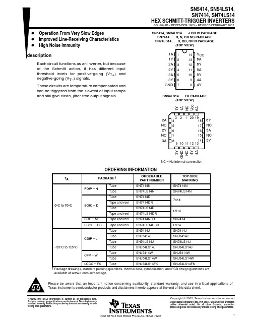
SN74LS14N3中文资料
InputV T OutputPACKAGING INFORMATIONOrderable Device Status(1)PackageType PackageDrawingPins PackageQtyEco Plan(2)Lead/Ball Finish MSL Peak Temp(3)5962-9665801Q2A ACTIVE LCCC FK201TBD Call TI Level-NC-NC-NC 5962-9665801QCA ACTIVE CDIP J141TBD Call TI Level-NC-NC-NC 5962-9665801QDA ACTIVE CFP W141TBD Call TI Level-NC-NC-NC 5962-9665801VCA ACTIVE CDIP J141TBD Call TI Level-NC-NC-NC 5962-9665801VDA ACTIVE CFP W141TBD Call TI Level-NC-NC-NC JM38510/31302BCA ACTIVE CDIP J141TBD Call TI Level-NC-NC-NC SN5414J ACTIVE CDIP J141TBD Call TI Level-NC-NC-NC SN54LS14J ACTIVE CDIP J141TBD Call TI Level-NC-NC-NCSN7414D ACTIVE SOIC D1450Pb-Free(RoHS)CU NIPDAU Level-2-260C-1YEAR/Level-1-235C-UNLIMSN7414DE4ACTIVE SOIC D1450Pb-Free(RoHS)CU NIPDAU Level-2-260C-1YEAR/Level-1-235C-UNLIMSN7414DR ACTIVE SOIC D142500Pb-Free(RoHS)CU NIPDAU Level-2-260C-1YEAR/Level-1-235C-UNLIMSN7414DRE4ACTIVE SOIC D142500Pb-Free(RoHS)CU NIPDAU Level-2-260C-1YEAR/Level-1-235C-UNLIMSN7414N ACTIVE PDIP N1425Pb-Free(RoHS)CU NIPDAU Level-NC-NC-NC SN7414N3OBSOLETE PDIP N14TBD Call TI Call TISN7414NSR ACTIVE SO NS142000Pb-Free(RoHS)CU NIPDAU Level-2-260C-1YEAR/Level-1-235C-UNLIMSN7414NSRE4ACTIVE SO NS142000Pb-Free(RoHS)CU NIPDAU Level-2-260C-1YEAR/Level-1-235C-UNLIMSN74LS14D ACTIVE SOIC D1450Pb-Free(RoHS)CU NIPDAU Level-2-260C-1YEAR/Level-1-235C-UNLIMSN74LS14DBR ACTIVE SSOP DB142000Pb-Free(RoHS)CU NIPDAU Level-2-260C-1YEAR/Level-1-235C-UNLIMSN74LS14DBRE4ACTIVE SSOP DB142000Pb-Free(RoHS)CU NIPDAU Level-2-260C-1YEAR/Level-1-235C-UNLIMSN74LS14DR ACTIVE SOIC D142500Pb-Free(RoHS)CU NIPDAU Level-2-260C-1YEAR/Level-1-235C-UNLIMSN74LS14N ACTIVE PDIP N1425Pb-Free(RoHS)CU NIPDAU Level-NC-NC-NC SN74LS14N3OBSOLETE PDIP N14TBD Call TI Call TISN74LS14NE4ACTIVE PDIP N1425TBD Call TI Call TISN74LS14NSRG4ACTIVE SO NS142000Green(RoHS&no Sb/Br)CU NIPDAU Level-1-260C-UNLIM SNJ5414J ACTIVE CDIP J141TBD Call TI Level-NC-NC-NCSNJ5414W ACTIVE CFP W141TBD Call TI Level-NC-NC-NC SNJ54LS14FK ACTIVE LCCC FK201TBD Call TI Level-NC-NC-NC SNJ54LS14J ACTIVE CDIP J141TBD Call TI Level-NC-NC-NC SNJ54LS14W ACTIVE CFP W141TBD Call TI Level-NC-NC-NC (1)The marketing status values are defined as follows:ACTIVE:Product device recommended for new designs.LIFEBUY:TI has announced that the device will be discontinued,and a lifetime-buy period is in effect.NRND:Not recommended for new designs.Device is in production to support existing customers,but TI does not recommend using this part in a new design.PREVIEW:Device has been announced but is not in production.Samples may or may not be available.OBSOLETE:TI has discontinued the production of the device.(2)Eco Plan-The planned eco-friendly classification:Pb-Free(RoHS)or Green(RoHS&no Sb/Br)-please check /productcontent for the latest availability information and additional product content details.TBD:The Pb-Free/Green conversion plan has not been defined.Pb-Free(RoHS):TI's terms"Lead-Free"or"Pb-Free"mean semiconductor products that are compatible with the current RoHS requirements for all6substances,including the requirement that lead not exceed0.1%by weight in homogeneous materials.Where designed to be soldered at high temperatures,TI Pb-Free products are suitable for use in specified lead-free processes.Green(RoHS&no Sb/Br):TI defines"Green"to mean Pb-Free(RoHS compatible),and free of Bromine(Br)and Antimony(Sb)based flame retardants(Br or Sb do not exceed0.1%by weight in homogeneous material)(3)MSL,Peak Temp.--The Moisture Sensitivity Level rating according to the JEDEC industry standard classifications,and peak solder temperature.Important Information and Disclaimer:The information provided on this page represents TI's knowledge and belief as of the date that it is provided.TI bases its knowledge and belief on information provided by third parties,and makes no representation or warranty as to the accuracy of such information.Efforts are underway to better integrate information from third parties.TI has taken and continues to take reasonable steps to provide representative and accurate information but may not have conducted destructive testing or chemical analysis on incoming materials and chemicals.TI and TI suppliers consider certain information to be proprietary,and thus CAS numbers and other limited information may not be available for release.In no event shall TI's liability arising out of such information exceed the total purchase price of the TI part(s)at issue in this document sold by TI to Customer on an annual basis.元器件交易网IMPORTANT NOTICETexas Instruments Incorporated and its subsidiaries (TI) reserve the right to make corrections, modifications,enhancements, improvements, and other changes to its products and services at any time and to discontinueany product or service without notice. Customers should obtain the latest relevant information before placingorders and should verify that such information is current and complete. All products are sold subject to TI’s termsand conditions of sale supplied at the time of order acknowledgment.TI warrants performance of its hardware products to the specifications applicable at the time of sale inaccordance with TI’s standard warranty. T esting and other quality control techniques are used to the extent TIdeems necessary to support this warranty. Except where mandated by government requirements, testing of allparameters of each product is not necessarily performed.TI assumes no liability for applications assistance or customer product design. Customers are responsible fortheir products and applications using TI components. T o minimize the risks associated with customer productsand applications, customers should provide adequate design and operating safeguards.TI does not warrant or represent that any license, either express or implied, is granted under any TI patent right,copyright, mask work right, or other TI intellectual property right relating to any combination, machine, or processin which TI products or services are used. Information published by TI regarding third-party products or servicesdoes not constitute a license from TI to use such products or services or a warranty or endorsement thereof.Use of such information may require a license from a third party under the patents or other intellectual propertyof the third party, or a license from TI under the patents or other intellectual property of TI.Reproduction of information in TI data books or data sheets is permissible only if reproduction is withoutalteration and is accompanied by all associated warranties, conditions, limitations, and notices. Reproductionof this information with alteration is an unfair and deceptive business practice. TI is not responsible or liable forsuch altered documentation.Resale of TI products or services with statements different from or beyond the parameters stated by TI for thatproduct or service voids all express and any implied warranties for the associated TI product or service andis an unfair and deceptive business practice. TI is not responsible or liable for any such statements.Following are URLs where you can obtain information on other Texas Instruments products and applicationsolutions:Products ApplicationsAmplifiers Audio /audioData Converters Automotive /automotiveDSP Broadband /broadbandInterface Digital Control /digitalcontrolLogic Military /militaryPower Mgmt Optical Networking /opticalnetworkMicrocontrollers Security /securityTelephony /telephonyVideo & Imaging /videoWireless /wirelessMailing Address:Texas InstrumentsPost Office Box 655303 Dallas, Texas 75265Copyright 2005, Texas Instruments Incorporated。
SN74AC245PWLE中文资料

PACKAGING INFORMATIONOrderable Device Status(1)PackageType PackageDrawingPins PackageQtyEco Plan(2)Lead/Ball Finish MSL Peak Temp(3)5962-87758012A ACTIVE LCCC FK201TBD POST-PLATE N/A for Pkg Type 5962-8775801RA ACTIVE CDIP J201TBD A42SNPB N/A for Pkg Type 5962-8775801SA ACTIVE CFP W201TBD A42N/A for Pkg Type 5962-8775801VRA ACTIVE CDIP J201TBD A42SNPB N/A for Pkg Type5962-8775801VSA ACTIVE CFP W201TBD A42N/A for Pkg Type SN74AC245DBLE OBSOLETE SSOP DB20TBD Call TI Call TISN74AC245DBR ACTIVE SSOP DB202000Green(RoHS&no Sb/Br)CU NIPDAU Level-1-260C-UNLIMSN74AC245DBRE4ACTIVE SSOP DB202000Green(RoHS&no Sb/Br)CU NIPDAU Level-1-260C-UNLIMSN74AC245DW ACTIVE SOIC DW2025Green(RoHS&no Sb/Br)CU NIPDAU Level-1-260C-UNLIMSN74AC245DWE4ACTIVE SOIC DW2025Green(RoHS&no Sb/Br)CU NIPDAU Level-1-260C-UNLIMSN74AC245DWR ACTIVE SOIC DW202000Green(RoHS&no Sb/Br)CU NIPDAU Level-1-260C-UNLIMSN74AC245DWRE4ACTIVE SOIC DW202000Green(RoHS&no Sb/Br)CU NIPDAU Level-1-260C-UNLIMSN74AC245N ACTIVE PDIP N2020Pb-Free(RoHS)CU NIPDAU N/A for Pkg TypeSN74AC245NE4ACTIVE PDIP N2020Pb-Free(RoHS)CU NIPDAU N/A for Pkg TypeSN74AC245NSR ACTIVE SO NS202000Green(RoHS&no Sb/Br)CU NIPDAU Level-1-260C-UNLIMSN74AC245NSRE4ACTIVE SO NS202000Green(RoHS&no Sb/Br)CU NIPDAU Level-1-260C-UNLIMSN74AC245PW ACTIVE TSSOP PW2070Green(RoHS&no Sb/Br)CU NIPDAU Level-1-260C-UNLIMSN74AC245PWE4ACTIVE TSSOP PW2070Green(RoHS&no Sb/Br)CU NIPDAU Level-1-260C-UNLIM SN74AC245PWLE OBSOLETE TSSOP PW20TBD Call TI Call TISN74AC245PWR ACTIVE TSSOP PW202000Green(RoHS&no Sb/Br)CU NIPDAU Level-1-260C-UNLIMSN74AC245PWRE4ACTIVE TSSOP PW202000Green(RoHS&no Sb/Br)CU NIPDAU Level-1-260C-UNLIM SNJ54AC245FK ACTIVE LCCC FK201TBD POST-PLATE N/A for Pkg Type SNJ54AC245J ACTIVE CDIP J201TBD A42SNPB N/A for Pkg Type SNJ54AC245W ACTIVE CFP W201TBD A42N/A for Pkg Type (1)The marketing status values are defined as follows:ACTIVE:Product device recommended for new designs.LIFEBUY:TI has announced that the device will be discontinued,and a lifetime-buy period is in effect.NRND:Not recommended for new designs.Device is in production to support existing customers,but TI does not recommend using this part in a new design.PREVIEW:Device has been announced but is not in production.Samples may or may not be available.OBSOLETE:TI has discontinued the production of the device.(2)Eco Plan-The planned eco-friendly classification:Pb-Free(RoHS),Pb-Free(RoHS Exempt),or Green(RoHS&no Sb/Br)-please check /productcontent for the latest availability information and additional product content details.6-Dec-2006TBD:The Pb-Free/Green conversion plan has not been defined.Pb-Free (RoHS):TI's terms "Lead-Free"or "Pb-Free"mean semiconductor products that are compatible with the current RoHS requirements for all 6substances,including the requirement that lead not exceed 0.1%by weight in homogeneous materials.Where designed to be soldered at high temperatures,TI Pb-Free products are suitable for use in specified lead-free processes.Pb-Free (RoHS Exempt):This component has a RoHS exemption for either 1)lead-based flip-chip solder bumps used between the die and package,or 2)lead-based die adhesive used between the die and leadframe.The component is otherwise considered Pb-Free (RoHS compatible)as defined above.Green (RoHS &no Sb/Br):TI defines "Green"to mean Pb-Free (RoHS compatible),and free of Bromine (Br)and Antimony (Sb)based flame retardants (Br or Sb do not exceed 0.1%by weight in homogeneous material)(3)MSL,Peak Temp.--The Moisture Sensitivity Level rating according to the JEDEC industry standard classifications,and peak solder temperature.Important Information and Disclaimer:The information provided on this page represents TI's knowledge and belief as of the date that it is provided.TI bases its knowledge and belief on information provided by third parties,and makes no representation or warranty as to the accuracy of such information.Efforts are underway to better integrate information from third parties.TI has taken and continues to take reasonable steps to provide representative and accurate information but may not have conducted destructive testing or chemical analysis on incoming materials and chemicals.TI and TI suppliers consider certain information to be proprietary,and thus CAS numbers and other limited information may not be available for release.In no event shall TI's liability arising out of such information exceed the total purchase price of the TI part(s)at issue in this document sold by TI to Customer on an annualbasis.6-Dec-2006TAPE AND REELINFORMATION24-Apr-2007DevicePackage Pins SiteReel Diameter (mm)Reel Width (mm)A0(mm)B0(mm)K0(mm)P1(mm)W (mm)Pin1Quadrant SN74AC245DBR DB 20MLA 330168.27.5 2.51216Q1SN74AC245DWR DW 20MLA 3302410.813.0 2.71224Q1SN74AC245NSRNS 20MLA 330248.213.0 2.51224Q1SN74AC245PWRPW20MLA330166.957.11.6816Q1TAPE AND REEL BOX INFORMATIONDevice Package Pins Site Length (mm)Width (mm)Height (mm)SN74AC245DBR DB 20MLA 333.2333.228.58SN74AC245DWR DW 20MLA 333.2333.231.75SN74AC245NSR NS 20MLA 333.2333.231.75SN74AC245PWRPW20MLA333.2333.228.5824-Apr-200724-Apr-2007IMPORTANT NOTICETexas Instruments Incorporated and its subsidiaries(TI)reserve the right to make corrections,modifications,enhancements, improvements,and other changes to its products and services at any time and to discontinue any product or service without notice. Customers should obtain the latest relevant information before placing orders and should verify that such information is current and complete.All products are sold subject to TI’s terms and conditions of sale supplied at the time of order acknowledgment.TI warrants performance of its hardware products to the specifications applicable at the time of sale in accordance with TI’s standard warranty.Testing and other quality control techniques are used to the extent TI deems necessary to support this warranty.Except where mandated by government requirements,testing of all parameters of each product is not necessarily performed.TI assumes no liability for applications assistance or customer product design.Customers are responsible for their products and applications using TI components.To minimize the risks associated with customer products and applications,customers should provide adequate design and operating safeguards.TI does not warrant or represent that any license,either express or implied,is granted under any TI patent right,copyright,mask work right,or other TI intellectual property right relating to any combination,machine,or process in which TI products or services are rmation published by TI regarding third-party products or services does not constitute a license from TI to use such products or services or a warranty or endorsement e of such information may require a license from a third party under the patents or other intellectual property of the third party,or a license from TI under the patents or other intellectual property of TI. Reproduction of information in TI data books or data sheets is permissible only if reproduction is without alteration and is accompanied by all associated warranties,conditions,limitations,and notices.Reproduction of this information with alteration is an unfair and deceptive business practice.TI is not responsible or liable for such altered documentation.Resale of TI products or services with statements different from or beyond the parameters stated by TI for that product or service voids all express and any implied warranties for the associated TI product or service and is an unfair and deceptive business practice.TI is not responsible or liable for any such statements.TI products are not authorized for use in safety-critical applications(such as life support)where a failure of the TI product would reasonably be expected to cause severe personal injury or death,unless officers of the parties have executed an agreement specifically governing such use.Buyers represent that they have all necessary expertise in the safety and regulatory ramifications of their applications,and acknowledge and agree that they are solely responsible for all legal,regulatory and safety-related requirements concerning their products and any use of TI products in such safety-critical applications,notwithstanding any applications-related information or support that may be provided by TI.Further,Buyers must fully indemnify TI and its representatives against any damages arising out of the use of TI products in such safety-critical applications.TI products are neither designed nor intended for use in military/aerospace applications or environments unless the TI products are specifically designated by TI as military-grade or"enhanced plastic."Only products designated by TI as military-grade meet military specifications.Buyers acknowledge and agree that any such use of TI products which TI has not designated as military-grade is solely at the Buyer's risk,and that they are solely responsible for compliance with all legal and regulatory requirements in connection with such use.TI products are neither designed nor intended for use in automotive applications or environments unless the specific TI products are designated by TI as compliant with ISO/TS16949requirements.Buyers acknowledge and agree that,if they use anynon-designated products in automotive applications,TI will not be responsible for any failure to meet such requirements. Following are URLs where you can obtain information on other Texas Instruments products and application solutions:Products ApplicationsAmplifiers Audio /audioData Converters Automotive /automotiveDSP Broadband /broadbandInterface Digital Control /digitalcontrolLogic Military /militaryPower Mgmt Optical Networking /opticalnetworkMicrocontrollers Security /securityLow Power /lpw Telephony /telephonyWirelessVideo&Imaging /videoWireless /wirelessMailing Address:Texas Instruments,Post Office Box655303,Dallas,Texas75265Copyright©2007,Texas Instruments Incorporated。
SN74BCT2414DW;SN74BCT2414DWR;SN74BCT2414DWRE4;SN74BCT2414DWRG4;SN74BCT2414N;中文规格书,Datasheet资料
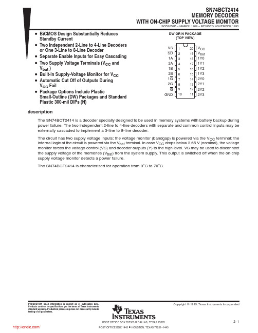
PACKAGING INFORMATIONOrderable Device Status (1)Package Type Package Drawing Pins Package Qty Eco Plan (2)Lead/Ball Finish MSL Peak Temp (3)SN74BCT2414DW ACTIVE SOIC DW 2025Green (RoHS &no Sb/Br)CU NIPDAU Level-1-260C-UNLIM SN74BCT2414DWG4ACTIVE SOIC DW 2025Green (RoHS &no Sb/Br)CU NIPDAU Level-1-260C-UNLIM SN74BCT2414DWR ACTIVE SOIC DW 202000Green (RoHS &no Sb/Br)CU NIPDAU Level-1-260C-UNLIM SN74BCT2414DWRE4ACTIVE SOIC DW 202000Green (RoHS &no Sb/Br)CU NIPDAU Level-1-260C-UNLIM SN74BCT2414DWRG4ACTIVE SOIC DW 202000Green (RoHS &no Sb/Br)CU NIPDAU Level-1-260C-UNLIM SN74BCT2414N ACTIVE PDIP N 2020Pb-Free (RoHS)CU NIPDAU N /A for Pkg Type SN74BCT2414NE4ACTIVEPDIPN2020Pb-Free (RoHS)CU NIPDAUN /A for Pkg Type(1)The marketing status values are defined as follows:ACTIVE:Product device recommended for new designs.LIFEBUY:TI has announced that the device will be discontinued,and a lifetime-buy period is in effect.NRND:Not recommended for new designs.Device is in production to support existing customers,but TI does not recommend using this part in a new design.PREVIEW:Device has been announced but is not in production.Samples may or may not be available.OBSOLETE:TI has discontinued the production of the device.(2)Eco Plan -The planned eco-friendly classification:Pb-Free (RoHS),Pb-Free (RoHS Exempt),or Green (RoHS &no Sb/Br)-please check /productcontent for the latest availability information and additional product content details.TBD:The Pb-Free/Green conversion plan has not been defined.Pb-Free (RoHS):TI's terms "Lead-Free"or "Pb-Free"mean semiconductor products that are compatible with the current RoHS requirements for all 6substances,including the requirement that lead not exceed 0.1%by weight in homogeneous materials.Where designed to be soldered at high temperatures,TI Pb-Free products are suitable for use in specified lead-free processes.Pb-Free (RoHS Exempt):This component has a RoHS exemption for either 1)lead-based flip-chip solder bumps used between the die and package,or 2)lead-based die adhesive used between the die and leadframe.The component is otherwise considered Pb-Free (RoHS compatible)as defined above.Green (RoHS &no Sb/Br):TI defines "Green"to mean Pb-Free (RoHS compatible),and free of Bromine(Br)and Antimony (Sb)based flame retardants (Br or Sb do not exceed 0.1%by weight in homogeneous material)(3)MSL,Peak Temp.--The Moisture Sensitivity Level rating according to the JEDEC industry standard classifications,and peak solder temperature.Important Information and Disclaimer:The information provided on this page represents TI's knowledge and belief as of the date that it is provided.TI bases its knowledge and belief on information provided by third parties,and makes no representation or warranty as to the accuracy of such information.Efforts are underway to better integrate information from third parties.TI has taken and continues to take reasonable steps to provide representative and accurate information but may not have conducted destructive testing or chemical analysis on incoming materials and chemicals.TI and TI suppliers consider certain information to be proprietary,and thus CAS numbers and other limited information may not be available for release.In no event shall TI's liability arising out of such information exceed the total purchase price of the TI part(s)at issue in this document sold by TI to Customer on an annual basis.PACKAGE OPTION ADDENDUM18-Sep-2008TAPE AND REEL INFORMATION*All dimensions are nominalDevicePackage Type Package Drawing Pins SPQReel Diameter (mm)Reel Width W1(mm)A0(mm)B0(mm)K0(mm)P1(mm)W (mm)Pin1Quadrant SN74BCT2414DWR SOICDW202000330.024.410.813.02.712.024.0Q1*All dimensions are nominalDevice Package Type Package Drawing Pins SPQ Length(mm)Width(mm)Height(mm)SN74BCT2414DWR SOIC DW202000367.0367.045.0分销商库存信息:TISN74BCT2414DW SN74BCT2414DWR SN74BCT2414DWRE4 SN74BCT2414DWRG4SN74BCT2414N SN74BCT2414NE4 SN74BCT2414DWG4。
- 1、下载文档前请自行甄别文档内容的完整性,平台不提供额外的编辑、内容补充、找答案等附加服务。
- 2、"仅部分预览"的文档,不可在线预览部分如存在完整性等问题,可反馈申请退款(可完整预览的文档不适用该条件!)。
- 3、如文档侵犯您的权益,请联系客服反馈,我们会尽快为您处理(人工客服工作时间:9:00-18:30)。
元器件交易网
IMPORTANT NOTICE
Texas Instruments and its subsidiaries (TI) reserve the right to make changes to their products or to discontinue
any product or service without notice, and advise customers to obtain the latest version of relevant information
to verify, before placing orders, that information being relied on is current and complete. All products are sold
subject to the terms and conditions of sale supplied at the time of order acknowledgement, including those
pertaining to warranty, patent infringement, and limitation of liability.
TI warrants performance of its semiconductor products to the specifications applicable at the time of sale in
accordance with TI’s standard warranty. Testing and other quality control techniques are utilized to the extent
TI deems necessary to support this warranty. Specific testing of all parameters of each device is not necessarily
performed, except those mandated by government requirements.
CERTAIN APPLICATIONS USING SEMICONDUCTOR PRODUCTS MAY INVOLVE POTENTIAL RISKS OF
DEATH, PERSONAL INJURY, OR SEVERE PROPERTY OR ENVIRONMENTAL DAMAGE (“CRITICAL
APPLICATIONS”). TI SEMICONDUCTOR PRODUCTS ARE NOT DESIGNED, AUTHORIZED, OR
WARRANTED TO BE SUITABLE FOR USE IN LIFE-SUPPORT DEVICES OR SYSTEMS OR OTHER
CRITICAL APPLICATIONS. INCLUSION OF TI PRODUCTS IN SUCH APPLICATIONS IS UNDERSTOOD TO
BE FULLY AT THE CUSTOMER’S RISK.
In order to minimize risks associated with the customer’s applications, adequate design and operating
safeguards must be provided by the customer to minimize inherent or procedural hazards.
TI assumes no liability for applications assistance or customer product design. TI does not warrant or represent
that any license, either express or implied, is granted under any patent right, copyright, mask work right, or other
intellectual property right of TI covering or relating to any combination, machine, or process in which such
semiconductor products or services might be or are used. TI’s publication of information regarding any third
party’s products or services does not constitute TI’s approval, warranty or endorsement thereof.
Copyright © 1998, Texas Instruments Incorporated。