Datasheet_CY8CTMA340_Brief
RCP890A03 datasheet

SpecificationForLTCC 3dB Hybrid Coupler Model Name : RCP890A03RN2 Technologies co., Ltd.RN2 Technologies co., Ltd.284-2, Galgot-ri, Jinwe-myeon, Pyeongtaek-si, Kyunggi-do, KOREA Phone : (+82) 31 - 376 - 5400FAX : (+82) 31 - 376 - 9151 Distributor:Shenzhen Jushou electronics Co., Ltd.6F,building3,Sege science park, futian shenzhen Tel: 0086-0755-******** Mobile:0086-136******** Email: Fisher@Contact:Mr yu1. Description1-1. Part number: RCP890A031-2. Features- Hybrid Coupler 3dB, 90˚- Surface mount type- Suitable for operation frequency 815~960MHz- RoHS compliance- High stability in temperature and humidity for LTCC base - Low loss for Silver(Ag) conductor- Miniature size and high power capability- Lead-free alloy solderable- Thermal expansion corresponding with common substrate 2. Electrical SpecificationFreq. (MHz) Amplitude Balancemax (dB)Isolationmin (dB)Insertion Lossmax (dB)815-960 ±0.15 -23 -0.15VSWR MaxPhase(degrees)Power CapacityAvg. (Watt)Operating Temp.(℃)1.2 90 ±2.0 200 -55 to +1253. Mechanical Specification 3-1. Outline Dimension3-2. Weight- 1.35 Grams typical4. Port ConfigurationConfiguration Port 1 Port 2 Port 3 Port 4Case 1. Input Isolated Coupling-3dB, 0˚Output-3dB, -90˚Case 2. Isolated Input Output-3dB, 90˚Coupling -3dB, 0˚Case 3. Coupling-3dB, 0˚Output-3dB, 90˚Input IsolatedCase 4.Output-3dB, 90˚Coupling-3dB, 0˚Isolated Input * Once Port 1 is determined, the other three ports are defined automatically.5. Schematic DrawingPort1P inP cou P out P isoPort3 Port4Port26. Typical Performance Data (25℃)Return Loss [dB]Freq. [MHz]Coupling[dB]Out [dB] IL [dB]Amp.Bal.[dB]Phase[degree]S11 S22 S33 S44815 -3.12 -3.07 -0.09 ±0.02 -90.22 -26.15 -27.56 -26.33 -25.85 820 -3.11 -3.08 -0.08 ±0.02 -90.19 -26.37 -27.85 -26.56 -26.07 830 -3.11 -3.10 -0.09 ±0.00 -90.21 -26.85 -28.42 -27.07 -26.52 840 -3.09 -3.11 -0.09 ±0.01 -90.27 -27.34 -29.01 -27.61 -26.97 850 -3.09 -3.13 -0.10 ±0.02 -90.36 -27.92 -29.68 -28.18 -27.47 860 -3.08 -3.13 -0.09 ±0.03 -90.31 -28.50 -30.34 -28.82 -27.99 870 -3.07 -3.13 -0.09 ±0.03 -90.36 -29.12 -31.06 -29.44 -28.53 880 -3.06 -3.14 -0.09 ±0.04 -90.39 -29.81 -31.71 -30.12 -29.12 890 -3.07 -3.16 -0.11 ±0.05 -90.38 -30.50 -32.40 -30.84 -29.72 900 -3.06 -3.14 -0.09 ±0.04 -90.39 -31.22 -32.98 -31.48 -30.27 910 -3.06 -3.14 -0.09 ±0.04 -90.43 -31.95 -33.45 -32.22 -30.88 920 -3.06 -3.16 -0.10 ±0.05 -90.46 -32.69 -33.70 -32.94 -31.45 930 -3.06 -3.15 -0.09 ±0.04 -90.54 -33.41 -33.71 -33.55 -31.92 940 -3.07 -3.14 -0.10 ±0.04 -90.48 -34.05 -33.48 -34.03 -32.38 950 -3.07 -3.13 -0.09 ±0.03 -90.51 -34.53 -33.00 -34.41 -32.73 960 -3.08 -3.14 -0.10 ±0.03 -90.55 -34.72 -32.38 -34.50 -32.89* Data with PCB and Connector Loss ( 0.89 GHz = 0.03dB )7. Operation Temperature Curve (a)RCP650A03 Return Loss(Port1)M a g n i t u d e [d B ]Frequency[MHz]RCP890A03 Return Loss(Port2)M a g n i t u d e [d B ]Frequency[MHz]70080090010001100RCP890A03 Return Loss(Port3)M a g n i t u d e [d B ]Frequency[MHz]70080090010001100RCP890A03 Return Loss(Port4)M a g n i t u d e [d B ]Frequency[MHz]8. Operation Temperature Curve (b)70080090010001100RCP890A03 Coupling & Transmission LossM a g n i t u d e [d B ]Frequency[MHz]70080090010001100RCP890A03 Insertion LossM a g n i t u d e [d B ]Frequency[MHz]70080090010001100RCP890A03 IsolationM a g n i t u d e [d B ]Frequency[MHz]70080090010001100RCP890A03 Phase BalanceP h a s e [d e g ]Frequency[MHz]9. Test Method- Refer to ‘Case 1’ of ‘4. Port Configuration’ on page 4 - Have the network analyzer calibrated properly.- Measure the data of Coupling through port 1 to port 3. (S31) - Measure the data of Transmission through port 1 to port 4. (S41) - Measure the data of Isolation through port 1 to port 2. (S21)- Calculate the Insertion Loss and Amplitude Balance of coupler on the below power method formula.in out P cou : Power of Coupling Port P iso : Power of Isolated Port10. Measurement board layout11. Recommended PCB layout and Solder mask pattern12. Reflow profilePeakSoakingUpPre-HeatingRamp℃ T1:160±5℃ T2:180±5℃ T4:260±5℃ T3:230±5℃Temp.[]Time [sec] t1:60±5sec t2:100±15sec t3:30±5sec t4:60±10sec13. Using note for LTCC CouplersI.Be careful when transportingA.Excessive stress or shock may make products broken or cracked due to the nature ofceramics structure.B.The products cracked or damaged on terminals may have their property changed.II.Be careful during storageA.Store the products in the temperature of -55 ~ 125℃B.Keep the humidity at 45 ~ 75% around the products.C.Prevent corrosive gas (Cl2, NH3, SO X, NO X, etc.) from contacting the products.D.It is recommended to use the products within 6 months of receipt. If the period exceeds6 months, solderability may need to be verified.III.Be careful when solderingA.All the ground terminals, IN and OUT pad of coupler should be soldered on the groundplane of the PCB.B.Products may be cracked or broken by uneven forces from a claw or suction device.C.Mechanical stress by any other devices may damage products when positioning them onPCB.D. A dropped product is recommended not to be used.E.Soldering must be carried out by the condition of specification sheet.F.Any couplers which are de-soldered from PCB should not be used again.14. Packaging15. Environmental ReliabilityITEM PROCEDURE REQUIREMENTS/RESULTTemperature Cycle (Thermal Shock)1. One cycle : 30 minutesStep 1 : 125 ± 5 for 15 minutesStep 2 : -55 ± 5 for 15 minutes2. Time to approach low or high temperature: 10 seconds3. Number of Cycles : 100 cycles4. Keep normal temperature for 1 hour.1. Meet the electrical Specification after testSolderability1. Solder : 230 ± 5°C for 5± 1 sec. 1. More than 85% of the I/Oelectrode pad shall be covered with solder.Heat Resistance 1. Temperature : 100 ± 2 °C 2. Duration : 96 ± 2 hours 1. Meet the electrical Specification after testLow Temp. Resistance1. Temperature : -55 ± 5 °C2. Duration : 24 ± 2 hours 1. Meet the electrical Specification after testVibration Resistance1. Frequency: 5~ 15MHz2. Acceleration : 10g3. Sweep Time: 0.1 oct/min, 15min/axis4. Axis : X, Y and Z direction 1. No appearance damage 2. Meet the electrical Specification after testHumidity Resistance1. One Cycle :Step1:increase Temperature -25~65°C for 2hours with humidity 85%Step2:Maintain for 4 hour after increasing Humidity 90% to 95%Step3: Decrease Temperature 65°C to 25°C 2. Number of Cycles : 103. Maintain for 3hour after decreasing temperature -10°C 1. Meet the electrical Specification after testDrop Shock 1. Dropped onto hard wood from height of 50 cm for 5 times; each x, y and z direction except I/O direction.1. No appearance damage2. Meet the electrical Specification after test16. RoHS test result-RN2 Technologies warrants and represents as follows.。
Cypress Semiconductor 8M-bit 静态RAM产品说明书

CY62157ELL-45ZSXI8-Mbit (512K x 16) Static RAMCY62157E MoBL ®Features•Very high speed: 45 ns •Wide voltage range: 4.5V–5.5V •Ultra-low standby power —Typical Standby current: 2 µA—Maximum Standby current: 8 µA (Industrial)•Ultra-low active power— Typical active current: 1.8 mA @ f = 1 MHz •Ultra-low standby power•Easy memory expansion with CE 1, CE 2 and OE features •Automatic power-down when deselected •CMOS for optimum speed/power•Available in Pb-free 44-pin TSOP II and 48-ball VFBGA packageFunctional Description [1]The CY62157E is a high-performance CMOS static RAM organized as 512K words by 16 bits. This device features advanced circuit design to provide ultra-low active current.This is ideal for providing More Battery Life ™ (MoBL ®) in portable applications such as cellular telephones. The devicealso has an automatic power-down feature that significantly reduces power consumption when addresses are not toggling.The device can also be put into standby mode when deselected (CE 1 HIGH or CE 2 LOW or both BHE and BLE are HIGH). The input/output pins (IO 0 through IO 15) are placed in a high-impedance state when: deselected (CE 1HIGH or CE 2LOW), outputs are disabled (OE HIGH), both Byte High Enable and Byte Low Enable are disabled (BHE, BLE HIGH),or during a write operation (CE 1 LOW, CE 2 HIGH and WE LOW).Writing to the device is accomplished by taking Chip Enable (CE 1 LOW and CE 2 HIGH) and Write Enable (WE) input LOW.If Byte Low Enable (BLE) is LOW, then data from IO pins (IO 0through IO 7), is written into the location specified on the address pins (A 0 through A 18). If Byte High Enable (BHE) is LOW, then data from IO pins (IO 8 through IO 15) is written into the location specified on the address pins (A 0 through A 18).Reading from the device is accomplished by taking Chip Enable (CE 1 LOW and CE 2 HIGH) and Output Enable (OE)LOW while forcing the Write Enable (WE) HIGH. If Byte Low Enable (BLE) is LOW, then data from the memory location specified by the address pins will appear on IO 0 to IO 7. If Byte High Enable (BHE) is LOW, then data from memory will appear on IO 8 to IO 15. See the truth table at the back of this data sheet for a complete description of read and write modes.Note:1.For best practice recommendations, please refer to the Cypress application note “System Design Guidelines” on .Logic Block Diagram512K x 16RAM ArrayIO 0–IO 7R O W D E C O D E RA 8A 7A 6A 5A 2COLUMN DECODERA 11A 12A 13A 14A 15S E N S E A M P SDATA IN DRIVERSOE A 4A 3IO 8–IO 15WEBLEBHE A 16A 0A 1A 17A 9BHE BLEA 10A 18POWER-DOWNCIRCUITCE 2CE 1CE 2CE 1CY62157E MoBL ®Pin Configuration [2, 3]Product PortfolioProduct Range V CC Range (V)Speed(ns)Power DissipationOperating I CC , (mA)Standby, I SB2(µA)f = 1MHz f = f max Min Typ [4]Max Typ [4]Max Typ [4]Max Typ [4]Max CY62157E-45Ind’l 4.5 5.0 5.545 1.83182528CY62157E-55[5]Auto4.55.05.555 1.841835230Notes:2.NC pins are not connected on the die.3.The 44-pin TSOP II package has only one chip enable (CE) pin.4.Typical values are included for reference only and are not guaranteed or tested. Typical values are measured at V CC = V CC(typ), T A = 25°C.5.Automotive product information is Preliminary.WE A 11A 10A 6A 0A 3CE 1IO 10IO 8IO 9A 4A 5IO 11IO 13IO 12IO 14IO 15V SS A 9A 8OE Vss A 7IO 0BHE CE 2A 17A 2A 1BLE V CC IO 2IO 1IO 3IO 4IO 5IO 6IO 7A 15A 14A 13A 12NC A 18NC326541D E B A C F G HVFBGAA 16 NC Vcc Top View12345678911143132363534333740393812134144434216152930A 5181720192728252622212324TSOP II Top ViewA 6A 7A 3A 2A 1A 0A 17A 4A 9A 10A 11A 12A 15A 16OE BHE BLE CE WE IO 0IO 1IO 2IO 3IO 4IO 5IO 6IO 7IO 8IO 9IO 10IO 11IO 12IO 13IO 14IO 15V CC V CC V SS V SS 10A 18A 14A 8A 13CY62157E MoBL ®Maximum Ratings(Above which the useful life may be impaired. For user guide-lines, not tested.)Storage Temperature ................................–65°C to + 150°C Ambient Temperature withPower Applied ...........................................–55°C to + 125°C Supply Voltage to GroundPotential ..........................................................–0.5V to 6.0V DC Voltage Applied to Outputsin High Z State [6, 7]...........................................–0.5V to 6.0VDC Input Voltage [6, 7]........................................–0.5V to 6.0V Output Current into Outputs (LOW) ............................20 mA Static Discharge Voltage ..........................................> 2001V (per MIL-STD-883, Method 3015)Latch-Up Current ...................................................> 200 mAOperating RangeDevice Range Ambient Temperature V CC [8]CY62157EIndustrial–40°C to +85°C4.5V to5.5VAutomotive –40°C to +125°CElectrical Characteristics (Over the Operating Range)Parameter Description Test Conditions45 ns (Industrial)55 ns (Automotive)Unit Min Typ [4]MaxMin Typ [4]MaxV OH Output HIGH Voltage I OH = –1 mA V CC = 4.5V 2.42.4V V OL Output LOW Voltage I OL = 2.1 mAV CC = 4.5V0.40.4V V IH Input HIGH Voltage V CC = 4.5V to 5.5V 2.2V CC + 0.5 2.2V CC + 0.5V V IL Input LOW Voltage V CC = 4.5V to 5.5V –0.50.8–0.50.8V I IX Input Leakage CurrentGND < V I < V CC–1+1–1+1µA I OZ Output Leakage Current GND < V O < V CC , Output Disabled –1+1–1+1µAI CCV CC Operating Supply Current f = f max = 1/t RC V CC = V CCmaxI OUT = 0 mACMOS levels 18251835mA f = 1 MHz1.83 1.84I SB1Automatic CE Power-Down Current — CMOS Inputs CE 1 > V CC − 0.2V, CE 2 < 0.2V,V IN > V CC – 0.2V, V IN < 0.2V, f = f max (Address and Data Only), f = 0 (OE, BHE, BLE and WE),V CC = 3.60V28230µAI SB2Automatic CE Power-Down Current — CMOS InputsCE 1 > V CC – 0.2V or CE 2 < 0.2V,V IN > V CC – 0.2V or V IN < 0.2V,f = 0, V CC = 3.60V28230µACapacitance [9]Parameter DescriptionTest ConditionsMax Unit C IN Input Capacitance T A = 25°C, f = 1 MHz, V CC = V CC(typ)10pF C OUTOutput Capacitance10pFNotes:6.V IL(min) = –2.0V for pulse durations less than 20 ns for I < 30 mA.7.V IH(max) = V CC + 0.75V for pulse durations less than 20 ns.8.Full device AC operation assumes a 100 µs ramp time from 0 to V CC (min) and 200 µs wait time after V CC stabilization.9.Tested initially and after any design or process changes that may affect these parameters.CY62157E MoBL ®Thermal Resistance [9]Parameter DescriptionTest ConditionsTSOP II VFBGA Unit ΘJA Thermal Resistance (Junction to Ambient)Still Air, soldered on a 3 × 4.5 inch, two-layer printed circuit board7772°C/W ΘJCThermal Resistance (Junction to Case)138.86°C/WAC Test Loads and WaveformsParametersValues Unit R11800ΩR2990ΩR TH 639ΩV TH1.77VData Retention Characteristics (Over the Operating Range)Parameter DescriptionConditionsMin Typ [4]MaxUnit V DR V CC for Data Retention 2V I CCDR Data Retention Current V CC =2V, CE 1> V CC – 0.2V,CE 2 < 0.2V, V IN > V CC – 0.2V or V IN < 0.2VIndustrial 8µAAutomotive30t CDR [9]Chip Deselect to Data Retention Time0ns t R [10]Operation Recovery Timet RCnsData Retention Waveform [11]Notes:10.Full device operation requires linear V CC ramp from V DR to V CC(min) > 100 µs or stable at V CC(min) > 100 µs.11.BHE.BLE is the AND of both BHE and BLE. Chip can be deselected by either disabling the chip enable signals or by disabling both BHE and BLE.3VV CC OUTPUTR230 pFINCLUDINGJIG AND SCOPEGND90%10%90%10%Rise Time = 1 V/nsFall Time = 1 V/nsOUTPUT VEquivalent to:THEVENIN EQUIVALENTALL INPUT PULSESR THR1V CC(min)t CDRV DR >2 VDATA RETENTION MODEt RV CC CE 1or BHE.BLECE 2V CC(min)CY62157E MoBL®Switching Characteristics Over the Operating Range[12]Parameter Description45 ns55 nsUnit Min Max Min MaxRead Cyclet RC Read Cycle Time4555nst AA Address to Data Valid4555nst OHA Data Hold from Address Change1010nst ACE CE1 LOW and CE2 HIGH to Data Valid4555nst DOE OE LOW to Data Valid2225nst LZOE OE LOW to LOW Z[13]55nst HZOE OE HIGH to High Z[13, 14]1820nst LZCE CE1 LOW and CE2 HIGH to Low Z[13]1010nst HZCE CE1 HIGH and CE2 LOW to High Z[13, 14]1820nst PU CE1 LOW and CE2 HIGH to Power-Up00nst PD CE1 HIGH and CE2 LOW to Power-Down4555nst DBE BLE/BHE LOW to Data Valid4555nst LZBE BLE/BHE LOW to Low Z[13]1010nst HZBE BLE/BHE HIGH to HIGH Z[13, 14]1820ns Write Cycle[15]t WC Write Cycle Time4555nst SCE CE1 LOW and CE2 HIGH to Write End3540nst AW Address Set-Up to Write End3540nst HA Address Hold from Write End00nst SA Address Set-Up to Write Start00nst PWE WE Pulse Width3540nst BW BLE/BHE LOW to Write End3540nst SD Data Set-Up to Write End2525nst HD Data Hold from Write End00nst HZWE WE LOW to High-Z[13, 14]1820nst LZWE WE HIGH to Low-Z[13]1010ns Notes:12.Test conditions for all parameters other than Tri-state parameters assume signal transition time of 3 ns or less, timing reference levels of V CC(typ)/2, input pulselevels of 0 to V CC(typ), and output loading of the specified I OL/I OH as shown in the “AC Test Loads and Waveforms” section.13.At any given temperature and voltage condition, t HZCE is less than t LZCE, t HZBE is less than t LZBE, t HZOE is less than t LZOE, and t HZWE is less than t LZWE for anygiven device.14.t HZOE, t HZCE, t HZBE, and t HZWE transitions are measured when the outputs enter a high-impedance state.15.The internal Write time of the memory is defined by the overlap of WE, CE1 = V IL, BHE and/or BLE = V IL, and CE2 = V IH. All signals must be ACTIVE to initiatea write and any of these signals can terminate a write by going INACTIVE. The data input set-up and hold timing should be referenced to the edge of the signalthat terminates the Write.CY62157E MoBL ®Switching WaveformsRead Cycle 1 (Address Transition Controlled)[16, 17]Read Cycle 2 (OE Controlled)[17, 18]Notes:16.The device is continuously selected. OE, CE 1 = V IL , BHE and/or BLE = V IL , and CE 2 = V IH .17.WE is HIGH for read cycle.18.Address valid prior to or coincident with CE 1, BHE, BLE transition LOW and CE 2 transition HIGH.PREVIOUS DATA VALIDDATA VALIDt RCt AAt OHAADDRESSDATA OUT50%50%DATA VALIDt RCt ACEt DOEt LZOEt LZCEt PUHIGH IMPEDANCE t HZOEt PDt HZBE t LZBEt HZCEt DBEHIGH I CC I SBIMPEDANCEOECE 1ADDRESSV CC SUPPLY CURRENTBHE/BLEDATA OUT CE 2CY62157E MoBL ®Write Cycle 1 (WE Controlled)[15, 19, 20, 21]Write Cycle 2 (CE 1 or CE 2 Controlled)[15, 19, 20, 21]Notes:19.Data IO is high impedance if OE = V IH .20.If CE 1 goes HIGH and CE 2 goes LOW simultaneously with WE = V IH , the output remains in a high-impedance state.21.During this period, the IOs are in output state and input signals should not be applied.Switching Waveforms (continued)t HDt SDt PWEt SAt HAt AWt SCEt WCt HZOEVALID DATAt BWSee Note 21ADDRESSWEDATA IOOEBHE/BLECE 1CE 2t HDt SDt PWEt HAt AWt SCEt WCt HZOEVALID DATASee Note 21t BWt SACE 1ADDRESSWEDATA IOOEBHE/BLECE 2CY62157E MoBL ®Write Cycle 3 (WE Controlled, OE LOW)[20, 21]Write Cycle 4 (BHE/BLE Controlled, OE LOW)[20, 21]Switching Waveforms (continued)VALID DATAt HD t SDt LZWEt PWEt SA t HAt AWt SCEt WCt HZWEt BW See Note 21CE 1ADDRESSCE 2WEDATA IOBHE/BLEt HDt SDt SAt HAt AWt WCVALID DATAt BWt SCEt PWESee Note 21DATA IOADDRESSCE 1 WEBHE/BLECE 2CY62157E MoBL® Truth TableCE1CE2WE OE BHE BLE Inputs/Outputs Mode PowerH X X X X X High Z Deselect/Power-Down Standby (I SB)X L X X X X High Z Deselect/Power-Down Standby (I SB) X X X X H H High Z Deselect/Power-Down Standby (I SB) L H H L L L Data Out (IO0–IO15)Read Active (I CC) L H H L H L Data Out (IO0–IO7);High Z (IO8–IO15)Read Active (I CC)L H H L L H High Z (IO0–IO7);Data Out (IO8–IO15)Read Active (I CC) L H H H L H High Z Output Disabled Active (I CC) L H H H H L High Z Output Disabled Active (I CC) L H H H L L High Z Output Disabled Active (I CC) L H L X L L Data In (IO0–IO15)Write Active (I CC) L H L X H L Data In (IO0–IO7);High Z (IO8–IO15)Write Active (I CC)L H L X L H High Z (IO0–IO7);Data In (IO8–IO15)Write Active (I CC) Ordering InformationSpeed(ns)Ordering Code PackageDiagram Package TypeOperatingRange45CY62157ELL-45ZSXI51-8508744-pin Thin Small Outline Package Type II (Pb-free)Industrial 55CY62157ELL-55ZSXE51-8508744-pin Thin Small Outline Package Type II (Pb-free)Automotive CY62157ELL-55BVXE51-8515048-ball Very Fine Pitch Ball Grid Array (Pb-free)Document #: 38-05695 Rev. *C Page 10 of 12Package Diagrams44-pin TSOP II (51-85087)51-85087-*ADocument #: 38-05695 Rev. *C Page 11 of 12© Cypress Semiconductor Corporation, 2006. The information contained herein is subject to change without notice. Cypress Semiconductor Corporation assumes no responsibility for the use of any circuitry other than circuitry embodied in a Cypress product. Nor does it convey or imply any license under patent or other rights. Cypress products are not warranted nor intended to be used for medical, life support, life saving, critical control or safety applications, unless pursuant to an express written agreement with Cypress. Furthermore, Cypress does not authorize its products for use as critical components in life-support systems where a malfunction or failure may reasonably be expected to result in significant injury to the user. The inclusion of Cypress products in life-support systems application implies that the manufacturer assumes all risk of such use and in doing so indemnifies Cypress against all charges.MoBL is a registered trademark, and More Battery Life is a trademark, of Cypress Semiconductor Corporation. All product and company names mentioned in this document are the trademarks of their respective holders.Package Diagrams (continued)Document #: 38-05695 Rev. *C Page 12 of 12Document History PageDocument Title: CY62157E MoBL ®, 8-Mbit (512K x 16) Static RAM Document Number: 38-05695REV.ECN NO.Issue Date Orig. of Change Description of Change **291273See ECN PCI New data sheet*A457689See ECNNXRAdded Automotive Product Removed Industrial ProductRemoved 35 ns and 45 ns speed bins Removed “L” binUpdated AC Test Loads tableCorrected t R in Data Retention Characteristics from 100 µs to t RC nsUpdated the Ordering Information and replaced the Package Name column with Package Diagram*B 467033See ECN NXRAdded Industrial Product (Final Information)Removed 48 ball VFBGA package and its relevant informationChanged the I CC(typ) value of Automotive from 2 mA to 1.8 mA for f = 1MHz Changed the I SB2(typ) value of Automotive from 5 µA to 1.8 µA Modified footnote #4 to include current limit Updated the Ordering Information table *C 569114See ECN VKNAdded 48 ball VFBGA package Updated Logic Block Diagram Added footnote #3Updated the Ordering Information tableCY62157ELL-45ZSXI。
致远电子 CTM8251(A)S 隔离 CAN 收发器 数据手册说明书

——————————————产品特性隔离功能;“ISO 11898-24 V”标准; ; 个节点;具有极低电磁辐射和高的抗电磁干扰性;(设备人体放电方式±,浪涌(耦合方式±4kV 高低温特性好,满足工业级产品要求;产品数据手册广州致远电子股份有限公司—————————————订购信息————————————————————————————————典型应用1.1所示为CTM8251S 的应用示例,该模块可以连接任何一款CAN ISO 11898标准的CAN 节点间隔离收发功能。
在以往的设计方案中需要光耦、隔离、CAN 收发器等其他元器件才能实现带隔离的CAN 收发电路,但现在您只需利用一片CTM8251(A)S 接口模块就可以实现带隔离的CAN 收发电路,隔离电压可以2500VDC ,其接口简单,使用方便,是您组成嵌入式CAN 网络的理想选择。
图 1.1 CTM8251S 与传统分立器件方案对比图 2.1 CTM8251S和CTM8251AS实物图产品尺寸:长(L)×宽(W)×高(H),19.90×19.90×5.00mm。
2.2 CTM8251(A)S引脚分布(底视图)2.1 CTM收发器引脚定义引脚名称1 VIN2 GND3 TXDCAN4 RXDCAN6 CANHCANH7 CANLCANL8 CANG 隔离电源输出地时,请悬空此引脚。
图 3.1 CTM8251S和CTM8251AS数据速率与电源对应输入电流图 3.2 串行接口(单通道)输入电流与数据速率对应关系绝缘特性CTM系列模块绝缘特性测试,温度:+25℃,各电压下的耐压测试时间为测试曲线如图所示:图 3.3 绝缘特性曲线图图 4.1 CTM8251S接口电路注:详细的应用见CTM8251S应用实例,CTM8251AS供电电源为3.3V。
网络拓扑结构图 4.2 CTM8251S典型应用如图 4.2所示CTM8251S与CTM8251S以及CTM8251AS等互连的应用实例,在同一个CAN-bus网络中,至少可连接110个CTM8251(A)S模块。
UD4803技术稳定datasheet

RatingSymbol Parameter N-Ch P-Ch Units V DS Drain-Source Voltage 40 -40 V V GS Gate-Sou r ce Voltage±20 ±20 V I D @T C =25℃ Continuous Drain Current, V GS @ 10V 1 23 -20 A I D @T C =100℃Continuous Drain Current, V GS @ 10V 118 -16 A I DM Pulsed Drain Current 246 -40 A EAS Single Pulse Avalanche Energy 328 66 mJ I AS Avalanche Current 17.8-27.2 A P D @T C =25℃Total Power Dissipation 425 31.3 W T STG Storage Temperature Range -55 to 150 -55 to 150 ℃ T JOperating Junction Temperature Range-55 to 150-55 to 150℃Symbol ParameterTyp.Max.UnitR θJA Thermal Resistance Junction-Ambient 1 --- 62 ℃/W R θJCThermal Resistance Junction-Case 1 --- 5 ℃/WBVDSS RDSON ID40V 26m Ω 23A -40V 40m Ω -20AThe UD4803 is the highest performance trench N-ch and P-ch MOSFETs with extreme high cell density , which provide excellent RDSON and gate charge for most of the synchronous buck converter applications . The UD4803 meet the RoHS and Green Product requirement 100% EAS guaranteed with full function reliability approved. zAdvanced high cell density Trench technology zSuper Low Gate Charge zExcellent CdV/dt effect decline z100% EAS Guaranteed z Green Device Available Featuresz High Frequency Point-of-Load Synchronous Buck Converter for MB/NB/UMPC/VGA z Networking DC-DC Power System z CCFL Back-light InverterTO252 Pin ConfigurationProduct SummerySymbol ParameterConditionsMin.Typ.Max.UnitBV DSSDrain-Source Breakdown VoltageV GS =0V , I D =250uA 40 --- --- V△BV DSS /△T J BVDSS Temperature Coefficient Reference to 25℃ , I D =1mA--- 0.034 --- V/℃V GS =10V , I D =12A --- 22 26R DS(ON)Static Drain-Source On-Resistance 2V GS =4.5V , I D =10A --- 28 35m ΩV GS(th) Gate Threshold Voltage 1.0 1.5 2.5 V △V GS(th) V GS(th) Temperature Coefficient V GS =V DS , I D =250uA --- -4.56 --- mV/℃V DS =32V , V GS =0V , T J =25℃ --- --- 1 I DSS Drain-Source Leakage Current V DS =32V , V GS =0V , T J =55℃ --- --- 5 uA I GSSGate-Source Leakage CurrentV GS =±20V , V DS =0V --- --- ±100nA gfs Forward Transconductance V DS =5V , I D =12A --- 8 --- S R g Gate Resistance V DS =0V , V GS =0V , f=1MHz --- 2.6 5.2 ΩQ gTotal Gate Charge (4.5V)---5.5---Q gs Gate-Source Charge --- 1.25 --- Q gd Gate-Drain Charge V DS =20V , V GS =4.5V , I D =12A--- 2.5 --- nC T d(on) Turn-On Delay Time --- 8.9 --- T r Rise Time--- 2.2 --- T d(off) Turn-Off Delay Time --- 41 --- T f Fall Time V DD =20V , V GS =10V , R G =3.3Ω I D =1A--- 2.7 --- nsC iss Input Capacitance --- 593 --- C oss Output Capacitance --- 76 --- C rss Reverse Transfer CapacitanceV DS =15V , V GS =0V , f=1MHz --- 56 ---pFSymbol ParameterConditionsMin.Typ.Max.UnitEASSingle Pulse Avalanche Energy 5V DD =25V , L=0.1mH , I AS =10A9 --- --- mJSymbol Parameter Conditions Min. Typ. Max.UnitI S Continuous Source Current 1,6 --- --- 23 AI SM Pulsed Source Current 2,6V G =V D =0V , Force Current --- --- 46 A V SD Diode Forward Voltage 2V GS =0V , I S =1A , T J =25℃ --- --- 1.2 VNote :1.The data tested by surface mounted on a 1 inch 2 FR-4 board with 2OZ copper.2.The data tested by pulsed , pulse width ≦ 300us , duty cycle ≦ 2%3.The EAS data shows Max. rating . The test condition is V DD =25V,V GS =10V,L=0.1mH,I AS =17.8A4.The power dissipation is limited by 150℃ junction temperature5.The Min. value is 100% EAS tested guarantee.6.The data is theoretically the same as I D and I DM , in real applications , should be limited by total power dissipation.Symbol ParameterConditionsMin.Typ.Max.UnitBV DSSDrain-Source Breakdown VoltageV GS =0V , I D =-250uA -40 --- --- V△BV DSS /△T J BV DSS Temperature Coefficient Reference to 25℃ , I D =-1mA--- -0.012 --- V/℃V GS =-10V , I D =-8A --- 32 40R DS(ON)Static Drain-Source On-Resistance 2V GS =-4.5V , I D =-4A ---52 65 m ΩV GS(th) Gate Threshold Voltage -1.0 -1.6 -2.5 V △V GS(th) V GS(th) Temperature Coefficient V GS =V DS , I D =-250uA --- 4.32 --- mV/℃V DS =-32V , V GS =0V , T J =25℃ --- --- 1 I DSS Drain-Source Leakage Current V DS =-32V , V GS =0V , T J =55℃ --- --- 5 uA I GSSGate-Source Leakage CurrentV GS =±20V , V DS =0V --- --- ±100nA gfs Forward Transconductance V DS =-5V , I D =-8A --- 12.6 --- SR g Gate Resistance V DS =0V , V GS =0V , f=1MHz --- 13 16 ΩQ gTotal Gate Charge (-4.5V)---9---Q gs Gate-Source Charge --- 2.54 --- Q gd Gate-Drain Charge V DS =-20V , V GS =-4.5V , I D =-12A--- 3.1 --- nC T d(on) Turn-On Delay Time --- 19.2 ---T r Rise Time --- 12.8 ---T d(off) Turn-Off Delay Time --- 48.6 --- T f Fall Time V DD =-15V , V GS =-10V , R G =3.3Ω, I D =-1A --- 4.6 --- nsC iss Input Capacitance --- 1004 ---C oss Output Capacitance --- 108 --- C rss Reverse Transfer CapacitanceV DS =-15V , V GS =0V , f=1MHz --- 80 ---pFSymbol ParameterConditionsMin.Typ.Max.UnitEASSingle Pulse Avalanche Energy 5V DD =-25V , L=0.1mH , I AS =-15A20 --- --- mJSymbol ParameterConditionsMin.Typ.Max.UnitI S Continuous Source Current 1,6 --- --- -20 AI SM Pulsed Source Current 2,6V G =V D =0V , Force Current --- --- -40 A V SDDiode Forward Voltage 2V GS =0V , I S =-1A , T J =25℃--- --- -1 VNote : 1.The data tested by surface mounted on a 1 inch 2FR-4 board with 2OZ copper. 2.The data tested by pulsed , pulse width ≦ 300us , duty cycle ≦ 2%3.The EAS data shows Max. rating . The test condition is V DD =-25V,V GS =-10V,L=0.1mH,I AS =-27.2A4.The power dissipation is limited by 150℃ junction temperature5.The Min. value is 100% EAS tested guarantee.6.The data is theoretically the same as I D and I DM , in real applications , should be limited by total power dissipation.1212101DSGS12T J ,Junction Temperature ( ℃)T J , Junction Temperature (℃)。
SCI340-HS SCI-S Magnetic Hotplate Stirrers User Ma

User ManualSCI340-HS Analog Hotplate Magnetic StirrerS CI-S Analog Magnetic StirrerPlease read the User Manual and the related Video of this instrument on our website carefully before use, and follow all operating and safety instructions!The website ContentsContents 1 Preface 2 Service 2 Warranty 21 Safety Instructions 32 Proper use 43 Inspection4 3.1 Receiving Inspection 43.2 Listing of Items 44 Trial run 55 Control and Display 56 Operation 67 Faults68 Maintenance and Cleaning 69 A ssociated Standards and Regulations 710 Technical data711 Products and Accessories 8PrefaceWelcome to the “MS-(H)-S Analog Hotplate Magnetic Stirrer User Manual”. Users should read this Manual carefully, follow the instructions and procedures, and beware of all the cautions when using this instrument.ServiceWhen help needed, you can always contact the sevice department of manufacturer for technical support in the following ways: SCILOGEX, LLC1275 Cromwell AveSuite C6Rocky Hill, CT 06067USATel:1- (860) 436-9221Fax:1- (860) 436-9745***************** Please provide the customer care representative with the following information:•Serial Number(on the rear panel)•Description of problem (i.e., hardware or software)•Methods and procedures adopted to resolve the problems •Your contact informationWarrantyYou have purchased a Scilogex instrument. This instrument is warranted to be free from defects in materials and workmanship under normal use and service, for a period of 24 months from the date of invoice. The warranty is extended only to the original purchaser. It shall not apply to any product or parts which have been damaged on account of improper installation, improper connections, misuse, accident or abnormal conditions of operation.For claims under the warranty please contact your local dealer. You may also send the instrument direct to our works, enclosing the invoice copy and by giving reasons for the claim. You would be solely liable for freight costs.1 Safety InstructionsWarning!•Read the operating instructions carefully before use the instrument.•Ensure that only trained staff work with the instrument.•Forbid to heat the substances with low- burning point or easy-volatile (MS-H-S)Risk of burn!•Caution when touching the housing parts and the heating plate. The heating plate can reach temperatures of 340 ℃.•Pay attention to the residual heat after switchingoff.Protective ground contact !•Make sure that socket is earthed (protective ground contact) before use.•When work ,wear the personal guard to avoid the risk from:-Splashing and evaporation of liquids -Release of toxic or combustible gases.•Set up the instrument in a spacious area on an stable,clean, non-slip, dry and fireproof surface, do not operate the instrument in explosive atmospheres, with hazardoussubstances or under water.•Gradually increase the speed, reduce the speed if :-The stirring bar breakaway because of too high speed -The instrument is not running smoothly, or if the container moves on the base plate.•Temperature must always be set to at least 25 ℃ lower than the fire point of the media used.•Beware of hazards due to:-Flammable materials or media with a low boiling temperature -Overfilling of media -Unsafe container•Process pathogenic materials only in closed vessels.•If the case of the stirrer bar is PTFE,please note :-Elemental fluorine, three fluoride and alkali metals will corrode the PTFE and Halogen alkanes make it expansion at room temperature- Molten alkali ,alkaline earth metals or their solution, as well as the powder in second and third ethnic of the periodic table of elements will have chemical reaction with PTFE when temperature reaches 300 ~ 400 ℃.• The voltage stated on the label must correspond to the main power supply.•Ensure that the mains power supply cable does not touch the hotplate. Do not cover the instrument.•The instrument may only be opened by experts.•Keep away from high magnetic field.•Observe the minimum distances between the devices, between the instruments and the wall and above theassembly (min. 100 mm).Figure 12 Proper useThe instrument is designed for schools, laboratories orfactories. This device is not suitable for use in residentialareas or other areas that may cause danger to the user orinstrument as mentioned in Chapter 1.3 Inspection3.1 Receiving InspectionUnpack the equipment carefully and check for any damageswhich may have arisen during transport. If it happens, pleasecontact manufacturer Limited for technical support.Note:If there is any apparent damage to the system,please do not plug it into the power line.3.2 Listing of ItemsThe packing includes the following items:Items QtyMain unit 1Power cable 15 Control and DisplayLED HeatHeating Knob (MS-H-S)Stirring KnobLED StirFigure 2Figure 3Stirrer bar 1User manual1Table 14 Trial run•Make sure the required operating voltage and power supply voltage match.•Ensure the socket must be earthed.•Ensure the power be off and the speed control knob and the temperature control knob to the lowest position •Plug in the power cable and power on the device.• Add the medium into the vessel with a stirring bar.•Put the vessel on the plate.•Set the rated stirring speed and the device begins to work.•Set the rated temperature and the device begins to work(MS-H-S).•Keep the temperature control knob and the speed control knob slowly to the lowest position to turn off the function.If these operations above are normal, the device is ready to operate. If these operations are not normal, the device may be damaged during transportation, please contact DragonLab corporation for technical support.Items DescriptionsStir knob Set the rated rotary speed in the safe stirring range from 0 to 1500 rpm. The function “Stirring” is switched ON or OFF via the knobHeat knob (MS-H-S)Set the rated temperature in the safe temperature range from room temperature to 340 ℃. The function “heating” is switched ON or OFF via the knob.LED heating Lit when heatingLED Power When the device is switched ON, theLED power is lit.Mains switch Switch ON or OFF.Table 26 Operation•Put the device on the stable and safe place,ensure the speed control knob and the temperature control knob to the lowest position and plug in the mains power.•Turn ON the power switch.•Turn the speed control knob regulation to set the rated rotary speed in the safe speed limit from 0 to 1500 rpm.•Turn the temperature control knob regulation to set the rated temperature in the safe limit from 0 to 340℃.(MS-H-S)•The instrument begins to work.Note:Forbid to transfer the vessel when the instrumentworking,or you must restart Stir function again,avoiding Stirring bar breakaway.7 Faults•If a unit fault happens, please power down the instrument.•Switch OFF the unit at the main ON/OFF switch for a few seconds.•The stirring function will continue to operate at the speed set before the fault took place.•The heating function will continue to operate at the set point before the fault took place.•If the problem is not solved, take the unit to your technical service center.8 Maintenance and Cleaning•Proper maintenance can keep instruments working in a good state and lengthen its lifetime.•Be careful not spray the cleanser into the instrument whencleaning.•Unplug the power line when cleaning.•Only use cleanser that we advised as below:Dyes Isopropyl alcoholConstruction materials Water containing tenside /isopropyl alcoholCosmetics Water containing tenside /isopropyl alcohol Foodstuffs Water containing tenside Fuels Water containing tensideTable 3•Before using other method for cleaning or decontamination, the user must ascertain with the manufacturer that this method does not harm or destroy the instrument.•Wear the proper protective gloves during cleaning of the instrument.•The instrument must be cleaned and put it into the initial packaging carton before sending to service for repair, avoiding the contamination of hazardous.•Use the instrument in a dry clean room and temperature stable environment.9 Associated standards and regulationsMachine guidelines: 73/023/EWG10 Technical dataItems ParametersV oltage [V AC] 200-240 / 100-120 Frequency [Hz]50/60Power [W]530(MS-H-S) / 130(MS-S) Stirring point positionquantity 1Max. stirring quantity (H2O) [L]20Max. magnetic bar [mm]80Motor type External rotorbrushless motorMax. power input of motor [W]18Max.power output of motor [W]10Speed range[rpm]0 ~ 1500Speed display accuracy [rpm]1Hotplate material Stainless steel/porcelain enamel Øof the hotplate [mm]Ø135Heating power[W]500(MS-H-S)Heating rate (1L water) [K/min]6(MS-H-S) Temperature range[℃]RT~340(MS-H-S)The safety temperature rangeof the hotplate [℃]350(MS-H-S) Dimensions (mm)280×160×85Weight [kg] 2.8Permitted ambienttemperature[℃] 5 ~ 40Permitted relative humidity80%Protection class acc. to DIN 60529IP42Table 4Accessories18900001MS 135.1 Carrier plate,Used withMS135.2--518900002MS 135.2 Quarter, 4 ml reaction vessel 18900003MS 135.3 Quarter, 20 ml reaction vessel 18900004MS 135.4 Quarter, 30 ml reaction vessel 18900005MS 135.5 Quarter, 40 ml reaction vessel 18900048MS 135.6 Quarter, 8 ml reaction vessel 18900049MS 135.7 Quarter, 16 ml reaction vessel 18900006Stirring bars(10mm x 6mm),1pcs/pk 18900007Stirring bars(15mm x 8mm),1pcs/pk 18900008Stirring bars(20mm x 8mm),1pcs/pk 18900009Stirring bars(25mm x 8mm),1pcs/pk 12500005Stirring bars(30mm x 6mm),1pcs/pk 12500005Stirring bars(30mm x 6mm),1pcs/pk 18900011Stirring bars(40mm x 8mm),1pcs/pk 12500004Stirring bars(50mm x 8mm),1pcs/pk 18900013Stirring bars(65mm x 8mm),1pcs/pk 18900014Stirring bars(80mm x 13mm),1pcs/pk 18900015Stirring bar mover,1pcTable 5SCILOGEX, LLC1275 Cromwell Ave.Suite C6Rocky Hill, CT 06067 USATel: +1(860) 436-9221Fax: +1(860) 436-9745*****************|。
AP8048A_datasheet_v04
MVSILICON AP8048A Audio Application ProcessorAP8048A DatasheetAudio Application Processor(ARM Cortex-M3 based)Rev0.4MVSILICON AP8048A Audio Application ProcessorDISCLAIMERAll information and data contained in this document are without any commitment, are not to be considered as an offer for conclusion of a contract, nor shall they be construed as to create any liability. Any new issue of this document invalidates previous issues. Product availability and delivery are exclusively subject to our respective order confirmation form; the same applies to orders based on delivered development samples delivered. By this publication, Shanghai Mountain View Silicon Co., Ltd.(“MVSILICON”) does not assume responsibility for patent infringements or other rights of third parties that may result from its use.No part of this publication may be reproduced, photocopied, stored in a retrieval system, or translated in any form or by any means, electronic, mechanical, manual, optical, or otherwise, without the prior written permission of Shanghai Mountain View Silicon Co., Ltd.Shanghai Mountain View Silicon Co., Ltd. Assumes no responsibility for any errors contained herein.Revision HistoryDescriptionDate RevisionInitialV0.1chipname2013-10-21 V0.2 Change2013-11-4 V0.3 Change pin namefeatures2013-11-13 V0.4 ModifyMVSILICON AP8048A Audio Application Processor ContentsRevision History (ii)Contents (iii)Figures (iii)Tables (iii)1. Overview (1)1.1 Features (1)2.1 Pin Description (2)3. Package (3)3.1 Package Diagram (3)3.2 Package Dimension Parameter (4)4. Electrical Specification (5)4.1 Absolute Maximum Ratings (Note 1) (5)4.2 Recommended Operating Conditions (5)4.3 Electrical Characteristics (5)4.4 Audio Performance (5)FiguresFigure 1 Package Diagram (LQFP48-7x7mm / TOP View) (3)Figure 2 LQFP48-7x7mm Package Dimension Parameter (4)TablesTable 1 Pin Description (2)Table 2 Absolute Maximum Ratings (5)Table 3 Recommended Operating Conditions (5)Table 4 Electrical Characteristics (5)Table 5 Audio DAC Performance (5)Table 6 Linein Channel Characteristics (6)Table 7 FM Channel Characteristics (7)Table 8 MIC Channel Characteristics (7)MVSILICON AP8048A Audio Application Processor1. OverviewA highly integrated SOC for Audio application processing, AP8048A integrates ARM Cortex-M3 MCU, Bluetooth stack, MP3/WMA/FLAC decoder, MP2 encoder, OTG, SD/MMC card controller, SARADC, Audio DAC, Audio ADC, segment LED display driver, RTC and IR decoder in a single chip, AP8048A offers low power consumption, flexible and more powerful Bluetooth Audio player solution.1.1 Featuresz Embedded ARM Cortex-M3, running @ 96MHzz Support 2-wired debug portz Built-in 128K byte SRAMz Support booting from SPI-flash and the firmware can be updated through SD or USB diskz Provide code encryption mechanism in external flashz Embedded Bluetooth stack, supporting A2DP, AVRCP, Hand Free protocolz OTG 2.0 full-speed controllerz SD/MMC card controllerz Built-in MP2/MP3/WMA/FLAC(8/16/24bit)/WAV(IMA-ADPCM and raw PCM) decoderz Built-in MP2 encoderz Built-in super bass sound effectz Built-in echo generatorz Built-in parametric EQz Support FAT16/FAT32 file systemz Embedded 20-bit Audio DAC and 16-bit Audio ADCz Built-in Capless Earphone driverz Built-in MIC amplify block with AGCz Support 2 pairs of auxiliary audio inputz Embedded SARADCz Embedded RTCz Embedded NVM to save external EEPROMz Support segment LED displayz Embedded tone generatorz Support IR controlz GPIO for various purposesMVSILICON AP8048A Audio Application Processorz Embedded LDO2. Pin DescriptionAP8048A is a CMOS device. Floating level on input signals causes unstable deviceoperation and abnormal current consumption. Pull-up or Pull-down resistors should be used appropriately for input or bidirectional pins.Notation DescriptionI InputO OutputI/O BidirectionalPWR PowerGND Ground2.1 Pin Description Table 1 Pin DescriptionPin name Pin # Type DescriptionAudio CODEC interface pinsDAC_R 8 AO audio right channel outputDAC_L 9 AO audio left channel outputDACVMID 7 AI Internal voltage referenceMICIN 11 AI MIC inputGPIO/MCU IO pinsGPIO_A[10] 20 I/O GPIO PORT, bank AGPIO_A[25:13] 33:21 I/O GPIO PORT, bank AGPIO_B[8:5] 37:34 I/O GPIO PORT, bank BGPIO_B[20] 39 I/O GPIO PORT, bank BGPIO_B[29:22] 47:40 I/O GPIO PORT, bank BGPIO_B[31] 48 I/O GPIO PORT, bank BGPIO_C[2] 1 I/O GPIO PORT, bank CGPIO_C[14:11] 5:2 I/O GPIO PORT, bank CCLK pinsXIN 12 I 32.768KHz Crystal oscillator input for PLLXOUT 13 O 32.768KHz Crystal oscillator output for PLLPower/Ground pinsDVSS 19 GND ground for digitalLDOIN 15 PWR LDO power inLDO33O 14 PWR LDO 3.3V outLDO12O 17 PWR LDO 1.2V outIOVDD 38 PWR IO 3.3VDCOVDD 18 PWR power for PLLMVSILICON AP8048A Audio Application Processor DACVDD 10 PWRpower for DACDACAVSS 6 GND ground for DACMISC pinsPOWER_KEY 16 I Power Key3. Package3.1 Package DiagramMVsilicon GPIO_C2GPIO_C11GPIO_C12GPIO_C13GPIO_C14DACVDD DAC_L DACVMID DACAVSS GPIO_A22GPIO_A23GPIO_A24GPIO_A25GPIO_B5GPIO_B6GPIO_A17GPIO_A18GPIO_A20DAC_R MICIN XINFigure 1 Package Diagram (LQFP48-7x7mm / TOP View)MVSILICON AP8048A Audio Application Processor 3.2 Package Dimension ParameterFigure 2 LQFP48-7x7mm Package Dimension ParameterMVSILICON AP8048A Audio Application Processor4. Electrical Specification4.1 Absolute Maximum Ratings (Note 1) Table 2 Absolute Maximum RatingsParameter Symbol Rating Unit Storage Temperature TEMP_STG -65 to 150 C4.2 Recommended Operating Conditions Table 3 Recommended Operating Conditions4.3 Electrical CharacteristicsTable 4 Electrical CharacteristicsSymbol Parameter Condition Min Typ Max Unit VIH Input High Voltage 1.6 3.6 VVIL Input Low Voltage -0.3 1.4 V VOH Output high voltage @IOH=2mA 3.0 VVOL Output low voltage @IOL=2mA 0.3 VIL Input leakage current -10 10 uA P_PLAY current Current consumption when playingPlaying mode 30 mARTC current Current consumption for RTC & NVM16 uA4.4 Audio PerformanceTable 5 Audio DAC PerformancePARAMETER TEST CONDITIONS MIN TYP MAX UNITNo Filter 93.6/93.6 dBDynamic Range With A-Weighted Filter 95/95 dBNo Filter 95.5/95.6 dBSignal-to-Noise Ratio With A-Weighted Filter 98/98 dBPeak THD+N (@0dBFS) -81/-81 dBTHD+N 0dBFS -75/-75 dBParameter Symbol Min Typ Max Unit Power Supply Voltage (LDO) VCC_LDO 3.35 5 VIO Input Voltage VIN 0 3.6 VOperating Free Air Temperature TEMP_OPR -40 85 CMVSILICON AP8048A Audio Application ProcessorFrequency Response 0.06 dBV Output Swing 0.993 VrmsInter-channel Gain Mismatch 0.003 dB Volume Control Step TBD dBVolume Control Range TBD dB Group Delay 80 usInter-channel Phase Deviation 0.01 degree Crosstalk -99/-98 dBThe measured output audio spectrum when the output is at -60 dBVTable 6 Linein Channel CharacteristicsMAXUNITMIN TYP PARAMETER TESTCONDITIONSNo Filter 88/88 dB Dynamic RangeWith A-Weighted Filter 90/90 dBNo Filter 88/88 dB Signal-to-Noise RatioWith A-Weighted Filter 90/90 dB THD+N Peak THD+N (@-2.4dBFS) -84/-84 dB Volume Control Step TBD dBVolume Control Range TBD dB Group Delay 26 fs Power Consumption 7.6 mWPower Supply Rejection Ratio 1kHz, 300mVrms 55 dBMVSILICON AP8048A Audio Application ProcessorThe measured audio spectrum when the analog input is at -2.6 dBVTable 7 FM Channel CharacteristicsMAXMIN TYPUNITCONDITIONSPARAMETER TESTNo Filter 86 dB Dynamic RangeWith A-Weighted Filter dBNo Filter 85 dB Signal-to-Noise RatioWith A-Weighted Filter dB THD+N Peak THD+N (@-12dBFS) -75 dBGroup Delay 26 fs Power Consumption 7.6 mWPower Supply Rejection Ratio 1kHz, 300mVrms 55 dBTable 8 MIC Channel CharacteristicsMAXUNITCONDITIONSMIN TYP PARAMETER TESTNo Filter 87.5/87.5 dB Dynamic RangeWith A-Weighted Filter 90/90 dBNo Filter 85.5/85.5 dB Signal-to-Noise RatioWith A-Weighted Filter 88.5/88.5 dB THD+N Peak THD+N (@-2dBFS) -82/-82 dBGroup Delay 26 fsCrosstalk TBD dB Power Consumption 7.6 mWMVSILICON AP8048A Audio Application Processor Power Supply Rejection Ratio 1kHz, 300mVrms 55 dBNote:1.“Absolute Maximum Ratings” are those values beyond which the safety of the device cannot be guaranteed. Theyare not meant to imply that the device should be operated at these limits.MVSILICON AP8048A Audio Application Processor Contact InformationShanghai Mountain View Silicon Co LtdShanghai Headquarter:Room 602,Building Y2,No.112 Liangxiu Road,Pudong,Shanghai, P.R. ChinaZip code: 201203Tel: 86-21-68549851/68549853/68549857/61630160Fax: 86-21-61630162Shenzhen Sales & Technical Support Office:Suite 6A Olympic Plaza, Shangbao Road, Futian District,Shenzhen, Guangdong, P.R. ChinaZip code: 518034Tel: 86-755-83522955Fax: 86-755-83522957Email: support@Website: 。
063AC_datasheet
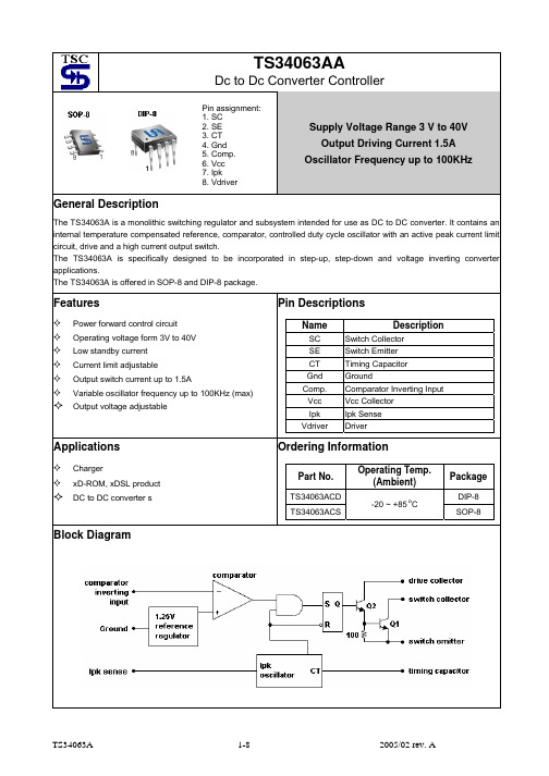
TS34063AADc to Dc Converter ControllerSupply Voltage Range 3 V to 40V Output Driving Current 1.5A Oscillator Frequency up to 100KHzGeneral DescriptionThe TS34063A is a monolithic switching regulator and subsystem intended for use as DC to DC converter. It contains an internal temperature compensated reference, comparator, controlled duty cycle oscillator with an active peak current limit circuit, drive and a high current output switch.The TS34063A is specifically designed to be incorporated in step-up, step-down and voltage inverting converter applications.The TS34063A is offered in SOP-8 and DIP-8 package.FeaturesPower forward control circuit Operating voltage form 3V to 40V Low standby current Current limit adjustable Output switch current up to 1.5AVariable oscillator frequency up to 100KHz (max)Output voltage adjustablePin DescriptionsName DescriptionSC Switch CollectorSE Switch Emitter CT Timing Capacitor Gnd Ground Comp. Comparator Inverting Input Vcc Vcc Collector Ipk Ipk Sense Vdriver DriverApplicationsChargerxD-ROM, xDSL productDC to DC converter sOrdering InformationPart No.Operating Temp.(Ambient)PackageTS34063ACD DIP-8 TS34063ACS-20 ~ +85 oCSOP-8Block DiagramPin assignment:1. SC 2. SE 3. CT 4. Gnd 5. Comp. 6. Vcc 7. Ipk 8. VdriverAbsolute Maximum RatingSupply Voltage V CC 40 V Comparator Input Voltage Range V FB- 0.3 ~ 40 VSwitch Collector Output Voltage V C(SW) 40 V Switch Emitter Voltage V E(SW) 40 V Switch Collector to Emitter Voltage V CE(SW) 40 V Driver Collector Voltage Vc(driver) 40 VDriver Collector Current (note 1) Ic(driver) 100 mAOutput Switching Current I SW 1.5 APower Dissipation DIP-8SOP-8 Pd1.00.5WOperating Junction Temperature Range T J-0 ~ +125 o C Storage Temperature Range T STG-65 ~ +150 o C Note: Maximum package power dissipation limits must be observedElectrical Characteristics (VCC=5V, Ta =25 o C; unless otherwise specified.)Parameter SymbolTestConditionsMinTypMaxUnit Oscillator (OSC)Frequency F OSC C T = 1nF, Vpin5= 0V 24 33 42 KHz Charge Current I CHARGE V CC = 5V ~ 40V -- 30 -- uA Discharge Current I DISCHARGE V CC = 5V ~ 40V -- 200 -- uADischarge to Charge current ratio I DISCHARGE/ I CHARGEPin7 to Vcc -- 6.5 -- --Current Limit Sense Voltage V IPK(SENSE)I DISCHARGE = I CHARGE 250--350mV Output switch (note1)Saturation Voltage V CE(SAT)I SW= 1A, pin1,8 connected) -- 1.0 1.3 VSaturation Voltage V CE(SAT)I SW= 1A, Id=50mA -- 0.45 0.7 VDC current gain H FE I SW = 1A, Vce= 0.5V -- 75 -- --Collector off-state current I C(OFF)Vce= 40V -- 0.01 100 uA ComparatorThreshold Voltae V REF 1.225 1.25 1.275 VLine regulation RegLine V CC = 3V ~ 40V -- -- 6 mVTotal deviceSupply Current I CC V CC = 5V ~ 40V, C T = 1nF,pin7=Vcc, pin5>Vth,pin2=Gnd, remaining pinsopen-- 1.6 3 mANote: 1. Low duty cycle pulse techniques are used during test to maintain junction temperature as close to ambient temperature as possible2. If the output switch is driven into hard saturation (non-Darlington configuration) at low switch currents (<=300mA)and high driver currents (>=30mA), it may take up to 2uS for it to come out of saturation. This condition will shorten the off time at frequencies >= 30KHz, and is magnified at high temperature. This condition does not occur with a Darlington configuration, since the output switch cannot saturate. If a non-Darlington configuration is used, the following output drive condition is recommended:Forced Bata of output switch: Ic output / (Ic driver – 7mA*) >= 10* The 100ohm resistor in the emitter of the driver divide requires about 7mA before the output switch conducts.Circuit DescriptionTypical Application CircuitFigure 7. Step Up ConverterResults Test ConditionsLINE REGULATION Vin= 8V~16V, Io= 175mA 30mV +/- 0.05%Load Regulation Vin= 12V, Io= 75mA to 175mA 10mV +/- 0.017%Output Ripple Vin=12V, Io= 175mA 400mVppEfficiency Vin=12V, Io= 175mA 87.7%Output Ripple with Optional Filter Vin=12V, Io= 175mA 40mVppTypical Application Circuit (continues)Figure 9. Step Down ConverterResults Test ConditionsLine Regulation Vin= 15V~25V, Io= 500mA 12mV +/- 0.12%Load Regulation Vin= 25V, Io= 50mA to 500mA 3mV +/- 0.03%Output Ripple Vin= 25V, Io= 500mA 120mVppShort Circuit Current Vin= 25V, RL= 0.1ohm 1.1AEfficiency Vin= 25V, Io= 500mA 83.7%Output Ripple with Optional Filter Vin= 25V, Io= 500mA 40mVppTypical Application Circuit (continues)Figure 11. Voltage Inverting ConverterResults Test ConditionsLine Regulation Vin= 4.5V~6.0V, Io= 100mA 3mV +/- 0.012%Load Regulation Vin= 5V, Io= 10mA to 100mA 22mV +/- 0.09%Output Ripple Vin= 5V, Io= 100mA 500mVppShort Circuit Current Vin= 5V, RL= 0.1ohm 900mAEfficiency Vin= 5V, Io= 100mA 62.2%Output Ripple with Optional Filter Vin= 5V, Io= 100mA 70mVpp。
CY8CMBR3xxx Family_datasheet_Chinese

CY8CMBR3002, CY8CMBR3102CY8CMBR3106S, CY8CMBR3108CY8CMBR3110, CY8CMBR3116具有SmartSense™自动调试16按键、2个滑条和接近传感器的CapSense®Express™控制器概述CY8CMBR3xxx CapSense®Express™控制器使先进但易于实现的电容触摸用户接口方案成为可能。
该系列寄存器配置型的控制器可支持多达16个电容式感应输入,并消除了设计周期的费时固件开发。
因此,当实现电容按键、滑条和接近感应解决方案时,这些控制需要最小的开发周期时间。
CY8CMBR3xxx系列提供了一个高级模拟检测通道和Capacitive Sigma Delta PLUS (CSD PLUS)感应算法。
该算法会发出高于100:1的信噪比,以确保正确触摸(即使在极端噪声环境中) 通过赛普拉斯SmartSense™自动调试算法来使能这些控制器,能够补偿生产变化造成的影响,并在所有环境条件下动态监控和维持最佳的传感器性能。
另外,通过SmartSense自动调试,在开发和生产过程中,由于可以缩短手动调试工作时间,所以可以加快产品的上市进程。
由于高级性能(如LED亮度控制、接近检测和系统诊断)的优点,可以节省开发时间。
这些控制器通过消除由薄雾、湿气、水滴、液体或流水导致的假触摸使能具有强大耐水性的设计。
CY8CMBR3xxx可包含在小尺寸工业标准封装中。
CY8CMBR3xxx系列系统包括多个开发工具(软件和硬件),能够快速启用用户界面设计。
例如,EZ-Click定制器工具是一个具有简单的图形用户界面的软件,用于通过I2C借口配置器件功能。
该工具还支持CapSense数据阅览,以操控系统性能和支持验证和调试。
另一个工具,Design Toolbox,通过提供设置指南和布局建议简化电路板布局,从而能够优化传感器大小、走线长度和寄生电容。