MC10106FN中文资料
MC100E016FNG,MC10E016FNG,MC100E016FN,MC10E016FN,MC100E016FNR2,MC10E016FNR2, 规格书,Datasheet 资料
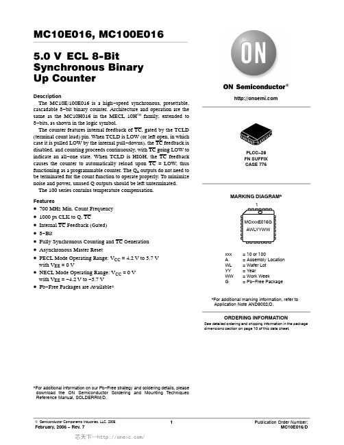
MC10E016, MC100E0165.0 V ECL 8−Bit Synchronous BinaryUp CounterDescriptionThe MC10E/100E016 is a high−speed synchronous, presettable, cascadable 8−bit binary counter. Architecture and operation are the same as the MC10H016 in the MECL 10H™ family, extended to 8−bits, as shown in the logic symbol.The counter features internal feedback of TC, gated by the TCLD (terminal count load) pin. When TCLD is LOW (or left open, in which case it is pulled LOW by the internal pull−downs), the TC feedback is disabled, and counting proceeds continuously, with TC going LOW to indicate an all−one state. When TCLD is HIGH, the TC feedback causes the counter to automatically reload upon TC = LOW, thus functioning as a programmable counter. The Q n outputs do not need to be terminated for the count function to operate properly. To minimize noise and power, unused Q outputs should be left unterminated. The 100 series contains temperature compensation.Features•700 MHz Min. Count Frequency•1000 ps CLK to Q, TC•Internal TC Feedback (Gated)•8−Bit•Fully Synchronous Counting and TC Generation •Asynchronous Master Reset•PECL Mode Operating Range: V CC = 4.2 V to 5.7 Vwith V EE = 0 V•NECL Mode Operating Range: V CC = 0 Vwith V EE = −4.2 V to −5.7 V•Pb−Free Packages are Available**For additional information on our Pb−Free strategy and soldering details, please download the ON Semiconductor Soldering and Mounting Techniques Reference Manual, SOLDERRM/D.MARKING DIAGRAM*xxx= 10 or 100A= Assembly LocationWL= Wafer LotYY= YearWW= Work WeekG=Pb−Free PackagePLCC−28FN SUFFIXCASE 776MCxxxE016GAWLYYWW1*For additional marking information, refer toApplication Note AND8002/D.See detailed ordering and shipping information in the package dimensions section on page 10 of this data sheet.ORDERING INFORMATION1MR CLK TCLD V EE NC P 0P 12627282342524232221201918171615141312115678910PE CE P 7P 6P 5V CCO TC Q 7Q 6V CC Q 5Q 4Q 3P 2P 3P 4V CCO Q 0Q 1Q 2V CCO Figure 1. 28−Lead Pinout Assignment (Top View)All V CC and V CCO pins are tied together on the die.Warning: All V CC , V CCO , and V EE pins must be externally connected to Power Supply to guarantee proper operation.Table 1. PIN DESCRIPTIONPIN FUNCTIONP0−P 7Q 0−Q 7CE PE MR CLK TC TCLD NCV CC , V CCO V EEECL Parallel Data (Preset) Inputs ECL Data OutputsECL Count Enable Control InputECL Parallel Load Enable Control Input ECL Master Reset ECL ClockECL Terminal Count Output ECL TC −Load Control Input No Connect Positive Supply Negative SupplyFigure 2. 8−Bit Binary Counter Logic CounterPE TCLDCEPOMRCLKTable 2. FUNCTION TABLEFUNCTIONCE PE TCLD MR CLK Load Parallel (P n to Q n )X L X L Z Continuous CountL H L L Z Count; Load Parallel on TC = LOW L H H L Z HoldH H X L Z Masters Respond, Slaves Hold X X X L ZZ Reset (Q n : = LOW, TC : = HIGH)XXXHXZ = clock pulse (low to high);ZZ = clock pulse (high to low)Table 3. EXPANDED FUNCTION TABLEFunction PE CE MR TCLD CLK P7−P4P3P2P1P0Q7−Q4Q3Q2Q1Q0TC Load L X L X Z H H H L L H H H L L H Count H L L L Z X X X X X H H H L H HH L L L Z X X X X X H H H H L HH L L L Z X X X X X H H H H H LH L L L Z X X X X X L L L L L H Load L X L X Z H H H L L H H H L L H Hold H H L X Z X X X X X H H H L L HH H L X Z X X X X X H H H L L H Load On H L L H Z H L H H L H H H L H H Terminal H L L H Z H L H H L H H H H L H Count H L L H Z H L H H L H H H H H LH L L H Z H L H H L H L H H L HH L L H Z H L H H L H L H H H HH L L H Z H L H H L H H L L L H Reset X X H X X X X X X X L L L L L HTable 4. ATTRIBUTESCharacteristics ValueInternal Input Pulldown Resistor50 k WInternal Input Pullup Resistor50 k WESD Protection Human Body ModelMachine Model > 2 kV > 200 VMoisture Sensitivity, Indefinite Time Out of Drypack (Note 1)Pb Pkg Pb−Free PkgPLCC−28Level 1Level 3 Flammability Rating Oxygen Index: 28 to 34UL 94 V−0 @ 0.125 in Transistor Count592 DevicesMeets or exceeds JEDEC Spec EIA/JESD78 IC Latchup Test1.For additional information, see Application Note AND8003/D.Table 5. MAXIMUM RATINGSSymbol Parameter Condition 1Condition 2Rating Unit V CC PECL Mode Power Supply V EE = 0 V8VV I PECL Mode Input VoltageNECL Mode Input Voltage V EE = 0 VV CC = 0 VV I V CCV I V EE6−6VI out Output Current ContinuousSurge 50100mAmAT A Operating Temperature Range0 to +85°C T stg Storage Temperature Range−65 to +150°Cq JA Thermal Resistance (Junction−to−Ambient)0 lfpm500 lfpm PLCC−28PLCC−2863.543.5°C/W°C/Wq JC Thermal Resistance (Junction−to−Case)Standard Board PLCC−2822 to 26°C/WT sol Wave Solder PbPb−Free 265265°CMaximum ratings are those values beyond which device damage can occur. Maximum ratings applied to the device are individual stress limit values (not normal operating conditions) and are not valid simultaneously. If these limits are exceeded, device functional operation is not implied, damage may occur and reliability may be affected.Table 6. 10E SERIES PECL DC CHARACTERISTICS V CCx = 5.0 V; V EE = 0.0 V (Note 1)0°C25°C85°CSymbol Characteristic Min Typ Max Min Typ Max Min Typ Max Unit I EE Power Supply Current151181151181151181mA V OH Output HIGH Voltage (Note 2)398040704160402041054190409041854280mV V OL Output LOW Voltage (Note 2)305032103370305032103370305032273405mV V IH Input HIGH Voltage383039954160387040304190394041104280mV V IL Input LOW Voltage305032853520305032853520305033023555mV I IH Input HIGH Current150150150m AI IL Input LOW Current0.50.30.50.250.30.2m A NOTE:Device will meet the specifications after thermal equilibrium has been established when mounted in a test socket or printed circuit board with maintained transverse airflow greater than 500 lfpm. Electrical parameters are guaranteed only over the declaredoperating temperature range. Functional operation of the device exceeding these conditions is not implied. Device specification limit values are applied individually under normal operating conditions and not valid simultaneously.1.Input and output parameters vary 1:1 with V CC. V EE can vary −0.46 V / +0.06 V.2.Outputs are terminated through a 50 W resistor to V CC− 2.0 V.Symbol Characteristic Min Typ Max Min Typ Max Min Typ Max Unit I EE Power Supply Current151181151181151181mA V OH Output HIGH Voltage (Note 4)−1020−930−840−980−895−810−910−815−720mV V OL Output LOW Voltage (Note 4)−1950−1790−1630−1950−1790−1630−1950−1773−1595mV V IH Input HIGH Voltage−1170−1005−840−1130−970−810−1060−890−720mV V IL Input LOW Voltage−1950−1715−1480−1950−1715−1480−1950−1698−1445mV I IH Input HIGH Current150150150m A I IL Input LOW Current0.50.30.50.0650.30.2m A NOTE:Device will meet the specifications after thermal equilibrium has been established when mounted in a test socket or printed circuit board with maintained transverse airflow greater than 500 lfpm. Electrical parameters are guaranteed only over the declared operating temperature range. Functional operation of the device exceeding these conditions is not implied. Device specification limit values are applied individually under normal operating conditions and not valid simultaneously.3.Input and output parameters vary 1:1 with V CC. V EE can vary −0.46 V / +0.06 V.4.Outputs are terminated through a 50 W resistor to V CC− 2.0 V.Table 8. 100E SERIES PECL DC CHARACTERISTICS V CCx = 5.0 V; V EE = 0.0 V(Note 5)Symbol Characteristic0°C25°C85°CUnit Min Typ Max Min Typ Max Min Typ MaxI EE Power Supply Current151181151181174208mA V OH Output HIGH Voltage (Note 6)397540504120397540504120397540504120mV V OL Output LOW Voltage (Note 6)319032953380319032553380319032603380mV V IH Input HIGH Voltage383539754120383539754120383539754120mV V IL Input LOW Voltage319033553525319033553525319033553525mV I IH Input HIGH Current150150150m A I IL Input LOW Current0.50.30.50.250.50.2m A NOTE:Device will meet the specifications after thermal equilibrium has been established when mounted in a test socket or printed circuit board with maintained transverse airflow greater than 500 lfpm. Electrical parameters are guaranteed only over the declared operating temperature range. Functional operation of the device exceeding these conditions is not implied. Device specification limit values are applied individually under normal operating conditions and not valid simultaneously.5.Input and output parameters vary 1:1 with V CC. V EE can vary −0.46 V / +0.8 V.6.Outputs are terminated through a 50 W resistor to V CC− 2.0 V.Symbol Characteristic Min Typ Max Min Typ Max Min Typ Max Unit I EE Power Supply Current151181151181174208mA V OH Output HIGH Voltage (Note 8)−1025−950−880−1025−950−880−1025−950−880mV V OL Output LOW Voltage (Note 8)−1810−1705−1620−1810−1745−1620−1810−1740−1620mV V IH Input HIGH Voltage−1165−1025−880−1165−1025−880−1165−1025−880mV V IL Input LOW Voltage−1810−1645−1475−1810−1645−1475−1810−1645−1475mV I IH Input HIGH Current150150150m A I IL Input LOW Current0.50.30.50.250.50.2m A NOTE:Device will meet the specifications after thermal equilibrium has been established when mounted in a test socket or printed circuit board with maintained transverse airflow greater than 500 lfpm. Electrical parameters are guaranteed only over the declared operating temperature range. Functional operation of the device exceeding these conditions is not implied. Device specification limit values are applied individually under normal operating conditions and not valid simultaneously.7.Input and output parameters vary 1:1 with V CC. V EE can vary −0.46 V / +0.8 V.8.Outputs are terminated through a 50 W resistor to V CC− 2.0 V.Table 10. AC CHARACTERISTICS V CCx= 5.0 V; V EE = 0.0 V or V CCx = 0.0 V; V EE = −5.0 V (Note 9)0°C25°C85°CSymbol Characteristic Min Typ Max Min Typ Max Min Typ Max Unit f MAX Maximum Toggle Frequency700700700MHz f COUNT Maximum Count Frequency700900700900700900MHz t PLH, t PHL Propagation Delay to Output psCLK to Q500725900500725900500725900MR to Q500775900500775900500775900CLK to TC500775900500775900500775900MR to TC500775900500775900500775900t s Setup Time (to CLK +)psPn150−30150−30150−30CE600400600400600400PE600400600400600400TCLD500300500300500300t h Hold Time (to CLK +)Pn350100350100350100CE400200400200400200PE020*********TCLD100−300100−300100−300t RR Reset Recovery Time900700900700900700ps t PW Minimum Pulse Width psCLK, MR400400400t JITTER Random Clock Jitter (RMS)< 1< 1< 1ps t r, t f Rise/Fall Times (20 − 80%)200510700200510700200510700ps NOTE:Device will meet the specifications after thermal equilibrium has been established when mounted in a test socket or printed circuit board with maintained transverse airflow greater than 500 lfpm. Electrical parameters are guaranteed only over the declared operating temperature range. Functional operation of the device exceeding these conditions is not implied. Device specification limit values are applied individually under normal operating conditions and not valid simultaneously.9.10 Series: V EE can vary −0.46 V / +0.06 V.100 Series: V EE can vary −0.46 V / +0.8 V.APPLICATIONS INFORMATIONCascading Multiple E016 DevicesFor applications which call for larger than 8−bit counters multiple E016s can be tied together to achieve very wide bit width counters. The active low terminal count (TC) output and count enable input (CE) greatly facilitate the cascading of E016 devices. Two E016s can be cascaded without the need for external gating, however for counters wider than 16bits external OR gates are necessary for cascade implementations.Figure 3 below pictorially illustrates the cascading of 4E016s to build a 32−bit high frequency counter. Note the E101 gates used to OR the terminal count outputs of the lower order E016s to control the counting operation of the higher order bits. When the terminal count of the preceding device (or devices) goes low (the counter reaches an all 1s state) the more significant E016 is set in its count mode and will count one binary digit upon the next positive clock transition. In addition, the preceding devices will also count one bit thus sending their terminal count outputs back to a high state disabling the count operation of the more significant counters and placing them back into hold modes.Therefore, for an E016 in the chain to count, all of the lower order terminal count outputs must be in the low state. The bit width of the counter can be increased or decreased by simply adding or subtracting E016 devices from Figure 3 and maintaining the logic pattern illustrated in the same figure.The maximum frequency of operation for the cascaded counter chain is set by the propagation delay of the TC output and the necessary setup time of the CE input and the propagation delay through the OR gate controlling it (for 16−bit counters the limitation is only the TC propagation delay and the CE setup time). Figure 3 shows EL01 gates used to control the count enable inputs, however, if the frequency of operation is lower a slower, ECL OR gate can be used. Using the worst case guarantees for these parameters from the ECLinPS data book, the maximum count frequency for a greater than 16−bit counter is 500 MHz and that for a 16−bit counter is 625 MHz.Note that this assumes the trace delay between the TC outputs and the CE inputs are negligible. If this is not the case estimates of these delays need to be added to the calculations.Figure 3. 32−Bit Cascaded E016 CounterCLOCKLOADProgrammable DividerThe E016 has been designed with a control pin which makes it ideal for use as an 8−bit programmable divider. The TCLD pin (load on terminal count) when asserted reloads the data present at the parallel input pin (Pn’s) upon reaching terminal count (an all 1s state on the outputs). Because this feedback is built internal to the chip, the programmable division operation will run at very nearly the same frequency as the maximum counting frequency of the device. Figure 4below illustrates the input conditions necessary for utilizing the E016 as a programmable divider set up to divide by 113.Figure 4. Mod 2 to 256 Programmable Divider To determine what value to load into the device to accomplish the desired division, the designer simply subtracts the binary equivalent of the desired divide ratio from the binary value for 256. As an example for a divide ratio of 113:Pn’s = 256 − 113 = 8F 16 = 1000 1111where:P0 = LSB and P7 = MSBForcing this input condition as per the setup in Figure 4will result in the waveforms of Figure 5. Note that the TC output is used as the divide output and the pulse duration isequal to a full clock period. For even divide ratios, twice the desired divide ratio can be loaded into the E016 and the TC output can feed the clock input of a toggle flip flop to create a signal divided as desired with a 50% duty cycle.Table 11. Preset Values for Various Divide RatiosDivide Ratio Preset Data Inputs P7P6P5P4P3P2P1P02H H H H H HH L 3H H H H H H L H 4H H H H H H L L 5H H H H H L H H w w •••••••w ••••••••112H L L H L L L L 113H L L L H H H H 114H L L L H H H L ••••••••••••••••••254L L L L L L H L 255L L L L L L L H 256LLLLLLLLA single E016 can be used to divide by any ratio from 2to 256 inclusive. If divide ratios of greater than 256 are needed multiple E016s can be cascaded in a manner similar to that already discussed. When E016s are cascaded to build larger dividers the TCLD pin will no longer provide a means for loading on terminal count. Because one does not want to reload the counters until all of the devices in the chain have reached terminal count, external gating of the TC pins must be used for multiple E016 divider chains.PEClockTCFigure 5. Divide by 113 E016 Programmable Divider WaveformsFigure 6. 32−Bit Cascaded E016 Programmable DividerFigure 6 shows a typical block diagram of a 32−bit divider chain. Once again to maximize the frequency of operation EL01 OR gates were used. For lower frequency applications a slower OR gate could replace the EL01. Note that for a 16−bit divider the OR function feeding the PE (program enable) input CANNOT be replaced by a wire OR tie as the TC output of the least significant E016 must also feed the CE input of the most significant E016. If the two TC outputs were OR tied the cascaded count operation would not operate properly. Because in the cascaded form the PE feedback is external and requires external gating, the maximum frequency of operation will be significantly less than the same operation in a single device.Maximizing E016 Count FrequencyThe E016 device produces 9 fast transitioning single−ended outputs, thus V CC noise can become significant in situations where all of the outputs switch simultaneously in the same direction. This V CC noise can negatively impact the maximum frequency of operation of the device. Since the device does not need to have the Q outputs terminated to count properly, it is recommended that if the outputs are not going to be used in the rest of the system they should be left unterminated. In addition, if only a subset of the Q outputs are used in the system only those outputs should be terminated. Not terminating the unused outputs will not only cut down the V CC noise generated but will also save in total system power dissipation. Following these guidelines will allow designers to either be more aggressive in their designs or provide them with an extra margin to the published data book specifications.Figure 7. Typical Termination for Output Driver and Device Evaluation (See Application Note AND8020/D − Termination of ECL Logic Devices.)V TTV TT = V CC − 2.0 VORDERING INFORMATIONDevicePackage Type Shipping †MC10E016FN PLCC −2837 Units/Rail MC10E016FNG PLCC −28(Pb −Free)37 Units/Rail MC10E016FNR2PLCC −28500 Units/Reel MC10E016FNR2G PLCC −28(Pb −Free)500 Units/Reel MC100E016FN PLCC −2837 Units/Rail MC100E016FNG PLCC −28(Pb −Free)37 Units/Rail MC100E016FNR2PLCC −28500 Units/Reel MC100E016FNR2GPLCC −28(Pb −Free)500 Units/Reel†For information on tape and reel specifications, including part orientation and tape sizes, please refer to our Tape and Reel Packaging Specifications Brochure, BRD8011/D.PACKAGE DIMENSIONSPLCC−28FN SUFFIXPLASTIC PLCC PACKAGECASE 776−02ISSUE ESMALLER THAN 0.025 (0.635).11MECL is a trademark of Motorola, Inc.ON Semiconductor and are registered trademarks of Semiconductor Components Industries, LLC (SCILLC). SCILLC reserves the right to make changes without further notice to any products herein. SCILLC makes no warranty, representation or guarantee regarding the suitability of its products for any particular purpose, nor does SCILLC assume any liability arising out of the application or use of any product or circuit, and specifically disclaims any and all liability, including without limitation special, consequential or incidental damages.“Typical” parameters which may be provided in SCILLC data sheets and/or specifications can and do vary in different applications and actual performance may vary over time. All operating parameters, including “Typicals” must be validated for each customer application by customer’s technical experts. SCILLC does not convey any license under its patent rights nor the rights of others. SCILLC products are not designed, intended, or authorized for use as components in systems intended for surgical implant into the body, or other applications intended to support or sustain life, or for any other application in which the failure of the SCILLC product could create a situation where personal injury or death may occur. Should Buyer purchase or use SCILLC products for any such unintended or unauthorized application, Buyer shall indemnify and hold SCILLC and its officers, employees, subsidiaries, affiliates, and distributors harmless against all claims, costs, damages, and expenses, and reasonable attorney fees arising out of, directly or indirectly, any claim of personal injury or death associated with such unintended or unauthorized use, even if such claim alleges that SCILLC was negligent regarding the design or manufacture of the part. SCILLC is an Equal Opportunity/Affirmative Action Employer. This literature is subject to all applicable copyright laws and is not for resale in any manner.PUBLICATION ORDERING INFORMATION。
12CWQ06FN中文资料

CT Typ. Junction Capacitance (Per Leg)
LS Typical Series Inductance (Per Leg)
(1) Pulse Width < 300µs,.61 0.79 0.57
0.72 3 35
0.36 24.14 360
(Per Leg)
10
10 0 10 20 30 40 50 60 70
Reverse V oltag e - V R (V ) Fig. 3 - Typical Junction Capacitance
Vs. Reverse Voltage (Per Leg)
Therm al Im pedance Z thJC ( C/W )
1000
T J= 25 C 100
Junction Capacitance - C T (pF)
1 0.2 0.4 0.6 0.8 1 1.2 1.4 1.6 1.8 2 2.2 2.4
Forward Voltage Drop - VFM (V) Fig. 1 - Max. Forward Voltage Drop Characteristics
320
Surge Current * See Fig. 7
105
EAS Non-Repet.Avalan.Energy(PerLeg)
7
IAR RepetitiveAvalancheCurrent
0.8
(Per Leg)
A 50% duty cycle @ TC = 131°C, rectangular wave form
VRRM
12
A
60
V
IFSM @ tp = 5 µs sine
NFE61PTxxx资料

For High Speed Signal
For Standard (Low DC
Resistance Type)
For Standard
0603
For High Speed Signal (Sharp impedance characteristics)
* Please see P.58 "Derating of Rated Current".
60 (0.5A) 60 (3A)
50 (3A)
60 (6A)
33 (3A) 30 (1A)
30 (3A)
33 (6A)
22 22
10 10 10
10 10
555
mm 0603 1005 1608 2012 1005 1608 2012 1608 2012
EIA Code 0201 0402 0603 0805 0402 0603 0805 0603 0805
47 47
1800
1000 (1.5A) 1000
1000
1
600 (1.5A)
600
600
470 (2A)
470
390 (2A)
390
330 (1.5A)
330
220 (2A)
220
220
180 (1.5A)
180 (3A)
120 (2A)
120 (3A)
120
120
100
80 (1A)
75 (3A)
4516 1806
1005
1608
0402
0603
GHz Range Noise GHz Range Noise Suppression Type Suppression Type BLM15H/E BLM18H/E/G
mc6a遥控器使用说明书(范本)
mc6a遥控器使用说明书mc6a遥控器使用说明书篇一:MC6中文说明 FHSS USER M ANUAL 6ChannelTransmit ter(6通发射机) Chann el 5(5通道) Chann el 6(6通道) Thrott le Trim(油门微调) Ru dder Tri m (方向微调) Elevat or Trim(升降微调)(副翼微调) Ail eron Tri m V-tail ElevonMix On V-tail On ( V尾混控) OnOff s ith 电源开关 Sithesin upper positio n Revers es diret ion(通道反向) of han nels1-4Elevon Off(三角翼混控) V-tai l Elevon Mix Off混控开关 Si thes inloerpos ition No rmal dir etion(通道正向) of h annels 1-4 FHSS This 4GHZfeatures a uniqu e odingprotoolto use t his Tran smitterith a re eiver it must be bound t o the re eiver. T he fator ill bin d the tr ansmitte r to the reeiver but sho uld it b ee unbou nd or sh ould oupurhasea seondreeiverthen ple ase foll o the pr oedure o utlinedbelo. (发射机和接收机需绑定。
MC10EP16T资料

MC10EP16T, MC100EP16T 3.3V / 5VĄECL Differential Receiver/Driver with Internal TerminationThe EP16T is a world–class differential receiver/driver. The device is functionally equivalent to the EP16 with internal termination resistors. A 50 W resistor is connected from the D input to the VT pin and from the D input to the VT pin. Tie the VT and VT pins to VTT supply (V CC – 2 V) for parallel termination or connect VT and VT pins for 100 W input series termination.Special considerations are required for differential inputs under No Signal conditions to prevent instability.The 100 Series contains temperature compensation.•220 ps Typical Propagation Delay •Maximum Frequency > 3 GHz Typical•PECL Mode Operating Range: V CC = 3.0 V to 5.5 V with V EE = 0 V•NECL Mode Operating Range: V CC = 0 V with V EE = –3.0 V to –5.5 V•Internal 50 W Termination ResistorsDevice Package Shipping ORDERING INFORMATIONMC10EP16TD SO–898 Units/Rail MC10EP16TDR2SO–82500 Tape & Reel MC100EP16TD SO–898 Units/Rail MC100EP16TDR2SO–82500 Tape & Reel MC10EP16TDT TSSOP–8100 Units/Rail MC10EP16TDTR2TSSOP–82500 Tape & Reel MC100EP16TDTTSSOP–8100 Units/Rail MC100EP16TDTR2TSSOP–82500 Tape & ReelQV EEV CCFigure 1. 8–Lead Pinout (Top View) and Logic DiagramD QD VT VT PIN DESCRIPTION1.For additional information, see Application Note AND8003/D.MAXIMUM RATINGS (Note 2)circuit is in a test socket or mounted on a printed circuit board and transverse airflow greater than 500 lfpm is maintained.3.Input and output parameters vary 1:1 with V CC. V EE can vary +0.3 V to –2.2 V.4.All loading with 50 W to V CC–2.0 volts.5.V IHCMR min varies 1:1 with V EE, V IHCMR max varies 1:1 with V CC. The V IHCMR range is referenced to the most positive side of the differentialinput signal.circuit is in a test socket or mounted on a printed circuit board and transverse airflow greater than 500 lfpm is maintained.6.Input and output parameters vary 1:1 with V CC. V EE can vary +2.0 V to –0.5 V.7.All loading with 50 W to V CC–2.0 volts.8.V IHCMR min varies 1:1 with V EE, V IHCMR max varies 1:1 with V CC. The V IHCMR range is referenced to the most positive side of the differentialinput signal.circuit is in a test socket or mounted on a printed circuit board and transverse airflow greater than 500 lfpm is maintained.9.Input and output parameters vary 1:1 with V CC.10.All loading with 50 W to V CC–2.0 volts.11.V IHCMR min varies 1:1 with V EE, V IHCMR max varies 1:1 with V CC. The V IHCMR range is referenced to the most positive side of the differentialinput signal.circuit is in a test socket or mounted on a printed circuit board and transverse airflow greater than 500 lfpm is maintained.12.Input and output parameters vary 1:1 with V CC. V EE can vary +0.3 V to –2.2 V.13.All loading with 50 W to V CC–2.0 volts.14.V IHCMR min varies 1:1 with V EE, V IHCMR max varies 1:1 with V CC. The V IHCMR range is referenced to the most positive side of the differentialinput signal.circuit is in a test socket or mounted on a printed circuit board and transverse airflow greater than 500 lfpm is maintained.15.Input and output parameters vary 1:1 with V CC. V EE can vary +2.0 V to –0.5 V.16.All loading with 50 W to V CC–2.0 volts.17.V IHCMR min varies 1:1 with V EE, V IHCMR max varies 1:1 with V CC. The V IHCMR range is referenced to the most positive side of the differentialinput signal.circuit is in a test socket or mounted on a printed circuit board and transverse airflow greater than 500 lfpm is maintained.18.Input and output parameters vary 1:1 with V CC.19.All loading with 50 W to V CC–2.0 volts.20.V IHCMR min varies 1:1 with V EE, V IHCMR max varies 1:1 with V CC. The V IHCMR range is referenced to the most positive side of the differentialinput signal.AC CHARACTERISTICS V= 0 V; V = –3.0 V to –5.5 V or V = 3.0 V to 5.5 V; V = 0 V (Note 21)CC 22.Skew is measured between outputs under identical transitions. Duty cycle skew is defined only for differential operation when the delays are measured from the cross point of the inputs to the cross point of the outputs.10020030040050060070080090005001000150020002500300035004000Figure 2. F max /JitterFREQUENCY (MHz)V O U T p p (m V )V TTV TT=V CC– 2.0 VFigure 3. Typical Termination for Output Driver and Device Evaluation(See Application Note AND8020 – Termination of ECL Logic Devices.)Resource Reference of Application NotesAN1404–ECLinPS Circuit Performance at Non–Standard V IH LevelsAN1405–ECL Clock Distribution TechniquesAN1406–Designing with PECL (ECL at +5.0 V)AN1504–Metastability and the ECLinPS FamilyAN1568–Interfacing Between LVDS and ECLAN1650–Using Wire–OR Ties in ECLinPS DesignsAN1672–The ECL Translator GuideAND8001–Odd Number Counters DesignAND8002–Marking and Date CodesAND8009–ECLinPS Plus Spice I/O Model KitAND8020–Termination of ECL Logic DevicesFor an updated list of Application Notes, please see our website at .PACKAGE DIMENSIONSSO–8D SUFFIX PLASTIC SOIC PACKAGECASE 751–07NOTES:1.DIMENSIONING AND TOLERANCING PER ANSIY14.5M, 1982.2.CONTROLLING DIMENSION: MILLIMETER.3.DIMENSION A AND B DO NOT INCLUDE MOLDPROTRUSION.4.MAXIMUM MOLD PROTRUSION 0.15 (0.006) PERSIDE.5.DIMENSION D DOES NOT INCLUDE DAMBARPROTRUSION. ALLOWABLE DAMBARPROTRUSION SHALL BE 0.127 (0.005) TOTAL INEXCESS OF THE D DIMENSION AT MAXIMUMMATERIAL CONDITION.6.751-01 THRU 751-06 ARE OBSOLETE. NEWSTANDAARD IS 751-07DIMAMIN MAX MIN MAXINCHES4.805.000.1890.197MILLIMETERSB 3.80 4.000.1500.157C 1.35 1.750.0530.069D0.330.510.0130.020G 1.27 BSC0.050 BSCH0.100.250.0040.010J0.190.250.0070.010K0.40 1.270.0160.050M0 8 0 8N0.250.500.0100.020S 5.80 6.200.2280.244 YM0.25 (0.010)Z S X S____DIM MIN MAX MIN MAXINCHESMILLIMETERSA 2.90 3.100.1140.122B 2.90 3.100.1140.122C0.80 1.100.0310.043D0.050.150.0020.006F0.400.700.0160.028G0.65 BSC0.026 BSCL 4.90 BSC0.193 BSCM0 6 0 6____K0.250.400.0100.016TSSOP–8DT SUFFIXPLASTIC TSSOP PACKAGECASE 948R–02ISSUE ANOTES:1.DIMENSIONING AND TOLERANCING PER ANSIY14.5M, 1982.2.CONTROLLING DIMENSION: MILLIMETER.3.DIMENSION A DOES NOT INCLUDE MOLD FLASH.PROTRUSIONS OR GATE BURRS. MOLD FLASHOR GATE BURRS SHALL NOT EXCEED 0.15(0.006) PER SIDE.4.DIMENSION B DOES NOT INCLUDE INTERLEADFLASH OR PROTRUSION. INTERLEAD FLASH ORPROTRUSION SHALL NOT EXCEED 0.25 (0.010)PER SIDE.5.TERMINAL NUMBERS ARE SHOWN FORREFERENCE ONLY.6.DIMENSION A AND B ARE TO BE DETERMINEDAT DATUM PLANE -W-.ON Semiconductor and are registered trademarks of Semiconductor Components Industries, LLC (SCILLC). SCILLC reserves the right to make changes without further notice to any products herein. SCILLC makes no warranty, representation or guarantee regarding the suitability of its products for any particular purpose, nor does SCILLC assume any liability arising out of the application or use of any product or circuit, and specifically disclaims any and all liability, including without limitation special, consequential or incidental damages. “Typical” parameters which may be provided in SCILLC data sheets and/or specifications can and do vary in different applications and actual performance may vary over time. All operating parameters, including “Typicals” must be validated for each customer application by customer’s technical experts. SCILLC does not convey any license under its patent rights nor the rights of others.SCILLC products are not designed, intended, or authorized for use as components in systems intended for surgical implant into the body, or other applications intended to support or sustain life, or for any other application in which the failure of the SCILLC product could create a situation where personal injury or death may occur. Should Buyer purchase or use SCILLC products for any such unintended or unauthorized application, Buyer shall indemnify and hold SCILLC and its officers, employees, subsidiaries, affiliates, and distributors harmless against all claims, costs, damages, and expenses, and reasonable attorney fees arising out of, directly or indirectly, any claim of personal injury or death associated with such unintended or unauthorized use, even if such claim alleges that SCILLC was negligent regarding the design or manufacture of the part. SCILLC is an Equal Opportunity/Affirmative Action Employer. PUBLICATION ORDERING INFORMATIONJAPAN: ON Semiconductor, Japan Customer Focus Center2–9–1 Kamimeguro, Meguro–ku, Tokyo, Japan 153–0051Phone: 81–3–5773–3850Email: r14525@。
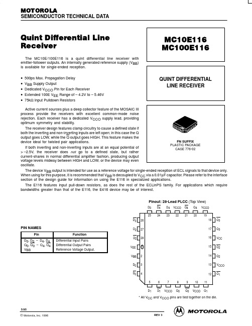
MC100E116FN中文资料
* All VCC and VCCO pins are tied together on the die.
5/95
© Motorola, Inc. 1996
2–1
R16 MC100E116
LOGIC DIAGRAM
D0 D0 D1 D1 D2 D2 D3 D3 D4 D4 VBB Q0 Q0 Q1 Q1 Q2 Q2 Q3 Q3 Q4 Q4
0.007 (0.180) U T L –M
M
B -NY BRK
M
S
N
S S
0.007 (0.180)
T L –M
N
S
D Z -L-M-
W
28 1
D X VIEW D-D G1 0.010 (0.250)
S
V
T L –M
S
N
S
A Z R
0.007 (0.180) 0.007 (0.180)
M
T L –M T L –M
S
N N
S
H
S
0.007 (0.180)
M
T L –M
S
N
S
M
S
C
E G G1 0.010 (0.250)
S
K1 0.004 (0.100) J -TSEATING PLANE
K F VIEW S 0.007 (0.180)
M
VIEW S T L –M
S
T L –M
S
N
S
N
S
NOTES: 1. DATUMS -L-, -M-, AND -N- DETERMINED WHERE TOP OF LEAD SHOULDER EXITS PLASTIC BODY AT MOLD PARTING LINE. 2. DIM G1, TRUE POSITION TO BE MEASURED AT DATUM -T-, SEATING PLANE. 3. DIM R AND U DO NOT INCLUDE MOLD FLASH. ALLOWABLE MOLD FLASH IS 0.010 (0.250) PER SIDE. 4. DIMENSIONING AND TOLERANCING PER ANSI Y14.5M, 1982. 5. CONTROLLING DIMENSION: INCH. 6. THE PACKAGE TOP MAY BE SMALLER THAN THE PACKAGE BOTTOM BY UP TO 0.012 (0.300). DIMENSIONS R AND U ARE DETERMINED AT THE OUTERMOST EXTREMES OF THE PLASTIC BODY EXCLUSIVE OF MOLD FLASH, TIE BAR BURRS, GATE BURRS AND INTERLEAD FLASH, BUT INCLUDING ANY MISMATCH BETWEEN THE TOP AND BOTTOM OF THE PLASTIC BODY. 7. DIMENSION H DOES NOT INCLUDE DAMBAR PROTRUSION OR INTRUSION. THE DAMBAR PROTRUSION(S) SHALL NOT CAUSE THE H DIMENSION TO BE GREATER THAN 0.037 (0.940). THE DAMBAR INTRUSION(S) SHALL NOT CAUSE THE H DIMENSION TO BE SMALLER THAN 0.025 (0.635).
MC100系列说明书(DOC)

MC100系列智能多媒体控制系统Intelligent Multimedia Control System(适用于MC100系列机型)用户安装手册User’s Manual* *请在安装使用前认真阅读本说明书**尊敬的用户:感谢您选购我们生产的这个系列多媒体中央控制器。
该产品具有外观设计小巧高档大方;使用简单方便;功能强大;可直接外接其他厂家的设备;二个可编程232口最多可同时控制两个不同厂家的投影机或其他设备;可对各接口重新定义和单独控制;投影机一键切换;投影幕自动升降;开机即是电脑画面等等多种实用功能。
为了您能安全地使用本设备,发挥其最大的功能,强烈建议在安装使用前先仔细阅读本说明书。
若有任何技术问题或对产品的意见和建议,请与本公司技术服务部联系。
联系方法如下:电话:(020)33534881 61087188传真:(020)61087188-8002地址:广州市天河软件园建工路9号4楼南区A1邮编:510665E-mail:laitong@http://特别提醒:1. 在使用本系统的时候,严禁在开机时对各个部件进行插拔(特别是通讯口及VGA接口,这可能会人为损坏设备)。
2. 本控制器为智能开关设计,在雷雨天气或长时间不使用时,请关闭电源总闸。
3. 本控制器内有强电模块,严禁带电自行维修。
4.因中控本身已做好接地处理,为有效保护中控及设备,请在强电输入部分做好接地措施!目录一.系统说明1,中控简介 (5)2,简单使用说明 (5)二,硬件连接1,连线说明 (6)三,系统设置1,系统通讯协议 (8)2,开机状态设置 (10)3,开关机流程设置 (11)4,开关延时设置 (12)5,投影机设置 (12)6,红外学习 (14)7,按键面板设置 (15)8,其它设置 (16)四,常见故障处理1,按控制面板“系统开”无法开机 (18)2,红外学习不成功或显示成功却不能遥控 (18)3,有些设备红外遥控不灵 (19)4,投影机打不开 (19)5,中控与电脑连接失败 (19)一、系统说明1. 中控简介智能多媒体控制器为简单电化教室、会议室及家居提供了很好的解决方案。
50WQ06FN中文资料

SCHOTTKY RECTIFIER5.5 Amp50WQ06FNBulletin PD-20525 rev. E 03/03D-Pak (TO-252AA)50WQ06FNBulletin PD-20525 rev. E 03/032Part number50WQ06FNV RMax. DC Reverse Voltage (V)V RWM Max. Working Peak Reverse Voltage (V)Voltage RatingsV FMMax. Forward Voltage Drop 0.57V @ 5A * See Fig. 1(1)0.74V @ 10A 0.54V @ 5A 0.68V @ 10A I RMMax. Reverse Leakage Current 3mA T J = 25 °C * See Fig. 2(1)35mA T J = 125 °CV F(TO)Threshold Voltage 0.35VT J = T J max.r t Forward Slope Resistance 25.5m ΩC T Typical Junction Capacitance 360pF V R = 5V DC , (test signal range 100Khz to 1Mhz) 25 °C L STypical Series Inductance5.0nH Measured lead to lead 5mm from package body dv/dt Max. Voltage Rate of Change10000V/µs(Rated V R )T J = 25 °C T J = 125 °C V R = rated V RElectrical SpecificationsParameters50WQ...UnitsConditions(1) Pulse Width < 300µs, Duty Cycle < 2%T J Max. Junction Temperature Range(*)-40 to 150°C T stgMax. Storage Temperature Range-40 to 150°CR thJC Max. Thermal Resistance Junction3.0°C/W DC operation * See Fig. 4to Case wtApproximate Weight 0.3 (0.01)g (oz.)Case StyleD - PAKSimilar to TO-252AAThermal-Mechanical SpecificationsParameters50WQ...UnitsConditions60I F(AV)Max. Average Forward Current5.5A50% duty cycle @ T C = 132°C, rectangular wave form* See Fig. 5I FSM Max. Peak One Cycle Non-Repetitive 3205µs Sine or 3µs Rect. pulse Surge Current * See Fig. 710510ms Sine or 6ms Rect. pulseE AS Non-Repetitive Avalanche Energy 7mJ T J = 25 °C, I AS = 1.2 Amps, L = 10 mHI ARRepetitive Avalanche Current0.8ACurrent decaying linearly to zero in 1 µsecFrequency limited by T J max. V A = 1.5 x V R typicalAbsolute Maximum RatingsFollowing any rated load condition and with rated V RRM appliedA Parameters50WQ... UnitsConditions< thermal runaway condition for a diode on its own heatsink (*) dPtot1dTjRth( j-a)50WQ06FN3 50WQ06FNBulletin PD-20525 rev. E 03/03 450WQ06FN5 5K3A712A50WQ06FNBulletin PD-20525 rev. E 03/03 6IR WORLD HEADQUARTERS: 233 Kansas St., El Segundo, California 90245, USA Tel: (310) 252-7105TAC Fax: (310) 252-7309Visit us at for sales contact information. 03/03。
- 1、下载文档前请自行甄别文档内容的完整性,平台不提供额外的编辑、内容补充、找答案等附加服务。
- 2、"仅部分预览"的文档,不可在线预览部分如存在完整性等问题,可反馈申请退款(可完整预览的文档不适用该条件!)。
- 3、如文档侵犯您的权益,请联系客服反馈,我们会尽快为您处理(人工客服工作时间:9:00-18:30)。
0.007 (0.180) M T L–M U
S
N
S S
0.007 (0.180) M T L–M
N
S
20
1
X V VIEW D–D
G1
0.010 (0.250)
S
T L–M
S
N
S
A Z R
0.007 (0.180) M T L–M 0.007 (0.180) M T L–M
S
N N
S
S
S
H
0.007 (0.180) M T L–M
VCC1 BOUT 1 2 3 4 5 6 7 8 16 15 14 13 12 11 10 9 VCC2 COUT CIN CIN CIN BIN BIN BIN
15
VCC1 = PIN 1 VCC2 = PIN 16 VEE = PIN 8
AOUT AIN AIN AIN AIN VEE
Pin assignment is for Dual–in–Line Package. For PLCC pin assignment, see the Pin Conversion Tables on page 6–11 of the Motorola MECL Data Book (DL122/D).
Logic 1 Logic 0 Logic 1 Logic 0 (50Ω Load)
VOH VOL VOHA VOLA
(20 to 80%) (20 to 80%)
ELECTRICAL CHARACTERISTICS (continued)
TEST VOLTAGE VALUES (Volts) @ Test Temperature –30°C +25°C +85°C Pin Under Test 8 4 4 3 2 3 2 3 2 3 2 4 9 Pulse In t4+3– t4–3+ (20 to 80%) t3+ 3 3 3 4 4 4 Pulse Out 3 3 3 4 9 4 9 4 4 VIHmax –0.890 –0.810 –0.700 VILmin –1.890 –1.850 –1.825 VIHAmin –1.205 –1.105 –1.035 VILAmax –1.500 –1.475 –1.440 VEE –5.2 –5.2 –5.2 (VCC) Gnd 1, 16 1, 16 1, 16 1, 16 1, 16 1, 16 1, 16 1, 16 1, 16 1, 16 1, 16 +2.0 V 1, 16 1, 16 1, 16
MOTOROLA
3–28
MECL Data DL122 — Rev 6
元器件交易网
MC10106
OUTLINE DIMENSIONS
L SUFFIX CERAMIC DIP PACKAGE CASE 620–10 ISSUE V
9
–A–
16
–B–
1 8
C
L
NOTES: 1. DIMENSIONING AND TOLERANCING PER ANSI Y14.5M, 1982. 2. CONTROLLING DIMENSION: INCH. 3. DIMENSION L TO CENTER OF LEAD WHEN FORMED PARALLEL. 4. DIMENSION F MAY NARROW TO 0.76 (0.030) WHERE THE LEAD ENTERS THE CERAMIC BODY. DIM A B C D E F G H K L M N INCHES MIN MAX 0.750 0.785 0.240 0.295 ––– 0.200 0.015 0.020 0.050 BSC 0.055 0.065 0.100 BSC 0.008 0.015 0.125 0.170 0.300 BSC 0_ 15 _ 0.020 0.040 MILLIMETERS MIN MAX 19.05 19.93 6.10 7.49 ––– 5.08 0.39 0.50 1.27 BSC 1.40 1.65 2.54 BSC 0.21 0.38 3.18 4.31 7.62 BSC 0_ 15 _ 0.51 1.01
MECL Data DL122 — Rev 6
3–27
MOTOROLA
元器件交易网
MC10106
OUTLINE DIMENSIONS
FN SUFFIX PLASTIC PLCC PACKAGE CASE 775–02 ISSUE C
B –N– Y BRK D –L– –M– W D Z
元器件交易网
MOTOROLA
SEMICONDUCTOR TECHNICAL DATA
Triple 4-3-3-Input NOR Gate
The MC10106 is a triple 4–3–3 input NOR gate.
MC10106
PD = 30 mW typ/gate (No Load) tpd = 2.0 ns typ tr, tf = 2.0 ns typ (20%–80%)
3/93
© Motorola, Inc. 1996
3–26
REV 5
元器件交易网
MC10106
ELECTRICAL CHARACTERISTICS
Test Limits Pin Pi Under Test 8 4 4 3 2 3 2 3 2 3 2 0.5 –1.060 –1.060 –1.890 –1.890 –1.080 –1.080 –1.655 –1.655 –0.890 –0.890 –1.675 –1.675 –30°C Min Max 23 425 0.5 –0.960 –0.960 –1.850 –1.850 –0.980 –0.980 –1.630 –1.630 –0.810 –0.810 –1.650 –1.650 Min +25°C Typ 17 Max 21 265 0.3 –0.890 –0.890 –1.825 –1.825 –0.910 –0.910 –1.595 –1.595 –0.700 –0.700 –1.615 –1.615 Min +85°C Max 23 265 Unit mAdc µAdc µAdc Vdc Vdc Vdc Vdc ns t4+3– t4–3+ t3+ t3– 3 3 3 3 1.0 1.0 1.1 1.1 3.1 3.1 3.6 3.6 1.0 1.0 1.1 1.1 2.0 2.0 2.0 2.0 2.9 2.9 3.3 3.3 1.0 1.0 1.1 1.1 3.3 3.3 3.7 3.7
TEST VOLTAGE APPLIED TO PINS LISTED BELOW VIHmax VILmin VIHAmin VILAmax VEE 8 8 8 8 8 8 8 8 8 8 8 –3.2 V 8 8 8
Characteristic Power Supply Drain Current Input Current
L SUFFIX CERAMIC PACKAGE CASE 620–10 P SUFFIX PLASTIC PACKAGE CASE 648–08
LOGIC DIAGRAM
4 5 6 7 9 10 11 12 13 14
3
FN SUFFIX PLCC CASE 775–02
2
DIP PIN ASSIGNMENT
VOH VOL VOHA VOLA
Fall Time (20 to 80%) t3– 3 4 3 8 1, 16 Each MECL 10,000 series circuit has been designed to meet the dc specifications shown in the test table, after thermal equilibrium has been established. The circuit is in a test socket or mounted on a printed circuit board and transverse air flow greater than 500 linear fpm is maintained. Outputs are terminated through a 50-ohm resistor to –2.0 volts. Test procedures are shown for only one gate. The other gates are tested in the same manner.
Symbol IE IinH IinL
Output Voltage Output Voltage Threshold Voltage Threshold Voltage Switching Times Propagation Delay Rise Time
Logic 1 Logic 0 Logic 1 Logic 0 (50Ω Load)
MILLIMETERS MIN MAX 9.78 10.03 9.78 10.03 4.20 4.57 2.29 2.79 0.33 0.48 1.27 BSC 0.66 0.81 0.51 ––– 0.64 ––– 8.89 9.04 8.89 9.04 1.07 1.21 1.07 1.21 1.07 1.42 ––– 0.50 2_ 10 _ 7.88 8.38 1.02 –––
S
N
S
C
E 0.004 (0.100) G G1 0.010 (0.250) S T L–M J –T–
SEATING PLANE
K1 K F VIEW S 0.007 (0.180)
M
VIEW S