MAX2108CEG中文资料
MAX2021
零中频I/Q调制器/解调器1.概述MAX2021是一款低噪声、高线性度、直接上变频/下变频、正交调制/解调器,适用于手持RFID、便携式读卡器以及750MHz至1200MHz的单载波/多载波GSM/EDGE、CDMA2000®、WCDMA和iDEN®基站。
与传统的二次变频结构相比,直接变频结构可显著降低发射/接收机成本,减小系统尺寸、降低功耗。
除了高线性度和低噪声优势外,MAX2021还具备很高的集成度。
器件包括:两路匹配的无源混频器用于正交调制/解调、两路LO缓冲放大器和一路LO正交分配器。
另外,芯片还内置非平衡变压器,允许RF和LO单端输入。
作为附加功能,芯片内部还集成了基带输入匹配电路,可直接与发送DAC连接,省去了昂贵的I/Q缓冲放大器。
MAX2021采用单+5V供电,提供结构紧凑的36引脚TQFN (6mm x 6mm)封装,底部带有裸焊盘。
在-40°C至+85°C范围内确保电气特性。
2.关键特性•750MHz至1200MHz RF频率范围•可选择功率模式:通过外部电阻设置器件工作在低功耗/低性能模式•36引脚、(6mm x 6mm)、TQFN封装,提供高隔离度调制器性能:•满足4载波WCDMA的65dBc ACLR要求•OIP3典型值:+21dBm•OIP2典型值:+58dBm•OP1dB典型值:+16.7dBm•LO泄漏典型值:-32dBm•边带抑制典型值:43.5dBc•输出噪声谱密度:-174dBm/Hz•DC至550MHz基带输入可直接与DAC连接,减少了I/Q缓冲器的成本•直流耦合输入允许用户控制失调电压解调器性能:•IIP3典型值:+35.2dBm•IIP2典型值:+76dBm•IP1dB典型值:> 30dBm•转换损耗典型值:9.2dB•NF典型值:9.3dB•I/Q增益平衡:0.06dB•I/Q相位平衡:0.15°3.芯片结构3.1引脚配置/功能框图引脚说明MAX2021是专为在同相(I)和正交(Q)基带的输入在650MHz到1200MHz的RF频率范围中的上变频差。
JaRa Model 2108 RS485中继器用户手册说明书
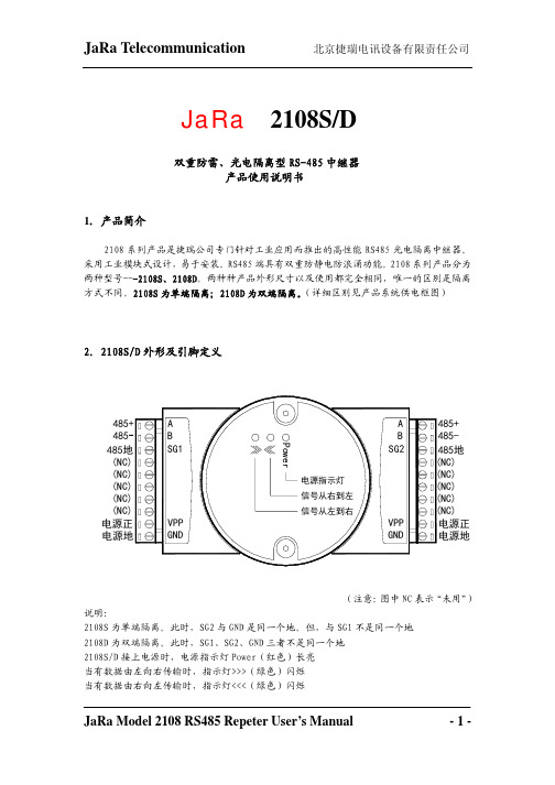
JaRa 2108S/D双重防雷、光电隔离型RS-485中继器产品使用说明书1.产品简介2108系列产品是捷瑞公司专门针对工业应用而推出的高性能RS485光电隔离中继器。
采用工业模块式设计,易于安装。
RS485端具有双重防静电防浪涌功能。
2108系列产品分为两种型号---2108S、2108D。
两种种产品外形尺寸以及使用都完全相同,唯一的区别是隔离方式不同。
2108S为单端隔离;2108D为双端隔离。
(详细区别见产品系统供电框图)2.2108S/D外形及引脚定义(注意:图中NC表示“未用”)说明:2108S为单端隔离。
此时,SG2与GND是同一个地。
但,与SG1不是同一个地2108D为双端隔离。
此时,SG1、SG2、GND三者不是同一个地2108S/D接上电源时,电源指示灯Power(红色)长亮当有数据由左向右传输时,指示灯>>>(绿色)闪烁当有数据由右向左传输时,指示灯<<<(绿色)闪烁3.性能参数接口标准 兼容EIA/TIA的RS485标准传输介质 普通双绞线传输距离 单端0---1.2Km,双端2400m,可使您的485网络再延长1200m通信速率 300---115200bps挂接点数 32个标准节点隔离电压 2500V供电方式 在接线柱的VPP和GND之间接+8VDC~+30VDC直流电源最大功率 <1W信号 SG1端:A、B、SG1(可选);SG2端:A、B、SG2(可选)工作方式 半双工通信协议 透明工作温度 -10℃---50℃相对湿度 5%---95%备注:2108S/D的外部供电电源设计为可以从两端提供,既,将+9VDC~+24VDC直流电源接在2108S/D的任何一端都可以。
两端的电源地(GND)是相通的,但两端的电源VPP是不通的。
详细情况参见2108S/D的内部供电框图4.2108S/D的内部电源供电框图4.1 2108S(单端隔离)(注意:2108S的SG1端485的信号地(SG1)与电源地(GND)是同一个地)4.2 2108D(双端隔离)(注意:2108D的右信号地SG1、信号地SG2与电源地(GND)彼此不是同一个地)5.应用举例5.1 2108S/D并联方式扩展RS-485网络说明:并联2108S/D方式用于在同一个区域内扩展您的485通信网络,增加您的485网络的设备数量。
ME2108最新资料(2015版)

Function Feed Back Output voltage monitor, IC internal power supply NC Ground External switch transistor drive
V10.0
3
ME2108ห้องสมุดไป่ตู้
Absolute Maximum Ratings PARAMETER VIN Input Voltage Lx Pin voltage EXT Pin voltage CE Pin voltage Lx Pin current EXT Pin current Vdd input voltage SOT23 Continuous Total Power Dissipation SOT89 TO92 Operating Ambient Temperature Storage Temperature Soldering temperature and time Block Diagram SYMBAL VIN VLX VEXT VCE ILX IEXT Vdd Pd Pd Pd TOpr Tstg Tsolder RATINGS 6.5 6.5 -0.3~Vout+0.3 -0.3~Vout+0.3 600 ±30 6.5 300 500 500 -25~+85 -40~+125 260℃, 10s UNITS V V V V mA mA V mW mW mW ℃ ℃
V10.0
5
ME2108
ME2108F SYMBOL VFB Vstart Vhold IDD1 IDD2 ILX ILXleak Fosc Maxdty EFFI VFB=3.3V , Fosc=180kHz PARAMETER Output Feedback Voltage Oscillation Start-up Voltage Oscillation Hold Voltage Supply Current 1 Supply Current 2 Lx Switching Current Lx Leakage Current Oscillation Frequency Duty Ratio Efficiency IOUT=1mA, VIN:0→2V IOUT=1mA, VIN:2→0V No external component Vout=Vout×0.95, Vout=Vout+0.5V VLX=0.4V, Vout=Vout×0.95 Vout=VLX=6V Vout=set Vout×0.95 on(VLX“L”)side 180 84 85 CONDITIONS MIN 3.22 TYP 3.3 0.8 0.45 80 10 360 0.5 MAX 3.38 0.9 UNITS V V V µA µA mA µA kHz % %
MAX809MTRG资料

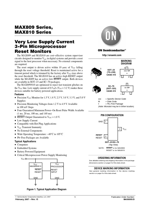
MAX809 Series,MAX810 SeriesVery Low Supply Current3−Pin MicroprocessorReset MonitorsThe MAX809 and MAX810 are cost−effective system supervisor circuits designed to monitor V CC in digital systems and provide a reset signal to the host processor when necessary. No external components are required.The reset output is driven active within 10 m sec of V CC falling through the reset voltage threshold. Reset is maintained active for a timeout period which is trimmed by the factory after V CC rises above the reset threshold. The MAX810 has an active−high RESET output while the MAX809 has an active−low RESET output. Both devices are available in SOT−23 and SC−70 packages.The MAX809/810 are optimized to reject fast transient glitches on the V CC line. Low supply current of 0.5 m A (V CC= 3.2 V) makes these devices suitable for battery powered applications.Features•Precision V CC Monitor for 1.5 V, 1.8 V, 2.5 V, 3.0 V, 3.3 V, and 5.0 V Supplies•Precision Monitoring V oltages from 1.2 V to 4.9 V Availablein 100 mV Steps•Four Guaranteed Minimum Power−On Reset Pulse Width Available (1 ms, 20 ms, 100 ms, and 140 ms)•RESET Output Guaranteed to V CC = 1.0 V.•Low Supply Current•Compatible with Hot Plug Applications•V CC Transient Immunity•No External Components•Wide Operating Temperature: −40°C to 105°C•Pb−Free Packages are AvailableTypical Applications•Computers•Embedded Systems•Battery Powered Equipment•Critical Microprocessor Power Supply MonitoringV CCFigure 1. Typical Application DiagramSee general marking information in the device marking section on page 8 of this data sheet.DEVICE MARKING INFORMATIONSee detailed ordering and shipping information in the package dimensions section on page 8 of this data sheet.ORDERING INFORMATIONPIN DESCRIPTIONPin No.Symbol Description1GND Ground2RESET (MAX809)RESET output remains low while V CC is below the reset voltage threshold, and for a reset timeoutperiod after V CC rises above reset threshold2RESET (MAX810)RESET output remains high while V CC is below the reset voltage threshold, and for a reset timeoutperiod after V CC rises above reset threshold3V CC Supply Voltage (Typ)ABSOLUTE MAXIMUM RATINGSRating Symbol Value Unit Power Supply Voltage (V CC to GND)V CC−0.3 to 6.0V RESET Output Voltage (CMOS)−0.3 to (V CC + 0.3)V Input Current, V CC20mA Output Current, RESET20mAdV/dt (V CC)100V/m secThermal Resistance, Junction−to−Air (Note 1)SOT−23SC−70R q JA301314°C/WOperating Junction Temperature Range T J−40 to +105°C Storage Temperature Range T stg−65 to +150°C Lead Temperature (Soldering, 10 Seconds)T sol+260°C ESD ProtectionHuman Body Model (HBM): Following Specification JESD22−A114 Machine Model (MM): Following Specification JESD22−A1152000200VLatchup Current Maximum Rating: Following Specification JESD78 Class IIPositiveNegative I Latchup200200mAStresses exceeding Maximum Ratings may damage the device. Maximum Ratings are stress ratings only. Functional operation above the Recommended Operating Conditions is not implied. Extended exposure to stresses above the Recommended Operating Conditions may affect device reliability.1.This based on a 35x35x1.6mm FR4 PCB with 10mm2 of 1 oz copper traces under natural convention conditions and a single componentcharacterization.2.The maximum package power dissipation limit must not be exceeded.P D+T J(max)*T Aq JAwith T J(max) = 150°CELECTRICAL CHARACTERISTICS T A = −40°C to +105°C unless otherwise noted. Typical values are at T A = +25°C. (Note 3) Characteristic Symbol Min Typ Max Unit V CC RangeT A = 0°C to +70°CT A = −40°C to +105°C 1.01.2−−5.55.5VSupply CurrentV CC = 3.3 VT A = −40°C to +85°CT A = 85°C to +105°C V CC = 5.5 VT A = −40°C to +85°CT A = 85°C to +105°C I CC−−−−0.5−0.8−1.22.01.82.5m AReset Threshold (V in Decreasing) (Note 4)V TH V MAX809SN490T A = +25°CT A = −40°C to +85°C T A = +85°C to +105°C 4.834.784.664.9−−4.975.025.14MAX8xxLTR, MAX8xxSQ463T A = +25°CT A = −40°C to +85°C T A = +85°C to +105°C 4.564.504.404.63−−4.704.754.86MAX809HTRT A = +25°CT A = −40°C to +85°C T A = +85°C to +105°C 4.484.434.324.55 4.624.674.78MAX8xxMTR, MAX8xxSQ438T A = +25°CT A = −40°C to +85°C T A = +85°C to +105°C 4.314.274.164.38 4.454.494.60MAX809JTR, MAX8xxSQ400T A = +25°CT A = −40°C to +85°C T A = +85°C to +105°C 3.943.903.804.00−−4.064.104.20MAX8xxTTR, MAX809SQ308T A = +25°CT A = −40°C to +85°C T A = +85°C to +105°C 3.043.002.923.08−−3.113.163.24MAX8xxSTR, MAX8xxSQ293T A = +25°CT A = −40°C to +85°C T A = +85°C to +105°C 2.892.852.782.93−−2.963.003.08MAX8xxRTR, MAX8xxSQ263T A = +25°CT A = −40°C to +85°C T A = +85°C to +105°C 2.592.562.492.63−−2.662.702.77MAX809SN232, MAX809SQ232T A = +25°CT A = −40°C to +85°C T A = +85°C to +105°C 2.282.252.212.32−−2.352.382.45MAX809SN160T A = +25°CT A = −40°C to +85°C T A = +85°C to +105°C 1.581.561.521.60−−1.621.641.68MAX809SN120, MAX8xxSQ120T A = +25°CT A = −40°C to +85°C T A = +85°C to +105°C 1.181.171.141.20−−1.221.231.263.Production testing done at T A = 25°C, over temperature limits guaranteed by design.4.Contact your ON Semiconductor sales representative for other threshold voltage options.ELECTRICAL CHARACTERISTICS(continued) T A = −40°C to +105°C unless otherwise noted. Typical values are atT A = +25°C. (Note 5)Characteristic Symbol Min Typ Max Unit Detector Voltage Threshold Temperature Coefficient−30−ppm/°C V CC to Reset Delay V CC = V TH to (V TH − 100 mV)−10−m secReset Active TimeOut Period (Note 6) MAX8xxSN(Q)293D1MAX8xxSN(Q)293D2MAX8xxSN(Q)293D3MAX8xxSN(Q)293t RP1.020100140−−−−3.366330460msecRESET Output Voltage Low (No Load) (MAX809)V CC = V TH − 0.2 V1.6 V v V TH v2.0 V, I SINK = 0.5 mA2.1 V v V TH v 4.0 V, I SINK = 1.2 mA4.1 V v V TH v 4.9 V, I SINK = 3.2 mAV OL−−0.3VRESET Output Voltage High (No Load) (MAX809)V CC = V TH + 0.2 V1.6 V v V TH v2.4 V, I SOURCE = 200 m A2.5 V v V TH v 4.9 V, I SOURCE = 500 m AV OH0.8 V CC−−VRESET Output Voltage High (No Load) (MAX810)V CC = V TH + 0.2 V1.6 V v V TH v2.4 V, I SOURCE = 200 m A2.5 V v V TH v 4.9 V, I SOURCE = 500 m AV OH0.8 V CC−−VRESET Output Voltage Low (No Load) (MAX810)V CC = V TH − 0.2 V1.6 V v V TH v2.0 V, I SINK = 0.5 mA2.1 V v V TH v 4.0 V, I SINK = 1.2 mA4.1 V v V TH v 4.9 V, I SINK = 3.2 mAV OL−−0.3V5.Production testing done at T A = 25°C, over temperature limits guaranteed by design.6.Contact your ON Semiconductor sales representative for timeout options availability for other threshold voltage options.TYPICAL OPERATING CHARACTERISTICS0.50.40.30.20.10S U P P L Y C U R R E N T (m A )0.60.250.150.0500.35S U P P L Y C U R R E N T (m A )−50−2502550TEMPERATURE (°C)S U P P L Y C U R R E N T (m A )75100−50−2502550TEMPERATURE (°C)100Figure 6. Supply Current vs. Temperature(No Load, MAX809)Figure 7. Supply Current vs. Temperature (NoLoad, MAX810)750.100.200.30TYPICAL OPERATING CHARACTERISTICS252015105.00−50−25255075TEMPERATURE (°C)O U T P U T V O L T A G E V C C (m V )30100250−50−252575125TEMPERATURE (°C)125P O W E R −D O W N R E S E T D E L A Y (m s e c )125−50−2502550TEMPERATURE (°C)N O R M A L I Z E D P O W E R −U P R E S E T T I M E O U T0.70.80.91.21.375100Figure 10. Power−Down Reset Delay vs.Temperature and Overdrive (V TH = 1.2 V)Figure 11. Power−Down Reset Delay vs.Temperature and Overdrive (V TH = 4.9 V)Figure 12. Normalized Power−Up Reset vs.Temperature10050751.01.110050APPLICATIONS INFORMATIONV CC Transient RejectionThe MAX809 provides accurate V CC monitoring and reset timing during power−up, power−down, and brownout/sag conditions, and rejects negative−going transients (glitches) on the power supply line. Figure 13shows the maximum transient duration vs. maximum negative excursion (overdrive) for glitch rejection. Any combination of duration and overdrive which lies under the curve will not generate a reset signal. Combinations above the curve are detected as a brownout or power−down.Typically, transient that goes 100 mV below the reset threshold and lasts 5.0 m s or less will not cause a reset pulse.Transient immunity can be improved by adding a capacitor in close proximity to the V CC pin of the MAX809.Figure 13. Maximum Transient Duration vs.Overdrive for Glitch Rejection at 25°CV CC1011060M A X I M U M T R A N S I E N T D U R A T I O N (m s e c )RESET COMPARATOR OVERDRIVE (mV)410160210260310360RESET Signal Integrity During Power−DownThe MAX809 RESET output is valid to V CC = 1.0 V .Below this voltage the output becomes an “open circuit” and does not sink current. This means CMOS logic inputs to the Microprocessor will be floating at an undetermined voltage.Most digital systems are completely shutdown well above this voltage. However, in situations where RESET must bemaintained valid to V CC = 0 V , a pull−down resistor must be connected from RESET to ground to discharge stray capacitances and hold the output low (Figure 14). This resistor value, though not critical, should be chosen such that it does not appreciably load RESET under normal operation (100 k W will be suitable for most applications).Figure 14. Ensuring RESET Valid to V CC = 0 VProcessors With Bidirectional I/O PinsSome Microprocessor’s have bidirectional reset pins.Depending on the current drive capability of the processor pin, an indeterminate logic level may result if there is a logic conflict. This can be avoided by adding a 4.7 k W resistor in series with the output of the MAX809 (Figure 15). If there are other components in the system which require a reset signal, they should be buffered so as not to load the reset line.If the other components are required to follow the reset I/O of the Microprocessor, the buffer should be connected as shown with the solid line.Figure 15. Interfacing to Bidirectional Reset I/OBUFFERED RESETORDERING, MARKING AND THRESHOLD INFORMATIONPart Number V TH*(V)Timeout*(ms)Description Marking Package Shipping†MAX809SN160T1 1.60140−460Push−Pull RESET SAA SOT23−33000 / Tape & ReelMAX809SN160T1G 1.60140−460SAA SOT23−3(Pb−Free)MAX809SN232T1 2.32140−460SQP SOT23−3MAX809SN232T1G 2.32140−460SQP SOT23−3(Pb−Free)MAX809RTR 2.63140−460SPS SOT23−3MAX809RTRG 2.63140−460SPS SOT23−3(Pb−Free)MAX809STR 2.93140−460SPT SOT23−3MAX809STRG 2.93140−460SPT SOT23−3(Pb−Free)MAX809TTR 3.08140−460SPU SOT23−3MAX809TTRG 3.08140−460SPU SOT23−3(Pb−Free)MAX809JTR 4.00140−460SPR SOT23−3MAX809JTRG 4.00140−460SPR SOT23−3(Pb−Free)MAX809MTR 4.38140−460SPV SOT23−3MAX809MTRG 4.38140−460SPV SOT23−3(Pb−Free)MAX809HTR 4.55140−460SBD SOT23−3MAX809HTRG 4.55140−460SBD SOT23−3(Pb−Free)MAX809LTR 4.63140−460SPW SOT23−3MAX809LTRG 4.63140−460SPW SOT23−3(Pb−Free)MAX809SN490T1 4.90140−460SBH SOT23−3MAX809SN490T1G 4.90140−460SBH SOT23−3(Pb−Free)MAX809SN120T1G 1.20140−460SSO SOT23−3(Pb−Free)MAX809SN293D1T1G 2.931−3.3SSP SOT23−3(Pb−Free)MAX809SN293D2T1G 2.9320−66SSQ SOT23−3(Pb−Free)MAX809SN293D3T1G 2.93100−330SSR SOT23−3(Pb−Free)MAX809SQ120T1G 1.20140−460ZD SC70−3(Pb−Free)MAX809SQ232T1G 2.32140−460ZE SC70−3(Pb−Free)MAX809SQ263T1G 2.63140−460ZF SC70−3(Pb−Free)MAX809SQ293T1G 2.93140−460ZG SC70−3(Pb−Free)MAX809SQ308T1G 3.08140−460ZH SC70−3(Pb−Free)MAX809SQ400T1G 4.00140−460SZ SC70−3(Pb−Free)MAX809SQ438T1G 4.38140−460ZI SC70−3(Pb−Free)MAX809SQ463T1G 4.63140−460ZJ SC70−3(Pb−Free)MAX809SQ293D1T1G 2.931−3.3ZK SC70−3(Pb−Free)MAX809SQ293D2T1G 2.9320−66ZL SC70−3(Pb−Free)MAX809SQ293D3T1G 2.93100−330ZM SC70−3(Pb−Free)†For information on tape and reel specifications,including part orientation and tape sizes, please refer to our Tape and Reel Packaging Specifications Brochure, BRD8011/D.*Contact your ON Semiconductor sales representative for other threshold voltage options.ORDERING, MARKING AND THRESHOLD INFORMATIONPart Number V TH*(V)Timeout*(ms)Description Marking Package Shipping†MAX810RTR 2.63140−460Push−Pull RESET SPX SOT23−33000 / Tape & ReelMAX810RTRG 2.63140−460SPX SOT23−3(Pb−Free)MAX810STR 2.93140−460SPY SOT23−3MAX810STRG 2.93140−460SPY SOT23−3(Pb−Free)MAX810TTR 3.08140−460SPZ SOT23−3MAX810TTRG 3.08140−460SPZ SOT23−3(Pb−Free)MAX810MTR 4.38140−460SQA SOT23−3MAX810MTRG 4.38140−460SQA SOT23−3(Pb−Free)MAX810LTR 4.63140−460SQB SOT23−3MAX810LTRG 4.63140−460SQB SOT23−3(Pb−Free)MAX810SN120T1G 1.20140−460SSS SOT23−3(Pb−Free)MAX810SN293D1T1G 2.931−3.3SST SOT23−3(Pb−Free)MAX810SN293D2T1G 2.9320−66SSU SOT23−3(Pb−Free)MAX810SN293D3T1G 2.93100−330SSZ SOT23−3(Pb−Free)MAX810SQ120T1G 1.20140−460ZN SC70−3(Pb−Free)MAX810SQ263T1G 2.63140−460ZO SC70−3(Pb−Free)MAX810SQ293T1G 2.93140−460ZP SC70−3(Pb−Free)MAX810SQ438T1G 4.38140−460ZQ SC70−3(Pb−Free)MAX810SQ463T1G 4.63140−460ZR SC70−3(Pb−Free)MAX810SQ293D1T1G 2.931−3.3ZS SC70−3(Pb−Free)MAX810SQ293D2T1G 2.9320−66ZT SC70−3(Pb−Free)MAX810SQ293D3T1G 2.93100−330ZU SC70−3(Pb−Free)†For information on tape and reel specifications,including part orientation and tape sizes, please refer to our Tape and Reel Packaging Specifications Brochure, BRD8011/D.*Contact your ON Semiconductor sales representative for other threshold voltage options.PACKAGE DIMENSIONSSOT−23 (TO236)CASE 318−08ISSUE AN*For additional information on our Pb−Free strategy and solderingdetails, please download the ON Semiconductor Soldering and Mounting Techniques Reference Manual, SOLDERRM/D.SOLDERING FOOTPRINT*ǒmm inchesǓSCALE 10:1NOTES:1.DIMENSIONING AND TOLERANCING PER ANSI Y14.5M, 1982.2.CONTROLLING DIMENSION: INCH.3.MAXIMUM LEAD THICKNESS INCLUDES LEAD FINISH THICKNESS. MINIMUM LEADTHICKNESS IS THE MINIMUM THICKNESS OF BASE MATERIAL.4.318−01 THRU −07 AND −09 OBSOLETE, NEW STANDARD 318−08.VIEW CDIM A MIN NOM MAX MINMILLIMETERS0.89 1.00 1.110.035INCHES A10.010.060.100.001b 0.370.440.500.015c 0.090.130.180.003D 2.80 2.90 3.040.110E 1.20 1.30 1.400.047e 1.78 1.90 2.040.070L 0.100.200.300.0040.0400.0440.0020.0040.0180.0200.0050.0070.1140.1200.0510.0550.0750.0810.0080.012NOM MAX L1 2.102.40 2.640.0830.0940.104H E0.350.540.690.0140.0210.029MAX809 Series, MAX810 SeriesPACKAGE DIMENSIONSSC−70 (SOT−323)CASE 419−04ISSUE Mǒmm inchesǓSCALE 10:1*For additional information on our Pb−Free strategy and solderingdetails, please download the ON Semiconductor Soldering and Mounting Techniques Reference Manual, SOLDERRM/D.ON Semiconductor and are registered trademarks of Semiconductor Components Industries, LLC (SCILLC). SCILLC reserves the right to make changes without further notice to any products herein. SCILLC makes no warranty, representation or guarantee regarding the suitability of its products for any particular purpose, nor does SCILLC assume any liability arising out of the application or use of any product or circuit, and specifically disclaims any and all liability, including without limitation special, consequential or incidental damages.“Typical” parameters which may be provided in SCILLC data sheets and/or specifications can and do vary in different applications and actual performance may vary over time. All operating parameters, including “Typicals” must be validated for each customer application by customer’s technical experts. SCILLC does not convey any license under its patent rights nor the rights of others. SCILLC products are not designed, intended, or authorized for use as components in systems intended for surgical implant into the body, or other applications intended to support or sustain life, or for any other application in which the failure of the SCILLC product could create a situation where personal injury or death may occur. Should Buyer purchase or use SCILLC products for any such unintended or unauthorized application, Buyer shall indemnify and hold SCILLC and its officers, employees, subsidiaries, affiliates,and distributors harmless against all claims, costs, damages, and expenses, and reasonable attorney fees arising out of, directly or indirectly, any claim of personal injury or death associated with such unintended or unauthorized use, even if such claim alleges that SCILLC was negligent regarding the design or manufacture of the part. SCILLC is an Equal Opportunity/Affirmative Action Employer. This literature is subject to all applicable copyright laws and is not for resale in any manner.PUBLICATION ORDERING INFORMATION元器件交易网。
MEMORY存储芯片MAX208CWG+T中文规格书

Detailed Description The MAX200–MAX209/MAX211/MAX213 consist of three sections: charge-pump voltage converters, drivers (trans-mitters), and receivers. Each section is described in detail.+5V to ±10V Dual Charge-Pump Voltage Converter The +5V to ±10V conversion is performed by two charge-pump voltage converters (Figure 4). The first uses capaci-tor C1 to double +5V to +10V, storing +10V on the V+output filter capacitor, C3. The second chargepump volt-age converter uses capacitor C2 to invert +10V to -10V,storing -10V on the V- output filter capacitor, C4.The MAX201 and MAX209 include only the V+ to Vcharge pump, and are intended for applications that have a V CC = +5V supply and a V+ supply in the +9V to +13.2V range.In shutdown mode, V+ is internally connected to V CC by a 1kΩ pulldown resistor and V- is internally connected to ground by a 1kΩ pullup resistor.RS-232 Drivers When V CC = +5V, the typical driver output-voltage swing is ±8V when loaded with a nominal 5kΩ RS-232 receiver. The output swing is guaranteed to meet the EIA/TIA-232E and V.28 specifications, which call for ±5V minimum out-put levels under worst-case conditions. These include a minimum 3kΩ load, V CC = +4.5V, and the maximum operating temperature. The open-circuit output-voltage swing ranges from (V+ - 0.6V) to V-.Input thresholds are both CMOS and TTL compatible. The inputs of unused drivers can be left unconnected since 400kΩ pullup resistors to V CC are included onchip. Since all drivers invert, the pullup resistors force the outputs of unused drivers low. The input pullup resistors typically source 15μA; therefore, the driver inputs should be driven high or open circuited to minimize power-supply current in shutdown mode.When in low-power shutdown mode, the driver outputs are turned off and their leakage current is less than 1mA, even if the transmitter output is backdriven between 0V and (V CC + 6V). Below -0.5V, the transmitter output is diode clamped to ground with a 1kΩ series impedance. The transmitter output is also zener clamped to approxi-mately (V CC + 6V), with a 1kΩ series impedance.Figure 1. Shutdown Current Test CircuitFigure 2. Receiver Output Enable and Disable Timing Integrated │ 5找MEMORY 、二三极管上美光存储Applications InformationCapacitor SelectionThe type of capacitor used is not critical for properoperation. Ceramic capacitors are suggested. To ensureproper RS-232 signal levels over temperature whenusing 0.1µF capacitors, make sure the capacitance valuedoes not degrade excessively as the temperature varies.If in doubt, use capacitors with a larger nominal value.Also observe the capacitors’ ESR value over tempera-ture, since it influences the amount of ripple on V+ andV-. To reduce the output impedance at V+ and V-, uselarger capacitors (up to 10µF). If polarized capacitors areused, obey the polarities shown in Figure 1 and the pinconfigurations.Driving Multiple ReceiversEach transmitter is designed to drive a single receiver.Transmitters can be paralleled to drive multiple receivers.Driver Outputs When Exiting Shutdown Figure 5 shows two driver outputs exiting shutdown. As they become active, the two driver outputs go to opposite RS-232 levels (one driver input is high, the other is low). Each driver is loaded with 3kΩ in parallel with 2500pF. The driver outputs display no ringing or undesirable tran-sients as they come out of shutdown.Power-Supply Decoupling In applications that are sensitive to power-supply noise, decouple V CC to ground with a capacitor of the same value as the charge-pump capacitors.V+ and V- as Power Supplies A small amount of power can be drawn from V+ and V-,although this reduces noise margins.Power Supplies for MAX201/MAX209If at power-up the V+ supply rises after the V CC supply,place a diode (e.g., 1N914) in series with the V+ supply.Table 2. Summary of EIA/TIA-232E, V.28 SpecificationsTable 3. DB9 Cable Connections Commonly Used for EIA/TIA-232E and V.24 Asynchronous InterfacesPARAMETERCONDITION EIA/TIA-232E, V.28 SPECIFICATION Driver Output Voltage: 0 Level3kΩ to 7kΩ load +5.0V to +15V Driver Output Voltage: 1 Level3kΩ to 7kΩ load -5.0V to -15V Output Level, MaximumNo load ±25V Data Rate3kΩ ≤ R L ≤ 7kΩ, C L ≤ 2500pF Up to 20kbps Receiver Input Voltage: 0 Level—+3.0V to +15V Receiver Input Voltage: 1 Level—-3.0V to -15V Input Level, Maximum—±25V Instantaneous Slew Rate, Maximum3kΩ ≤ R L ≤ 7kΩ, C L ≤ 2500pF 30V/µs Driver Output Short-Circuit Current, Maximum—100mA Transition Rate on Driver OutputV.281ms or 3% of the period EIA/TIA-232E 4% of the period Driver Output Resistance -2V < V OUT < +2V 300ΩPINNAME CONNECTION 1Received Line Signal Detector, sometimes called Carrier Detect (DCD)Handshake from DCE 2Receive Data (RD)Data from DCE 3Transmit Data (TD)Data from DTE 4Data Terminal Ready Handshake from DTE 5Signal Ground Reference point for signals 6Data Set Ready (DSR)Handshake from DCE 7Request to Send (RTS)Handshake from DTE 8Clear to Send (CTS)Handshake from DCE 9Ring Indicator Handshake from DCEMAX200–MAX209/MAX211/MAX213+5V, RS-232 Transceivers with 0.1μF External Capacitors Integrated │ 8。
MAX809STRG中文资料
(1 ms, 20 ms, 100 ms, and 140 ms)
• RESET Output Guaranteed to VCC = 1.0 V. • Low Supply Current • Compatible with Hot Plug Applications • VCC Transient Immunity • No External Components • Wide Operating Temperature: −40°C to 105°C • Pb−Free Packages are Available
characterization.
2. The maximum package power dissipation limit must not be exceeded.
PD
+
TJ(max) * RqJA
TA
with TJ(max) = 150°C
2
元器件交易网
4.78
−
5.02
4.66
−
5.14
MAX8xxLTR, MAX8xxSQ463 TA = +25°C TA = −40°C to +85°C TA = +85°C to +105°C
4.56
4.63
4.70
4.50
−
4.75
4.40
−
4.86
MAX809HTR TA = +25°C TA = −40°C to +85°C TA = +85°C to +105°C
CP2108

Virtual COM Port Drivers
Works
with existing COM port PC applications distribution license Windows 8/7/Vista/XP/Server 2003 Mac OS X Linux
Royalty-free
of 16 GPIO pins with configurable options pin support Usable as inputs, open-drain or push-pull outputs 4 configurable clock outputs for external devices RS-485 bus transceiver control Toggle LED upon transmission Toggle LED upon reception
6
DSR(0-3) RTS(0-3)
UART1
CTS(0-3) RX(0-3) TX(0-3)
Data FIFO
UARTn (0-3)
VIO
UART2
GPIO.0 – GPIO.15
18 EEPROM (Product Customization)
RESET
SUSPEND
UART3
/SUSPEND
(3.0 V to VDD) (2.7 to 6.0 V)
independent UART interfaces Integrated USB transceiver; no external resistor required Integrated clock; no external crystal required Integrated programmable EEPROM for storing customizable product information On-chip power-on reset circuit On-chip voltage regulator: 3.3 V output
ADG2108资料

I 2C ® CMOS 8 × 10 Unbuffered Analog Switch Array with Dual/Single SuppliesADG2108Rev. 0Information furnished by Analog Devices is believed to be accurate and reliable. However , no responsibility is assumed by Analog Devices for its use, nor for any infringements of patents or other rights of third parties that may result from its use. Specifications subject to change without notice. No license is granted by implication or otherwise under any patent or patent rights of Analog Devices. T rademarks and registered trademarks are the property of their respective owners.One Technology Way, P.O. Box 9106, Norwood, M A 02062-9106, U.S.A.Tel: 781.329.4700 Fax: 781.461.3113 ©2006 Analog Devices, Inc. All rights reserved.FEATURESI 2C-compatible interface3.4 MHz high speed I 2C option 32-lead LFCSP_VQ (5 mm × 5 mm) Double-buffered input logicSimultaneous update of multiple switches Up to 300 MHz bandwidthFully specified at dual ±5 V/single +12 V operation On resistance 35 Ω maximum Low quiescent current < 20 μAAPPLICATIONSAV switching in TVAutomotive infotainment AV receivers CCTVUltrasound applications KVM switchingTelecom applicationsTest equipment/instrumentation PBX systemsGENERAL DESCRIPTIONThe ADG2108 is an analog cross point switch with an array size of 8 × 10. The switch array is arranged so that there are eight columns by 10 rows, for a total of 80 switch channels. The array is bidirectional, and the rows and columns can be configured as either inputs or outputs. Each of the 80 switches can be addressed and configured through the I 2C-compatible interface. Standard, full speed, and high speed (3.4 MHz) I 2C interfaces are supported. Any simultaneous switch combination is allowed. An additional feature of the ADG2108 is that switches can be updated simultaneously, using the LDSW command. In addition, a RESET option allows all of the switch channels to be reset/off. At power on, all switches are in the off condition. The device is packaged in a 32-lead, 5 mm × 5 mm LFCSP_VQ.FUNCTIONAL BLOCK DIAGRAMV V V SCL SDA05898-001Figure 1.ADG2108Rev. 0 | Page 2 of 28TABLE OF CONTENTSFeatures..............................................................................................1 Applications.......................................................................................1 General Description.........................................................................1 Functional Block Diagram..............................................................1 Revision History...............................................................................2 Specifications.....................................................................................3 I 2C Timing Specifications............................................................7 Timing Diagram...........................................................................8 Absolute Maximum Ratings............................................................9 ESD Caution..................................................................................9 Pin Configuration and Function Descriptions...........................10 Typical Performance Characteristics...........................................11 Test Circuits.....................................................................................15 Terminology....................................................................................17 Theory of Operation......................................................................18 RESET /Power-On Reset............................................................18 Load Switch (LDSW).................................................................18 Readback.....................................................................................18 Serial Interface................................................................................19 High Speed I 2C Interface...........................................................19 Serial Bus Address......................................................................19 Writing to the ADG2108...............................................................20 Input Shift Register....................................................................20 Write Operation..........................................................................22 Read Operation...........................................................................22 Evaluation Board............................................................................24 Using the ADG2108 Evaluation Board...................................24 Power Supply...............................................................................24 Schematics...................................................................................25 Outline Dimensions.......................................................................27 Ordering Guide.. (27)REVISION HISTORY4/06—Revision 0: Initial VersionADG2108SPECIFICATIONSV DD = 12 V ± 10%, V SS = 0 V, V L = 5 V, GND = 0 V, all specifications T MIN to T MAX, unless otherwise noted.1Rev. 0 | Page 3 of 28ADG2108Rev. 0 | Page 4 of 28B Version Y VersionParameter +25°C −40°C to +85°C +25°C −40°C to+125°CUnit Conditions LOGIC INPUTS (SCL, SDA)2 Input High Voltage, V INH 0.7 V L 0.7 V L V min V L + 0.3 V L + 0.3 V max Input Low Voltage, V INL −0.3 −0.3 V min 0.3 V L 0.3 V L V max Input Leakage Current, I IN 0.005 0.005 μA typ V IN = 0 V to V L ±1 ±1 μA max Input Hysteresis 0.05 V L 0.05 V L V min Input Capacitance, C IN 7 7 pF typLOGIC OUTPUT (SDA)2Output Low Voltage, V OL 0.4 0.4 V max ISINK = 3 mA 0.6 0.6 V max I SINK = 6 mA Floating State Leakage Current ±1 ±1 μA max POWER REQUIREMENTS I DD 0.05 0.05 μA typ Digital inputs = 0 V or V L 1 1 μA max I SS 0.05 0.05 μA typ Digital inputs = 0 V or V L 1 1 μA max I L Digital inputs = 0 V or V LInterface Inactive 0.3 0.3 μA typ2 2 μA max Interface Active: 400 kHz f SCL 0.1 0.1 mA typ 0.2 0.2 mA max Interface Active: 3.4 MHz f SCL 0.4 0.4 mA typ -HS model only 1.2 1.7 mA max1 Temperature range is as follows: B version: −40°C to +85°C; Y version: −40°C to +125°C. 2Guaranteed by design, not subject to production test.ADG2108 V DD = +5 V ± 10%, V SS = −5 V ± 10%, V L = 5 V, GND = 0 V, all specifications T MIN to T MAX, unless otherwise noted.1Rev. 0 | Page 5 of 28ADG2108Rev. 0 | Page 6 of 28B Version Y VersionParameter +25°C −40°C to +125°C +25°C −40°C to +125°C Unit ConditionsInput Leakage Current, I IN 0.005 0.005 μA typ V IN = 0 V to V L ±1 ±1 μA max Input Hysteresis 0.05 V L 0.05 V L V min Input Capacitance, C IN 7 7 pF typLOGIC OUTPUT (SDA)2Output Low Voltage, V OL 0.4 0.4 V max ISINK = 3 mA 0.6 0.6 V max ISINK = 6 mA Floating State Leakage Current ±1 ±1 μA max POWER REQUIREMENTS I DD 0.05 0.005 μA typ Digital inputs = 0 V or V L 1 1 μA max I SS 0.05 0.005 μA typ Digital inputs = 0 V or V L 1 1 μA max I L Digital inputs = 0 V or V L Interface Inactive 0.3 0.3 μA typ 2 2 μA max Interface Active: 400 kHz f SCL 0.1 0.1 mA typ 0.1 0.1 mA max Interface Active: 3.4 MHz f SCL 0.4 0.4 mA typ -HS model only 0.3 0.3 mA max1 Temperature range is as follows: B version: –40°C to +85°C; Y version: –40°C to +125°C. 2Guaranteed by design, not subject to production test.ADG2108Rev. 0 | Page 7 of 28I 2C TIMING SPECIFICATIONSV DD = 5 V to 12 V; V SS = −5 V to 0 V; V L = 5 V; GND = 0 V; T A = T MIN to T MAX , unless otherwise noted (see Figure 2). Table 3.ADG2108 Limit at T MIN , T MAX Parameter 1Conditions M in M ax Unit Description f SCL Standard mode 100 kHz Serial clock frequency Fast mode 400 kHzHigh speed mode 2C B = 100 pF maximum 3.4 MHz C B = 400 pF maximum 1.7 MHz t 1 Standard mode 4 μs t HIGH , SCL high time Fast mode 0.6 μsHigh speed mode 2C B = 100 pF maximum 60 ns C B = 400 pF maximum 120 ns t 2 Standard mode 4.7 μs t LOW , SCL low time Fast mode 1.3 μsHigh speed mode 2C B = 100 pF maximum 160 ns C B = 400 pF maximum 320 ns t 3 Standard mode 250 ns t SU;DAT , data setup time Fast mode 100 nsHigh speed mode 210 ns t 43 Standard mode 0 3.45 μs t HD;DAT , data hold time Fast mode 0 0.9 μsHigh speed mode 2C B = 100 pF maximum 0 70 nsC B = 400 pF maximum 0 150 nst 5 Standard mode 4.7 μs t SU;STA , setup time for a repeated start condition Fast mode 0.6 μsHigh speed mode 2160 ns t 6 Standard mode 4 μs t HD;STA , hold time for a repeated start condition Fast mode 0.6 μs High speed mode 2160 ns t 7 Standard mode 4.7 μs t BUF , bus free time between a stop and a start condition Fast mode 1.3 μs t 8 Standard mode 4 μs t SU;STO , setup time for a stop condition Fast mode 0.6 μsHigh speed mode 2160 ns t 9 Standard mode 1000 ns t RDA , rise time of SDA signal Fast mode 20 + 0.1 C B 300 nsHigh speed mode 2C B = 100 pF maximum 10 80 ns C B = 400 pF maximum 20 160 ns t 10 Standard mode 300 ns t FDA , fall time of SDA signal Fast mode 20 + 0.1 C B 300 nsHigh speed mode 2C B = 100 pF maximum 10 80 ns C B = 400 pF maximum 20 160 nsADG2108Rev. 0 | Page 8 of 28ADG2108 Limit at T MIN , T MAX Parameter 1Conditionsin ax Unit Description t 11 Standard mode 1000 ns t RCL , rise time of SCL signal Fast mode 20 + 0.1 C B 300 nsHigh speed mode 2C B = 100 pF maximum 10 40 ns C B = 400 pF maximum 20 80 ns t 11A Standard mode 1000 ns t RCL1, rise time of SCL signal after a repeated start Fast mode 20 + 0.1 C B 300 ns condition and after an acknowledge bitHigh speed mode 2C B = 100 pF maximum 10 80 ns C B = 400 pF maximum 20 160 ns t 12 Standard mode 300 ns t FCL , fall time of SCL signal Fast mode 20 + 0.1 C B 300 nsHigh speed mode 2C B = 100 pF maximum 10 40 ns C B = 400 pF maximum 20 80 ns t SP Fast mode 0 50 ns Pulse width of suppressed spikeHigh speed mode 20 10 ns1Guaranteed by initial characterization. All values measured with input filtering enabled. C B refers to capacitive load on the bus line; t R and t F are measured between0.3 V DD and 0.7 V DD . 2High speed I 2C is available only in -HS models. 3A device must provide a data hold time for SDA to bridge the undefined region of the SCL falling edge.TIMING DIAGRAMS = START CONDITION P = STOP CONDITION05898-002Figure 2. Timing Diagram for 2-Wire Serial InterfaceADG2108Rev. 0 | Page 9 of 28ABSOLUTE MAXIMUM RATINGST A = 25°C, unless otherwise noted. Table 4.Parameter Rating V DD to V SS 15 V V DD to GND −0.3 V to +15 V V SS to GND +0.3 V to −7 V V L to GND −0.3 V to +7 V Analog Inputs V SS − 0.3 V to V DD + 0.3 V Digital Inputs −0.3 V to V L + 0.3 V or 30 mA,whichever occurs firstContinuous Current10 V on Input; Single InputConnected to Single Output65 mA 1 V on Input; Single InputConnected to Single Output90 mA 10 V on Input; Eight InputsConnected to Eight Outputs 25 mA Operating Temperature Range Industrial (B Version) –40°C to +85°C Automotive (Y Version) –40°C to +125°C Storage Temperature Range –65°C to +150°C Junction Temperature 150°C 32-Lead LFCSP_VQ θJA Thermal Impedance 108.2°C/W Reflow Soldering (Pb Free) Peak Temperature 260°C (+0/–5)Time at Peak Temperature 10 sec to 40 secStresses above those listed under Absolute Maximum Ratings may cause permanent damage to the device. This is a stress rating only; functional operation of the device at these or any other conditions above those indicated in the operationalsection of this specification is not implied. Exposure to absolute maximum rating conditions for extended periods may affect device reliability.ESD CAUTIONESD (electrostatic discharge) sensitive device. Electrostatic charges as high as 4000 V readily accumulate on the human body and test equipment and can discharge without detection. Although this product features proprietary ESD protection circuitry, permanent damage may occur on devices subjected to high energy electrostatic discharges. Therefore, proper ESD precautions are recommended to avoid performance degradation or loss of functionality.ADG2108Rev. 0 | Page 10 of 28PIN CONFIGURATION AND FUNCTION DESCRIPTIONSNC = NO CONNECTY 2Y 4Y 3Y 6Y 7Y 1Y 0Y 5NC V DD X9X8X7X6X5X4X1NC NC NC X3X2X0V SS R E S E TA 1S C LA 2A 0S D AG N DV L05898-003Exposed Paddle Soldered to V SSFigure 3. Pin Configuration11It is recommended that the exposed paddle be soldered to V SS to improve heat dissipation and crosstalk.TYPICAL PERFORMANCE CHARACTERISTICS200–512SOURCE VOLTAGE (V)R O N (Ω)18016014012010080604020–4–3–2–10123456789101105898-007Figure 4. Signal Range85756555453525–5.5 1.50.5–0.5–1.5–2.5–3.5–4.5SOURCE VOLTAGE (V)R O N (Ω)05898-017Figure 5. R ON vs. Source Voltage, Dual ±5 V SuppliesSOURCE VOLTAGE (V)R O N (Ω)05898-018Figure 6. R ON vs. Supplies, VDD = 12 V ± 10% 90807060504030SOURCE VOLTAGE (V)R O N (Ω)05898-025Figure 7. R ON vs. Source Voltage, V DD= 8 V ± 10%80706050403020100–510–1–2–3–4SOURCE VOLTAGE (V)R O N (Ω)05898-026Figure 8. R ONvs. Temperature, Dual ±5 V Supplies6050403020100654321SOURCE VOLTAGE (V)R O N (Ω)05898-027Figure 9. R ON vs. Temperature, V DD = 12 V8070605040302010000.5 1.0 1.5 2.0 2.5 3.0 3.5 4.0SOURCE VOLTAGE (V)R O N (Ω)05898-013Figure 10. R ON vs. Temperature, V DD = 8 V1614121086420020406080100120TEMPERATURE (°C)L E A K A G E C U R R E N T S (n A )05898-014Figure 11. On Leakage vs. Temperature, Dual ±5 V Supplies121086420–2020406080100120TEMPERATURE (°C)L E A K A G E C U R R E N T S (nA )05898-015Figure 12. Off Leakage vs. Temperature, Dual ±5 V Supplies 18121614108642–2020406080100120TEMPERATURE (°C)L E A K A G E C U R R E N T S (n A)05898-011Figure 13. On Leakage vs. Temperature, 12 V Single Supply9687543210–1020406080100120TEMPERATURE (°C)L E A K A G E C U R R E N T S (n A )05898-012Figure 14. Off Leakage vs. Temperature, 12 V Single Supply0–5.0SUPPLY VOLTAGE (V)C H A R G E I N J E C T I O N (p C )–0.5–1.0–1.5–2.0–2.5–3.0–3.5–4.0–4.5–3–5–1135791105898-030Figure 15. Charge Injection vs. Supply VoltageTEMPERATURE (°C)t O N /t O F F (n s )100120140160180200220240–40–2002040608010012005898-029Figure 16. t ON /t OFF Times vs. Temperature–2–8–7–6–5–4–3101G10G10M100k1kFREQUENCY (Hz)I N S E R T I O N L O SS (d B )05898-020Figure 17. Individual Inputs to Individual Outputs Bandwidth,Dual ±5 V Supply–1–2–8–7–6–5–4–3101G10G10M100k1kFREQUENCY (Hz)I N S E R T I O N LO S S (d B )05898-021Figure 18. Individual Inputs to Individual Outputs Bandwidth,12 V Single Supply–1–2–8–7–6–5–4–3FREQUENCY (Hz)I N S E R T I O N L O S S (dB )101G10G10M100k1k05898-022Figure 19. One Input to Eight Outputs Bandwidth, ±5 V Dual Supply–10–110–100–90–80–70–60–50–40–30–20101G10M100k1kFREQUENCY (Hz)I N S E R T I O N L O SS (d B )05898-023Figure 20. Off Isolation vs. Frequency–120–100–80–60–40–20101G10M 100k1k FREQUENCY (Hz)I N S E R T I O N L O S S (d B)05898-024Figure 21. Crosstalk vs. Frequency0.350.050.300.250.200.150.1000.5 1.0 1.5 2.0 2.5 3.0FREQUENCY (MHz)I L (m A )05898-016Figure 22. Digital Current (I L ) vs. Frequency0654321V LOGIC (V)I L (m A )05898-019Figure 23. Digital Current (I L ) vs. V LOGIC for Varying Digital Supply Voltage–1201001GFREQUENCY (Hz)A C P S R R (dB )–20–40–60–80–1001k 10k 100k 1M 10M 100M 05898-028Figure 24. ACPSRRTEST CIRCUITSThe test circuits show measurements on one channel for clarity, but the circuit applies to any of the switches in the matrix.V 05898-031Figure 25. On ResistanceV X 05898-032Figure 26. Off LeakageV Y05898-033Figure 27. On LeakageV XVV V AND t ON05898-034Figure 28. Switching Times, t ON , t OFFV V V OUT05898-035Figure 29. Charge InjectionV SV OUT OFF ISOLATION = 20 logVV 05898-036Figure 30. Off Isolation V OUT WITHOUT SWITCHV OUT WITH SWITCH INSERTION LOSS = 20 logV V 05898-037Figure 31. BandwidthV OUTΩCHANNEL-TO-CHANNEL CROSSTALK = 20 logV SV V 05898-038Figure 32. Channel-to-Channel CrosstalkTERMINOLOGYOn Resistance (R ON)The series on-channel resistance measured between theX input/output and the Y input/output.On Resistance Match (ΔR ON)The channel-to-channel matching of on resistance when channels are operated under identical conditions.On Resistance Flatness (R FLAT(ON))The variation of on resistance over the specified range produced by the specified analog input voltage change with a constant load current.Channel Off Leakage (I OFF)The sum of leakage currents into or out of an off channel input. Channel On Leakage (I ON)The current loss/gain through an on-channel resistance, creating a voltage offset across the device.Input Leakage Current (I IN)The current flowing into a digital input when a specified low level or high level voltage is applied to that input.Input Off Capacitance (C OFF)The capacitance between an analog input and ground when the switch channel is off.Input/Output On Capacitance (C ON)The capacitance between the inputs or outputs and ground when the switch channel is on.Digital Input Capacitance (C IN)The capacitance between a digital input and ground.Output On Switching Time (t ON)The time required for the switch channel to close. The time is measured from 50% of the logic input change to the time the output reaches 10% of the final value.Output Off Switching Time (t OFF)The time required for the switch to open. This time is measured from 50% of the logic input change to the time the output reaches 90% of the switch off condition. Total Harmonic Distortion + Noise (THD + N)The ratio of the harmonic amplitudes plus noise of a signal to the fundamental.−3 dB BandwidthThe frequency at which the output is attenuated by 3 dB.Off IsolationThe measure of unwanted signal coupling through an off switch. CrosstalkThe measure of unwanted signal that is coupled through from one channel to another as a result of parasitic capacitance. Differential GainThe measure of how much color saturation shift occurs when the luminance level changes. Both attenuation and amplification can occur; therefore, the largest amplitude change between any two levels is specified and is expressed as a percentage of the largest chrominance amplitude.Differential PhaseThe measure of how much hue shift occurs when the luminance level changes. It can be a negative or positive value and is expressed in degrees of subcarrier phase.Charge InjectionThe measure of the glitch impulse transferred from the digital input to the analog output during on/off switching.Input High Voltage (V INH)The minimum input voltage for Logic 1.Input Low Voltage (V INL)The maximum input voltage for Logic 0.Output Low Voltage (V OL)The minimum input voltage for Logic 1.Input Low Voltage (V INL)The maximum output voltage for Logic 0.I DDPositive supply current.I SSNegative supply current.THEORY OF OPERATIONThe ADG2108 is an analog cross point switch with an array size of 8 × 10. The 10 rows are referred to as the X input/output lines, and the eight columns are referred to as the Y input/output lines. The device is fully flexible in that it connects any X line or number of X lines with any Y line when turned on. Similarly, it connects any X line with any number of Y lines when turned on. Control of the ADG2108 is carried out via an I2C interface. The device can be operated from single supplies of up to 13.2 V or from dual ±5 V supplies. The ADG2108 has many attractive features, such as the ability to reset all the switches, the ability to update many switches at the same time, and the option of reading back the status of any switch. All of these features are described in more detail here in the Theory of Operation section.The ADG2108 offers the ability to reset all of the 80 switches to the off state. This is done through the RESET pin. When the RESET pin is low, all switches are open (off), and appropriate registers are cleared. Note that the ADG2108 also has a power-on reset block. This ensures that all switches are in the off condition at power-up of the device. In addition, all internal registers are filled with 0s and remain so until a valid write to the ADG2108 takes place. LOAD SWITCH (LDSW)LDSW is an active high command that allows a number of switches to be simultaneously updated. This is useful in applications where it is important to have synchronous transmission of signals. There are two LDSW modes: the transparent mode and the latched mode.Transparent ModeIn this mode, the switch position changes after the new word is written into the input shift register. LDSW is set to 1. Latched ModeIn this mode, the switch positions are not updated at the same time that the input registers are written to. This is achieved by setting LDSW to 0 for each word (apart from the last word) written to the device. Then, setting LDSW to 1 for the last word allows all of the switches in that sequence to be simultaneously updated.READBACKReadback of the switch array conditions is also offered when in standard mode and fast mode. Readback enables the user to check the status of the switches of the ADG2108. This is very useful when debugging a system.SERIAL INTERFACEThe ADG2108 is controlled via an I2C-compatible serial bus. The parts are connected to this bus as a slave device (no clock is generated by the switch).HIGH SPEED I2C INTERFACEIn addition to standard and full speed I2C, the ADG2108 also supports the high speed (3.4 MHz) I2C interface. Only the -HS models provide this added performance. See the Ordering Guide for details.SERIAL BUS ADDRESSThe ADG2108 has a 7-bit slave address. The four MSBs are hard coded to 1110, and the three LSBs are determined by the state of Pin A0, Pin A1, and Pin A2. By offering the facility to hardware configure Pin A0, Pin A1, and Pin A2, up to eightof these devices can be connected to a single serial bus.The 2-wire serial bus protocol operates as follows:1.The master initiates data transfer by establishing a startcondition, defined as when a high-to-low transition onthe SDA line occurs while SCL is high. This indicatesthat an address/data stream follows. All slave peripherals connected to the serial bus respond to the start conditionand shift in the next eight bits, consisting of a 7-bit address(MSB first) plus an R/W bit that determines the directionof the data transfer, that is, whether data is written to orread from the slave device. 2.The peripheral whose address corresponds to thetransmitted address responds by pulling the SDAline low during the ninth clock pulse, known as theacknowledge bit. At this stage, all other devices on thebus remain idle while the selected device waits for datato be written to or read from its serial register. If theR/W bit is 1 (high), the master reads from the slavedevice. If the R/W bit is 0 (low), the master writes tothe slave device.3.Data is transmitted over the serial bus in sequences ofnine clock pulses: eight data bits followed by an acknowl-edge bit from the receiver of the data. Transitions on theSDA line must occur during the low period of the clock signal, SCL, and remain stable during the high period of SCL because a low-to-high transition when the clock ishigh can be interpreted as a stop signal.4.When all data bits have been read or written, a stopcondition is established by the master. A stop conditionis defined as a low-to-high transition on the SDA linewhile SCL is high. In write mode, the master pulls theSDA line high during the 10th clock pulse to establisha stop condition. In read mode, the master issues a noacknowledge for the ninth clock pulse (that is, the SDAline remains high). The master then brings the SDA line low before the 10th clock pulse and then high during the 10th clock pulse to establish a stop condition.Refer to Figure 33 and Figure 34 for a graphical explanation of the serial data transfer protocol.WRITING TO THE ADG2108INPUT SHIFT REGISTERThe input shift register is 24 bits wide. A 3-byte write is necessary when writing to this register and is done under the control of the serial clock input, SCL. The contents of the three bytes of the input shift register are shown in Figure 33 and described in Table 6.DB8 (LSB)DB16 (LSB)05898-004Figure 33. Data-WordsAs shown in Table 6, Bit DB14 to Bit DB11 control the X input/output lines, while Bit DB10 to Bit DB8 control the Y input/output lines. Table 7 shows the truth table for these bits. Note that the full coding sequence is written out for Channel Y0, and Channel Y1 to Channel Y7 follow a similar pattern. Note also that the RESET pin must be high when writing to the device. Table 7. Address Decode Truth TableDB15 DATA DB14 AX3 DB13 AX2 DB12 AX1 DB11 AX0 DB10 AY2 DB9 AY1 DB8AY0Switch Configuration X 0 0 0 0 0 0 0 Reserved X 0 0 0 1 0 0 0 Reserved 1 0 0 1 0 0 0 0 X0 to Y0 (on) 0 0 0 1 0 0 0 0 X0 to Y0 (off) 1 0 0 1 1 0 0 0 X1 to Y0 (on) 0 0 0 1 1 0 0 0 X1 to Y0 (off) 1 0 1 0 0 0 0 0 X2 to Y0 (on) 0 0 1 0 0 0 0 0 X2 to Y0 (off) 1 0 1 0 1 0 0 0 X3 to Y0 (on) 0 0 1 0 1 0 0 0 X3 to Y0 (off) X 0 1 1 0 0 0 0 Reserved X 0 1 1 1 0 0 0 Reserved 1 1 0 0 0 0 0 0 X4 to Y0 (on) 0 1 0 0 0 0 0 0 X4 to Y0 (off) 1 1 0 0 1 0 0 0 X5 to Y0 (on) 0 1 0 0 1 0 0 0 X5 to Y0 (off) 1 1 0 1 0 0 0 0 X6 to Y0 (on) 0 1 0 1 0 0 0 0 X6 to Y0 (off) 1 1 0 1 1 0 0 0 X7 to Y0 (on) 0 1 0 1 1 0 0 0 X7 to Y0 (off)DB15 DATA DB14AX3DB13AX2DB12AX1DB11AX0DB10AY2DB9AY1DB8AY0 Switch Configuration1 1 1 0 0 0 0 0 X8toY0(on) 0 1 1 0 0 0 0 0 X8toY0(off) 1 1 1 0 1 0 0 0 X9toY0(on) 0 1 1 0 1 0 0 0 X9toY0(off) X 1 1 1 0 0 0 0 ReservedX 1 1 1 1 0 0 0 ReservedX 0 0 0 0 0 0 1 ReservedX 0 0 0 1 0 0 1 Reserved1 0 0 1 0 0 0 1 X0 to Y1 (on)0 0 0 1 0 0 0 1 X0 to Y1 (off).. .. .. .. .. .. .. ..0 1 1 0 1 0 0 1 X9 to Y1 (off)X 0 0 0 0 0 1 0 ReservedX 0 0 0 1 1 1 0 Reserved1 0 0 1 0 0 1 0 X0 to Y2 (on)0 0 0 1 0 0 1 0 X0 to Y2 (off).. .. .. .. .. .. .. ..0 1 1 0 1 0 1 0 X9 to Y2 (off)X 0 0 0 0 0 1 1 ReservedX 0 0 0 1 0 1 1 Reserved1 0 0 1 0 0 1 1 X0 to Y3 (on)0 0 0 1 0 0 1 1 X0 to Y3 (off).. .. .. .. .. .. .. ..0 1 1 0 1 0 1 1 X9 to Y3 (off)X 0 0 0 0 1 0 0 ReservedX 0 0 0 1 1 0 0 Reserved1 0 0 1 0 1 0 0 X0 to Y4 (on)0 0 0 1 0 1 0 0 X0 to Y4 (off).. .. .. .. .. .. .. ..0 1 1 0 1 1 0 0 X9 to Y4 (off)X 0 0 0 0 1 0 1 ReservedX 0 0 0 1 1 0 1 Reserved1 0 0 1 0 1 0 1 X0 to Y5 (on)0 0 0 1 0 1 0 1 X0 to Y5 (off).. .. .. .. .. .. .. ..0 1 1 0 1 1 0 1 X9 to Y5 (off)X 0 0 0 0 1 1 0 ReservedX 0 0 0 1 1 1 0 Reserved1 0 0 1 0 1 1 0 X0 to Y6 (on)0 0 0 1 0 1 1 0 X0 to Y6 (off).. .. .. .. .. .. .. ..0 1 1 0 1 1 1 0 X9 to Y6 (off)X 0 0 0 0 1 1 1 ReservedX 0 0 0 1 1 1 1 Reserved1 0 0 1 0 1 1 1 X0 to Y7 (on)0 0 0 1 0 1 1 1 X0 to Y7 (off).. .. .. .. .. .. .. ..0 1 1 0 1 1 1 1 X9 to Y7 (off)。
- 1、下载文档前请自行甄别文档内容的完整性,平台不提供额外的编辑、内容补充、找答案等附加服务。
- 2、"仅部分预览"的文档,不可在线预览部分如存在完整性等问题,可反馈申请退款(可完整预览的文档不适用该条件!)。
- 3、如文档侵犯您的权益,请联系客服反馈,我们会尽快为您处理(人工客服工作时间:9:00-18:30)。
For free samples & the latest literature: , or phone 1-800-998-8800.For small orders, phone 1-800-835-8769.General DescriptionThe MAX2108 is a low-cost direct-conversion tuner IC designed for use in digital direct-broadcast satellite (DBS) television set-top box units and microwave links.Its direct-conversion architecture reduces system cost compared to devices with IF-based architectures.The MAX2108 directly tunes L-band signals to base-band using a broadband I/Q downconverter. The oper-ating frequency range spans from 950MHz to 2150MHz. The IC includes a low-noise amplifier (LNA)with gain control, two downconverter mixers with output buffers, a 90°quadrature generator, and a divide-by 32/33 prescaler.ApplicationsDirecTV, PrimeStar, EchoStar DBS Tuners DVB-Compliant DBS Tuners Cellular Base Stations Wireless Local Loop Broadband Systems LMDSMicrowave LinksFeatureso Low-Cost Architectureo Operates from Single +5V Supplyo On-Chip Quadrature Generator, Dual-Modulus Prescaler (/32, /33)o Input Levels: -20dBm to -70dBm per Carrier o Over 50dB RF Gain-Control Range o 10dB Noise Figure at Maximum Gain o +8dBm IIP3 at Minimum GainMAX2108Direct-Conversion Tuner IC________________________________________________________________Maxim Integrated Products 1Functional Diagram19-1449; Rev 0; 4/99Ordering InformationPin Configuration appears at end of data sheet.M A X 2108Direct-Conversion Tuner IC 2_______________________________________________________________________________________ABSOLUTE MAXIMUM RATINGSDC ELECTRICAL CHARACTERISTICS(V CC = +4.75V to +5.25V; V GC = 1.3V; PS_SEL = 0.5V; IOUT, IOUT , QOUT, QOUT = terminated with 2.5k Ωto GND; no input signal applied; T A = 0°C to +70°C; unless otherwise noted. Typical values are at V CC = +5V, T A = +25°C.)AC ELECTRICAL CHARACTERISTICS(V CC = +5V; PS_SEL = 0.5V; P RFIN = -20dBm; f LO = f RFIN +125kHz; GC set via servo loop for V IOUT - V IOUT = 200mVp-p (differen-tial); T A = +25°C; unless otherwise noted.)Stresses beyond those listed under “Absolute Maximum Ratings” may cause permanent damage to the device. These are stress ratings only, and functional operation of the device at these or any other conditions beyond those indicated in the operational sections of the specifications is not implied. Exposure to absolute maximum rating conditions for extended periods may affect device reliability.V CC to GND..............................................................-0.3V to +7V V CC to Any Other V CC ...........................................-0.3V to +0.3V All Other Pins to GND.................................-0.3V to (V CC + 0.3V)RFIN to RFIN ..........................................................................±2V LO to LO ................................................................................±2V Short-Circuit CurrentIOUT, IOUT , QOUT, QOUT to GND.................................10mA PSOUT, PSOUT to GND...................................................40mAShort-Circuit Duration IOUT to IOUT , QOUT to QOUT ,PSOUT to PSOUT ............................................................10sec Continuous Power Dissipation (T A = +70°C)24 QSOP (derate 10mW/°C above T A = +70°C)..........800mW Operating Temperature Range...............................0°C to +70°C Junction Temperature......................................................+150°C Storage Temperature Range.............................-65°C to +150°C Lead Temperature (soldering, 10sec).............................+300°CMAX2108Direct-Conversion Tuner IC_______________________________________________________________________________________3AC ELECTRICAL CHARACTERISTICS (continued)(V CC = +5V; PS_SEL = 0.5V; P RFIN = -20dBm; f LO = f RFIN +125kHz; GC set via servo loop for V IOUT - V IOUT = 200mVp-p (differen-tial); T A = +25°C; unless otherwise noted.)Note 1:AC specifications with minimum/maximum limits are met within this frequency range. Note 2:LO and LO are differentially driven through an AC-coupled matching network.Note 3:P RFIN = -20dBm per tone, GC set via servo loop for V IOUT - V IOUT = 20mVp-p per tone. f1RFIN = 1749MHz, f2RFIN =1751MHz, f LO = 1740MHz.Note 4:P RFIN = -20dBm per tone, GC set via servo loop for V IOUT - V IOUT = 20mVp-p per tone. f1RFIN = 1200MHz, f2RFIN =2150MHz, f LO = 951MHz.Typical Operating Characteristics(T A = +25°C, unless otherwise noted.)90100951101051201151254.754.954.855.055.155.25SUPPLY CURRENT vs. SUPPLY VOLTAGEV CC (V)I C C (m A )-80-70-60-50-40-30-20-10011.522.533.5CARRIER LEVEL vs. GAIN CONTROLGC VOLTAGE (V)R F L E V E L (d B m )02468109001300110015001700INPUT IP3 vs. FREQUENCYRF FREQUENCY (MHz)I I P 3 (d B m )M A X 2108Direct-Conversion Tuner IC 4_______________________________________________________________________________________Typical Operating Characteristics(T A = +25°C, unless otherwise noted.)2010306070504080-55-45-40-35-30-50-25-20-15-10IM3 vs. CARRIER LEVELRF INPUT LEVEL (dBm)I M 3 (d B c )576981110121413159501150135015501750NOISE FIGURE vs. FREQUENCYRF FREQUENCY (MHz)N F (d B )51015202520262822243032343638NOISE FIGURE vs. INSERTION GAIN(RF TO BASEBAND)M A X 2108 t o c 06GAIN (dB)N F (d B )-40-20-3020100-104030900110013001500170019002100RF PORT SERIES IMPEDANCEvs. FREQUENCYFREQUENCY (MHz)S E R I E S I M P E D A N C E (Ω)-70-40-50-60-20-3020100-104030900110013001500170019002100RF PORT SERIES IMPEDANCEvs. FREQUENCYFREQUENCY (MHz)S E R I E S I M P E D A N C E (Ω)-70-40-50-60-20-3020100-1030900110013001500170019002100LO PORT SERIES IMPEDANCEvs. FREQUENCYFREQUENCY (MHz)S E R I E S I M P E D A N C E (Ω)0.11011001000NORMALIZED BASEBAND GAIN vs. BASEBAND FREQUENCYM A X 2108 t o c 11BASEBAND FREQUENCY (MHz)N O R M A L I Z E D B A S E B A N D G A I N (d B )5-5MAX2108Direct-Conversion Tuner IC_______________________________________________________________________________________5Pin DescriptionM A X 2108Direct-Conversion Tuner IC 6______________________________________________________________________________________________________Detailed DescriptionThe MAX2108 downconverts signals in the 950MHz to 2150MHz range directly to baseband in-phase/quadrature-phase (I/Q) signals. It is designed for digital DBS tuner applications where a direct downconversion provides a cost savings over multiple-conversion approaches. However, the MAX2108 is applicable to any system requiring a broadband I/Q downconversion.Internally, the MAX2108 consists of a broadband front-end variable gain stage, a quadrature downconverter,a 90°quadrature generator, a divide-by 32/33prescaler, and high-linearity I and Q baseband buffers.The front-end gain-control range is over 50dB.Specifically, when the MAX2108 operates in an auto-matic gain control (AGC) loop, V GC is adjusted by the loop so that a sine wave at RFIN ranging in power from -70dBm to -20dBm produces a sine wave across IOUT,IOUT and QOUT, QOUT at 10mVp-p differential. The noise figure is at its minimum when GC is at its maxi-mum gain setting.The quadrature downconverter follows the front-end variable-gain amplifier. The mixer LO ports are fed with the two LO signals, which are 90°apart in phase.These quadrature LO signals are generated internally using the signal from the LO and LO pins.The resulting I/Q baseband signals are fed through separate I-channel and Q-channel baseband buffers.The outputs are capable of driving lowpass filters with 100Ωcharacteristic impedance (that is, the equivalent of an AC-coupled 100Ωload). The baseband -3dB out-put bandwidth is approximately 150MHz.Applications InformationFront-End Tuner Circuitryfor DBS TunersIn a typical application, the signal path ahead of the tuner includes a discrete low-noise amplifier/buffer and a PIN-diode attenuator. Since the MAX2108 satisfies the noise and linearity requirements for DBS, this front-end circuitry is not required.In some very high linearity applications, such as single channel-per-carrier (SCPC), a varactor-tuned pre-selection bandpass filter is added between a discrete LNA and the MAX2108. The filter provides a means of broadly filtering adjacent interference signals, thus improving the intermodulation performance of the tuner.Additionally, the filter removes RF interference at twice the LO frequency, which otherwise adds to the co-channel interference. The MAX2108 rejects this carrier to approximately 25dBc.LO PortThe MAX2108 accepts either a single-ended or differ-ential LO signal. For single-ended drive, AC-couple the LO signal into LO with a 47pF capacitor, and bypass LO to ground with a 47pF capacitor in series with a 25Ωresistor. Drive LO with a 50Ωsource at -5dBm.PrescalerThe prescaler requires a stable logic level at PS_SEL 4ns before the falling edge of PSOUT, PSOUT to assert the desired modulus. The logic level at PS_SEL must remain static until 2ns after this falling edge.Baseband BuffersThe MAX2108 baseband buffers provide at least 10mVp-p differential swing across IOUT, IOUT and QOUT, QOUT , and are capable of driving an AC-cou-pled 100Ωdifferential load. In a typical application,IOUT, IOUT , QOUT, and QOUT drive a 5th- or 7th-order lowpass filter for ADC anti-aliasing purposes (see the Filters in Direct-Conversion Tuners section ). In general,additional gain is required, after the filters. This is accomplished with a pair of video-speed op amps,such as the MAX4216 dual video op amp, or a simple transistor circuit. Contact Maxim for more information about the MAX4216.Layout ConsiderationsObserve standard RF layout rules. A ground plane is essential; when connecting areas of ground plane between layers, use vias liberally. If a ground plane is used under the lowpass filters, note that the filter response may be slightly offset due to parasitic capaci-tance.In a direct-conversion receiver, LO leakage to the RF input connector is a major issue, since filtering of the LO is impossible (the LO operates at the same frequen-cy as the RF input). Observe the power-supply bypass capacitor connections in the Pin Description table,notably pins 3, 5, 12, and 21. Traces from these IC pins to the bypass capacitors must be kept on the top side of the board and as short as possible.MAX2108Direct-Conversion Tuner IC_______________________________________________________________________________________7Power-Supply SequencingThe MAX2108 has several +5V supply pins. Configure the supply layout in a star format, with a bypass capac-itor that dominates the rise time of the supply at the center of the star to ensure that all pins see approxi-mately the same voltage during power-up.Filters in Direct-Conversion TunersTypically, a 5th- or 7th-order L-C lowpass filter is used for anti-aliasing the ADCs following the MAX2108.Table 1 offers suggested component values for these lowpass filters. Figures 1 and 2 describe typical filtering requirements.Table 1. Suggested Component Values for Discrete Lowpass FiltersM A X 2108Direct-Conversion Tuner IC 8_______________________________________________________________________________________Figure 1. In-Phase and Quadrature-Phase Signal PathsMAX2108Direct-Conversion Tuner IC_______________________________________________________________________________________9Figure 2. Lowpass Filtering ExampleM A X 2108Direct-Conversion Tuner IC 10______________________________________________________________________________________Typical Operating CircuitMAX2108Direct-Conversion Tuner IC______________________________________________________________________________________11Pin Configuration ___________________Chip InformationTRANSISTOR COUNT: 1484M A X 2108Direct-Conversion Tuner ICMaxim cannot assume responsibility for use of any circuitry other than circuitry entirely embodied in a Maxim product. No circuit patent licenses are implied. Maxim reserves the right to change the circuitry and specifications without notice at any time.12____________________Maxim Integrated Products, 120 San Gabriel Drive, Sunnyvale, CA 94086 408-737-7600©1999 Maxim Integrated Products Printed USA is a registered trademark of Maxim Integrated Products.Package Information。