IHLP2525EZER1R0M01中文资料
2512中文资料

For more information, contact Pulse Consumer Division Applications Engineering via e-mail at: consumer@.
46
G003.U (2/07)
元器件交易网
14"- 90° color TV Set-top Box 14"÷21" - 90° 17"÷21" - 90° 110° Color TV 25"÷29" 110° Color TV 28"÷34" 110° Color TV 14"-15" CTV 90° 25"-29" CTV 110° LCD TV 26" LCD TV 26"-32"
Series (Part Number)
2182 2414 2444 2464 2074 2074.5 2084 2094 2344 2354
2502 2502.5 2512 2522 2532 2542 2552 2562 2102 2722 2732
2742
2432 2182.5 2252 2262 2262.5 2362 2361 2362.3 2362.5 2362.7 2452 2452.7 2472
Applications
This transformer is mainly intended to be used as a Resonant Switch-Mode Transformer for low-end 22” LCD TV sets with mains insulation. The most suitable circuit topology for this transformer is a half-bridge, quasi-resonant converter using Phillips ZVS controller TEA1610. The common range of operation for this switch-mode transformer is from 50-200 kHz.
LP2525规格书

LP2525
催ᬜㅔ֓行㒓ϝッᓣᓔ݇⬉⑤ࠊ䲚៤⬉䏃
ϟ䖯㸠ᎹDŽ㱑✊ϡৠᓣⱘᎹᮍᓣ᳝᠔ϡৠˈԚЎњᅲ⦄ᓣ䯈ⱘᑇ⒥ߛᤶˈЁ᠔ 冫ⱘऴぎ↨ࠊᓩ㛮䖛⬉⌕П䯈ⱘㅔऩ݇㋏ᰃ䗮䖛᠔᳝ϝ辵3:0ᓣᴹ㓈ᣕⱘDŽ䇋খ㾕ҹ ϟ䚼ߚˈњ㾷↣辵ᓣঞᓣ䯈ߛᤶⱘ䆺㒚ֵᙃDŽ ܼ乥3:0ᓣ˖ࠊᓩ㛮⬉⌕ ,& 䖒ࠄ,%ৢˈ3:0䇗ࠊ఼䖯ܹܼ乥3:0ᓣDŽℸᓣϟˈᑇ ഛᓔ݇乥⥛ֱᣕЎI26&ϡবDŽ,&䍙䖛,%ᯊˈᇐ䗮ᯊ䯈Ӯ㓽ⷁˈऴぎ↨㗠Ң'&0$;ޣᇣDŽ㗠া ℸᓣϟ䖯㸠Ꮉⱘᴵӊᰃ˖䗤਼ᳳዄؐⓣᵕ⬉⌕ֱᣕN36 833(5 ,/,0,7 VHW ҹϞˈ݊Ё N36 833(5 Ў˄ൟؐ˅ˈ,/,0,7 VHW ᰃ䗮䖛0ᓩ㛮䚼䆒㕂ⱘ⬉⌕䰤ؐDŽ ব乥3:0ᓣ˖ዄؐⓣᵕ⬉⌕⬅Ѣ⬉य़䋳䕑ϟ䰡㗠䰡ԢࠄN36 833(5 ,/,0,7 VHW ᯊˈ3:0䇗ࠊ఼ ᓔྟߛᤶࠄব乥3:0ᓣˈᑊ䗤⏤݇䯁乥⥛ᡪࡼDŽℸᓣϟˈዄؐⓣᵕ⬉⌕ᇚֱᣕЎ N36 833(5 ,/,0,7 VHW ϡবˈ ৠᯊᓔ݇乥⥛ӮҢ߱ྟܼ乥I26& ˄ N+]˅ ϟ䰡ࠄ᳔ᇣ乥⥛I0&0 0,1 ˄ൟؐЎN+]˅DŽऴぎ↨ޣᇣᰃ䗮䖛ᓊ䭓݇ᮁᯊ䯈ᴹᅠ៤ⱘDŽ Ԣ乥3:0ᓣ˖ᓔ݇乥⥛䖒ࠄI0&0 0,1 ˄ൟؐЎN+]˅ᯊˈ 3:0䇗ࠊ఼ᓔྟߛᤶࠄԢ乥ᓣDŽ ℸᓣϟˈᓔ݇乥⥛ֱᣕЎI0&0 0,1 ϡবϨऴぎ↨ޣᇣˈᎹᮍᓣϢ㓽ⷁᇐ䗮ᯊ䯈ⱘܼ乥 3:0ᓣ㉏ԐDŽዄؐⓣᵕ⬉⌕Ң߱ྟؐN36 833(5 ,/,0,7 VHW ϟ䰡ࠄ᳔ᇣؐN36 /2:(5 ,/,0,7 VHW ˈ ݊ЁN36 /2:(5 Ў˄ൟؐ˅ˈ,/,0,7 VHW ᰃ䗮䖛0ᓩ㛮䚼䆒㕂ⱘ⬉⌕䰤ؐDŽ ਼ᳳ䇗ࠊᓣ˖ዄؐⓣᵕ⬉⌕䰡N36 833(5 ,/,0,7 VHW ᯊˈ䇗ࠊ఼֓Ӯߛᤶࠄ਼ᳳ䇗ࠊ ᓣDŽℸᓣϟˈ↣ᇐ䗮ᯊˈ䇗ࠊ఼䛑Ӯਃ⫼䕧ߎᓔ݇ˈ㓈ᣕᯊ䯈Ў70&0 0,1 ˈᓔ݇乥⥛ ЎI0&0 0,1 ˄N+]ϟ䖲㓁㛝ˈ˅ކዄؐⓣᵕ⬉⌕ЎN36 833(5 ,/,0,7 VHW ˈᑊϨᇚֱᣕ ݇ᮁˈⳈࠄࠊᓩ㛮ϟ䰡ࠄ,& 2)) ҹϟDŽ䖭辵Ꮉᓣϡҙ㛑ֱᣕ䕗Ԣⱘዄؐⓣᵕ⬉⌕ˈ㗠 Ϩ䖬㛑Փ䇤⊶乥⥛ϟ䰡ࠄ N+]ࠄ N+]П䯈DŽ䖭ḋৃҹ䙓ܡবय़఼䇤ᤃ乥⥛ˈҢ㗠ᵕഄ ᡥࠊ┰ⱘবय़఼ాໄDŽ ᳔ऴぎ↨ ᳔ऴぎ↨'&0$;ᣝ㔎ⳕؐ˄ൟؐ˅䆒ᅮDŽ 䇃Ꮒᬒ఼ ᑊ㘨䇗ᭈ఼гৃড作ᑨ⫼Ё⫼䇃Ꮒᬒ఼DŽ ᑊ㘨䇗ᭈ఼ⱘ⬉य़⬅ϔϾ᳝⏽ᑺ㸹ٓⱘᏺ 䱭ᦤޚկDŽ ࠊ㛮ⱘࡼᗕ䰏ᡫ=&䆒㕂䇃Ꮒᬒ఼ⱘⲞDŽ ࠊ㛮ᇚ䚼⬉䏃ֵোㅱԡ9& ⬉य़ⱘ∈ᑇDŽ ࠊ㛮䍙ߎկ⬉⬉⌕ⱘ䚼ߚᇚ㹿䇃Ꮒᬒ఼䱨行ˈ ᑊ៤Ў㛝ᆑ䇗ࠊ఼ⱘড作⬉ ⌕,IEDŽ ⬉⌕䰤ࠊ ⬉⌕䰤ࠊ⬉䏃Ẕ⌟ࡳ⥛0 026)(7ⱘ⬉⌕DŽᔧ⬉⌕䍙䖛ݙ䚼䯜ؐ ,/,0,7 ˈ䆹਼ᳳ࠽ԭ䰊↉Ӯ ݇ᮁ0 026)(7DŽ ࡳ⥛0 026)(7ᓔਃৢˈ ࠡ⊓⍜䱤⬉䏃Ӯⷁᯊ䯈 ݙ W/(% 火ℶ⬉⌕䰤⌕↨䕗఼DŽ 䗮䖛䆒㕂ࠡ⊓⍜䱤ᯊ䯈ˈ ৃҹ䰆ℶ⬅⬉ᆍঞ㑻ᭈ⌕ㅵডᘶᯊѻ⫳ⱘ⬉⌕ᇪዄᓩ䍋ᓔ݇ 㛝ࠡᦤⱘކ䇃݇ᮁDŽ 䕃ਃࡼ PV䕃ਃࡼ䗮䖛ҢԢ乥3:0ᓣ䍋ࠄব乥3:0ᓣܼࠄݡ乥ᓣⱘߛᤶᎹˈⓣᵕዄؐ⬉⌕ ᓔ݇乥⥛ਜ㒓ᗻҢ᳔ᇣؐࡴ᳔ؐDŽ 䰸ਃࡼᯊˈ 䕃ਃࡼ↣㞾ࡼ䞡ਃࡼᯊгӮ㹿▔ ⌏ˈࣙᣀ䖰݇ᮁ⛁݇ᮁৢⱘ㞾ࡼ䞡ਃࡼࠊᓩ㛮⬉य़ 9& 䖯ܹ⒲ৢ䇗㡖ⱘ䞡ਃࡼDŽ 䖭ϡҙ㛑᳝ᬜഄᇚ䕧ߎ026)(7ǃㅱԡ⬉䏃䕧ߎᭈ⌕఼ਃࡼᯊⱘ⬉⌕⬉य़य़䰡㟇᳔ ԢDŽ䖬᳝ࡽѢՓ䕧ߎ䖛ކ᳔ᇣˈ䰆ℶਃࡼᳳ䯈ⱘবय़఼佅DŽ
赫尔伯特堡比尔单 Handle 厨房水槽说明书

Important!You choose the flow rate!Insert faucet body through the hole in escutcheon.From underneath sink, hand tighten mounting nuts (1). Install plastic washer (2) and metal washer (3) onto the threaded mounting shank. Thread nut (4) onto mounting shank. Do not overtighten.Insert faucet body through the hole in sink.Install plastic washer (1) and metal washer (2) onto the threaded mounting shank. Thread nut (3) onto mounting shank. Do not overtighten.Before installation, screw bolts to the large escutcheon. Insert escutcheon assembly through the gasket and the holes of the sink.Shut off water supplies.Before installation, remove quick connect assembly (1) from the free end of hose.If installing the faucet with the escutcheon, begin with step 2A. If installing the faucet with flange, begin with step 3.STEPS:WARNING: Please carefully read and properly follow the instructions for installation found in this manual.13-Ø 1 3/8" (Ø35mm)2341231Ø 1 3/8" (Ø35mm)STEPS:Screw quick connect assembly to the free end of hose. Align male fitting (1) and tabs (2) on quick connector. Push quick connector housing firmly upward and snap onto receiving male fitting. Pull down moderately to ensure connection has been made.Important: after installation is completed, turn on hot and cold water supplies. Check for leaks. Remove the spray head by unscrewing it from the hose counterclockwise. Turn the faucet on to the warm position where it mixes hot and cold water. Flush water lines for one minute. Check for leaks.Re-tighten any connections if necessary, but do not overtighten. Reinstall spray head by hand tightening it back onto the hose.WARNING: Please carefully read and properly follow the instructions for installation found in this manual.Make connections to water lines.Use 1/2" I.P.S. faucet connections (1) or use coupling nuts (3) with 3/8" O.D.ball-nose riser (2). Usewrenches to tighten connections. Do not overtighten.12312CARTRIDGE REPLACEMENTLoosen cartridge nut (1) by turning itcounter-clockwise and lift out the cartridge (2). Insert new cartridge. Reinstall the handle.Shut off water supply. With valves in "closed" position, Loosen the set screw (1). Remove handle (2) from valve stem (3). Loosen the screw (4) from valve stem (3) and unscrew the cap (5) from the cartridge nut (6).36541212FLOW REGULATOR REPLACEMENT21211This faucet ships with a 1.5 GPM flow restrictor installed. An optional 2.2 GPM flow restrictor is also included in the box.To switch the flow rate of the faucet:1. Disassemble the quick connect assembly by separating the connector (1) and quick connect (2).2. Replace 1.5 GPM connector (green) with the 2.2 GPM connector.3. Reinstall the quick connect assembly.Congratulations on your purchase of an Elkay product.Although your product is extremely durable, attention should be given to the care, cleaning and maintenance of thisproduct. Cleaning agents and abrasives may cause damage, which may result in oxidation and discoloration.By following these simple guidelines for proper care and cleaning, it will give you years of enjoyment:TO CLEAN: Simply wipe gently with a damp cloth and blot dry with a soft towel. A common rule of thumb is: when you dry off, dry off your product.· Avoid build-up of soap, toothpaste or mineral deposits, as these tend to have an adverse effect on the appearance of the product.· NEVER use cleaning products of any kind on this product - especially those containing ammonia, bleach or alcohol - or those with any form of abrasive.CARE AND CLEANING INSTRUCTIONSFOR CARE AND MAINTENANCE:·The water in certain areas of the world can be very caustic - standing water around the product can cause damage. Be sure to remove standing water with a dry, soft cloth as soon as possible.·For polished brass finishes, as often as once a week, you can apply a paste wax or special, non-abrasive, brass coating (DO NOT APPLY POLISH).·Before applying a protective coating, gently brush the entire fixture using a soft tooth brush. This will remove any dirt or deposit build-up.·These simple steps will add temporary protective coating to your faucet and extend the life of the finish.Failure to follow care and cleaning will void your warranty. For additional information, please visit .Elkay©2011 Elkay Model # LK2500P99352 (Rev. date: 06/2011)REPLACEMENT PARTSWARRANTYRP70323 Clip P46466 Block P37142 O-Ring RP80280* SmallEscutcheon& WasherRP80281* 3-Hole Escutcheon RP80282 Gasket P36158 BoltP36159 Mounting NutP36169 NutP35295 Metal WasherP35296 Plastic Washer P29248 CartridgeRP70298 Cartridge Nut P01319* Handle P38111 Set ScrewP36168 ScrewRP80279* CapP51007* Hand SprayNote: Hand spray includesaerator assemblyRP60045 O-Ring P37147 O-RingP46468 Quick ConnectELKAY LIMITED LIFETIME WARRANTYElkay warrants that all parts and finishes of the Elkay Residential brand faucets are free from defects in materials and workmanship for the life of the product, if purchased after 1996. This warranty covers the original consumer purchaser of the product only.If the product should leak or drip during normal use, Elkay will provide, free of charge, a replacement cartridge. For other defects in material or workmanship, Elkay will, at its option, supply replacement parts (or if no longer available a comparable product). Elkay reserves the right to examine product in question and its installation prior to replacement.What is not covered:1. Damage caused by accident, negligence, misuse, abuse, improper installation or operation or failure to follow care or installation instructions enclosed with your product.2. Damage occurring during shipment of the product (claims must be presented to the carrier).3. Normal wear and tear.4. Labor charges, costs of removal and reinstallation, and any damages to other property.5. All industrial, commercial and business use whose purchasers are hereby extended a limited lifetime on mechanical parts and 5 years on finish.ELKAY LIMITED LIFETIME WARRANTYWhat you must do to obtain warranty service:Either write to Elkay, attention Customer Care, 2222 Camden Court, Oak Brook, IL 60523 or call 1-800-223-5529. Please provide date of purchase and installation, description of nature of the defect, and model number or description of model and/or component part.THIS LIMITED WARRANTY IS EXPRESSLY IN LIEU OF ANY OTHER WARRANTIES, EXPRESSED IMPLIED, ARISING BY LAW OR OTHERWISE, INCLUDING WITHOUT LIMITATION, ANYIMPLIED WARRANTY OF MERCHANTABILITY OR FITNESS FOR A PARTICULAR PURPOSE. THIS LIMITED WARRANTY MAY NOT BE ALTERED, VARIED, OR EXTENDED, EXCEPT BY A WRITTEN INSTRUMENT EXECUTED BY ELKAY. THE REMEDY OF REPAIR OR REPLACEMENT AS PROVIDED UNDER THIS LIMITED WARRANTY IS EXCLUSIVE. IN NO EVENT SHALL THEMANUFACTURER BE LIABLE FOR ANY CONSEQUENTIAL OR INCIDENTAL DAMAGES TO ANY PERSON, WHETHER OR NOT OCCASIONED BY NEGLIGENCE OF ELKAY, INCLUDING WITHOUT LIMITATION DAMAGES FOR LOSS OF USE, COSTS PROPERTY DAMAGE OR OTHER MONETARY LOSS.Some states do not allow the exclusion or limitation of incidental or consequential damages or limitations on how long an implied warranty lasts, so the above limitations or exclusions may not apply. Thiswarranty gives you specific legal rights and you may also have other rights which vary from state to state.This warranty covers product installed in the United States and Canada.P05134 1.5GPM Flow Regulator SpoutRP80286* Spout CoverP05135 2.2GPM Flow RegulatorP46472 AdaptorP01300* Handle Kit。
PIC18F2525_05中文资料

PIC18F2525_05中⽂资料2005 Microchip Technology Inc.DS80222B-page 1PIC18F2525/2620/4525/4620Clarifications/Corrections to the Data Sheet:In the Device Data Sheet (DS39626B ), the following clarifications and corrections should be noted. Any silicon issues related to the PIC18F2525/2620/4525/4620 devices will be reported in a separate silicon errata. Please check the Microchip web site for any existing issues.1.Module:I/O PortsThe TRIS setting for the TX pin on PORTC in T able 10-5 of the Device Data Sheet was incorrectly stated as ‘1’.The correct TRIS setting for the TX pin on PORTC is ‘0’.2.Module:ResetsThe PR2 initialization condition shown in Table 4-4RESET Instruction,Stack Resets and Wake-up via WDT or Interrupt should read “uuuu uuuu ” as shown in the following table (changes are shown in bold text):3.Module:Voltage-Frequency GraphThe title information for Figure 26-2: Voltage-Frequency Graph (Extended), references the wrong device family and has been changed to read as follows:FIGURE 26-2:PIC18F2525/2620/4525/4620 VOLTAGE-FREQUENCY GRAPH (EXTENDED)TABLE 4-4:INITIALIZATION CONDITIONS FOR ALL REGISTERSRegisterApplicable DevicesPower-on Reset,Brown-out Reset MCLR Resets,WDT Reset,RESET Instruction,Stack ResetsWake-up via WDT or Interrupt PR225252620452546201111 1111uuuu uuuuuuuu uuuuLegend:u = unchanged, x = unknown, - = unimplemented bit, read as ‘0’, q = value depends on condition.Shaded cells indicate conditions do not apply for the designated device.PIC18F2525/2620/4525/4620 Data Sheet ErrataPIC18F2525/2620/4525/4620DS80222B-page 2? 2005 Microchip Technology Inc.4.Module:DC CharacteristicsIn Section 26.3 “DC Characteristics” (page 336),the specifications for V IL parameters D033B and D034 have been clarified and now read as follows:5.Module:A/D Converter CharacteristicsIn Table 26-24: A/D Converter Characteristics (page 359), specification A40 has been added:TABLE 26-24:A/D CONVERTER CHARACTERISTICS:PIC18FX525/X620 (INDUSTRIAL, EXTENDED)PIC18LFX525/X620 (INDUSTRIAL)6.Module:Instruction SetIn Table 24-2: PIC18FXXXX Instruction Set (pages 270-271), the ADDWF , ADDWFC and BTG instructions have been modified. The changes are shown in bold text:26.3DC Characteristics:PIC18F2525/2620/4525/4620 (Industrial, Extended)PIC18LF2525/2620/4525/4620 (Industrial)DC CHARACTERISTICS Standard Operating Conditions (unless otherwise stated)Operating temperature -40°C ≤ T A ≤+85°C for industrialParamNo.Symbol CharacteristicMinMaxUnitsConditionsV ILInput Low Voltage D033B D034OSC1T13CKIV SS V SS0.30.3V VXT, LP modesParamNo.Symbol CharacteristicMin Typ Max Units Conditions A40I ADA/D Current from V DD PIC18FXXXX—180—µA Average current during conversionPIC18LFXX20—90—µATABLE 26-25:PIC18FXXXX INSTRUCTION SETMnemonic,OperandsDescriptionCycles16-Bit Instruction WordStatus AffectedNotesMSbLSbBYTE-ORIENTED OPERATIONS ADDWF ADDWFC f, d, a f, d, a Add WREG and fAdd WREG and Carry bit to f 110010001001da 00da ffff ffff ffff ffff C, DC, Z, OV, N C, DC, Z, OV, N 1, 21, 2BIT-ORIENTED OPERATIONSBTG f, b , aBit Toggle f10111bbbaffffffff None1, 2Note 1:When a Port register is modified as a function of itself (e.g., MOVF PORTB, 1, 0), the value used will be that value present on the pins themselves. For example, if the data latch is ‘1’ for a pin configured as input and is driven low by an external device, the data will be written back with a ‘0’.2:If this instruction is executed on the TMR0 register (and where applicable, ‘d’ = 1), the prescaler will be cleared if assigned. PIC18F2525/2620/4525/4620 7.Module:Timing Diagrams andSpecificationsTable 26-6: External Clock Timing Requirements(page 343), has been revised (changes andadditions are shown in bold text).TABLE 26-6:EXTERNAL CLOCK TIMING REQUIREMENTS8.Module:EUSARTThe RX pin sampling information in Section 18.1.2“Sampling” has changed. This section now reads as follows:18.1.2SAMPLINGThe data on the RX pin is sampled three times by a majority detect circuit to determine if a high or a low level is present at the RX pin when SYNC is clear or when BRG16 and BRGH are both not set.The data on the RX pin is sampled once when SYNC is set or when BRGH16 and BRGH are both set.9.Module:MSSPIn Section 17.3.2 “Operation”, the following note has been added:10.Module:QFNIn the QFN pin diagram on page 3 and in Table1-3: PIC18F4525/4620 Pinout I/O Descriptions, the following note has been added: Note:It is recommended to connect the bottom pad of QFN package parts to V SS.Param.No.Symbol Characteristic Min Max Units Conditions1A F OSC External CLKI Frequency(1)DC1MHz XT, RC Oscillator modeDC25MHz HS Oscillator modeDC31.25kHz LP Oscillator modeDC40MHz EC Oscillator modeOscillator Frequency(1)DC4MHz RC Oscillator mode0.14MHz XT Oscillator mode425MHz HS Oscillator mode410MHz HS + PLL Oscillator mode5200kHz LP Oscillator mode1T OSC External CLKI Period(1)1000—ns XT, RC Oscillator mode40—ns HS Oscillator mode32—µs LP Oscillator mode25—ns EC Oscillator modeOscillator Period(1)250—ns RC Oscillator mode2501µs XT Oscillator mode40250ns HS Oscillator mode100250ns HS + PLL Oscillator mode5200µs LP Oscillator modeNote1:Instruction cycle period (T CY) equals four times the input oscillator time base period for all configurations except PLL. All specified values are based on characterization data for that particular oscillator type under standard operating conditions with the device executing code. Exceeding these specified limits may result in an unstable oscillator operation and/or higher than expected current consumption. All devices are tested to operate at “min.” values with an external clock applied to the OSC1/CLKI pin. When an external clockinput is used, the “max.” cycle time limit is “DC” (no clock) for all devices.Note:The SSPBUF register cannot be used withread-modify-write instructions, such asBCF, BTFSC, COMF, etc.2005 Microchip Technology Inc.DS80222B-page 3PIC18F2525/2620/4525/4620DS80222B-page 4? 2005 Microchip Technology Inc.11.Module:Electrical CharacteristicsParameters D031A and D041A have been added to Section 26-3 “DC Characteristics”, as shown below:12.Module:Electrical CharacteristicsIn Table 26-1: Memory Programming Require-ments, parameters D132, D132A, D133 and D133A have been changed. The changes are shown in bold :TABLE 26-1:MEMORY PROGRAMMING REQUIREMENTS13.Module:Pinout I/O DescriptionsThe QFN column has been removed from T able 1-2:PIC18F2525/2620 Pinout I/O Descriptions.The PIC18F2525/2620 devices are not available in a QFN package.26.3DC Characteristics:PIC18F2525/2620/4525/4620 (Industrial)PIC18LF2525/2620/4525/4620 (Industrial)DC CHARACTERISTICS Standard Operating Conditions (unless otherwise stated)Operating temperature -40°C ≤ T A ≤+85°C for industrialParamNo.Symbol CharacteristicMinMaxUnitsConditionsV ILInput Low Voltage I/O ports:D031Awith SMBus bufferV SS0.8VV IHInput High Voltage I/O ports:D041Awith SMBus buffer2.1V DDVDC CHARACTERISTICS Standard Operating Conditions (unless otherwise stated)Operating temperature -40°C ≤ T A ≤+85°C for industrialParam No.SymCharacteristicMinTyp?MaxUnitsConditionsProgram Flash MemoryD132V IE V DD for Block Erase3.0— 5.5V Using ICSP? port, 25°C D132A V IW V DD for Externally Timed Erase or Write4.5—5.5V Using ICSP port, 25°C D133T IEICSP Block Erase Cycle Time —4—ms V DD ≥ 4.5V D133A T IW ICSP Erase or Write Cycle Time (externally timed) 1——ms V DD ≥ 4.5V, 25°CD133A T IWSelf-Timed Write Cycle Time—2—msPIC18F2525/2620/4525/4620REVISION HISTORYRev A Document (01/2005)First revision of this document.Data Sheet Clarification issues 1 (I/O Ports),2(Resets), 3 (Voltage-Frequency Graph), 4 (DCCharacteristics), 5 (A/D Converter Characteristics),6(Instruction Set) and 7 (Timing Diagrams andSpecifications).Rev B Document (09/2005)Added Data Sheet Clarification issues 8 (EUSART), 9(MSSP), 10 (QFN), 11-12 (Electrical Characteristics)and 13 (Pinout I/O Descriptions).2005 Microchip Technology Inc.DS80222B-page 5PIC18F2525/2620/4525/4620NOTES:DS80222B-page 6? 2005 Microchip Technology Inc.2005 Microchip Technology Inc.DS80222B-page 7Information contained in this publication regarding device applications and the like is provided only for your convenience and may be superseded by updates. It is your responsibility to ensure that your application meets with yourspecifications.MICROCHIP MAKES NO REPRESENTATIONS OR WAR-RANTIES OF ANY KIND WHETHER EXPRESS OR IMPLIED,WRITTEN OR ORAL, STATUTORY OR OTHERWISE,REL ATED TO THE INFORMATION, INCL UDING BUT NOT L IMITED TO ITS CONDITION, QUAL ITY , PERFORMANCE,MERCHANTABI LITY OR FITNESS FOR PURPOSE .Microchip disclaims all liability arising from this information and its use. Use of Microchip’s products as critical components in life support systems is not authorized except with express written approval by Microchip. No licenses are conveyed,implicitly or otherwise, under any Microchip intellectual property rights.TrademarksThe Microchip name and logo, the Microchip logo, Accuron, dsPIC, K EE L OQ , micro ID , MPLAB, PIC, PICmicro, PICSTART, PRO MATE, PowerSmart, rfPIC, and SmartShunt areregistered trademarks of Microchip Technology Incorporated in the U.S.A. and other countries.AmpLab, FilterLab, Migratable Memory, MXDEV, MXLAB, PICMASTER, SEEVAL, SmartSensor and The Embedded Control Solutions Company are registered trademarks of Microchip Technology Incorporated in the U.S.A.Analog-for-the-Digital Age, Application Maestro, dsPICDEM,/doc/e4ada243e45c3b3567ec8bce.html , dsPICworks, ECAN, ECONOMONITOR, FanSense, FlexROM, fuzzyLAB, In-Circuit SerialProgramming, ICSP , ICEPIC, Linear Active Thermistor, MPASM, MPLIB, MPLINK, MPSIM, PICkit, PICDEM,/doc/e4ada243e45c3b3567ec8bce.html , PICLAB, PICtail, PowerCal, PowerInfo, PowerMate, PowerTool, rfLAB, rfPICDEM, Select Mode, Smart Serial, SmartTel, Total Endurance and WiperLock are trademarks of Microchip Technology Incorporated in the U.S.A. and other countries.SQTP is a service mark of Microchip Technology Incorporated in the U.S.A.All other trademarks mentioned herein are property of their respective companies.2005, Microchip Technology Incorporated, Printed in the U.S.A., All Rights Reserved.Printed on recycled paper.Note the following details of the code protection feature on Microchip devices:?Microchip products meet the specification contained in their particular Microchip Data Sheet.Microchip believes that its family of products is one of the most secure families of its kind on the market today, when used in the intended manner and under normal conditions.There are dishonest and possibly illegal methods used to breach the code protection feature. All of these methods, to our knowledge, require using the Microchip products in a manner outside the operating specifications contained in Microchip’s Data Sheets. Most likely, the person doing so is engaged in theft of intellectual property.Microchip is willing to work with the customer who is concerned about the integrity of their code.Neither Microchip nor any other semiconductor manufacturer can guarantee the security of their code. Code protection does not mean that we are guaranteeing the product as “unbreakable.”Code protection is constantly evolving. We at Microchip are committed to continuously improving the code protection features of our products. Attempts to break Microchip’s code protection feature may be a violation of the Digital Millennium Copyright Act. If such acts allow unauthorized access to your software or other copyrighted work, you may have a right to sue for relief under that Act.Microchip received ISO/TS-16949:2002 quality system certification for its worldwide headquarters, design and wafer fabrication facilities in Chandler and Tempe, Arizona and Mountain View, California in October 2003. The Company’s quality system processes andprocedures are for its PICmicro ? 8-bit MCUs, K EE L OQ ? code hopping devices, Serial EEPROMs, microperipherals, nonvolatile memory and analog products. In addition, Microchip’s quality system for the design and manufacture of development systems is ISO 9001:2000 certified.AMERICASCorporate Office2355 West Chandler Blvd. Chandler, AZ 85224-6199 Tel: 480-792-7200Fax: 480-792-7277 Technical Support:/doc/e4ada243e45c3b3567ec8bce.html Web Address:/doc/e4ada243e45c3b3567ec8bce.html AtlantaAlpharetta, GATel: 770-640-0034Fax: 770-640-0307BostonWestborough, MATel: 774-760-0087Fax: 774-760-0088 ChicagoItasca, ILTel: 630-285-0071Fax: 630-285-0075DallasAddison, TXTel: 972-818-7423Fax: 972-818-2924DetroitFarmington Hills, MITel: 248-538-2250Fax: 248-538-2260 Kokomo Kokomo, INTel: 765-864-8360Fax: 765-864-8387Los AngelesMission Viejo, CATel: 949-462-9523Fax: 949-462-9608San JoseMountain View, CATel: 650-215-1444Fax: 650-961-0286 Toronto Mississauga, Ontario, Canada Tel: 905-673-0699Fax: 905-673-6509ASIA/PACIFICAustralia - SydneyTel: 61-2-9868-6733Fax: 61-2-9868-6755China - BeijingTel: 86-10-8528-2100Fax: 86-10-8528-2104 China - ChengduTel: 86-28-8676-6200Fax: 86-28-8676-6599 China - FuzhouTel: 86-591-8750-3506 Fax: 86-591-8750-3521 China - Hong Kong SAR Tel: 852-2401-1200Fax: 852-2401-3431China - QingdaoTel: 86-532-8502-7355 Fax: 86-532-8502-7205 China - ShanghaiTel: 86-21-5407-5533 Fax: 86-21-5407-5066 China - Shenyang Tel: 86-24-2334-2829 Fax: 86-24-2334-2393 China - Shenzhen Tel: 86-755-8203-2660 Fax: 86-755-8203-1760 China - ShundeTel: 86-757-2839-5507 Fax: 86-757-2839-5571 China - WuhanTel: 86-27-5980-5300 Fax: 86-27-5980-5118 China - XianTel: 86-29-8833-7250 Fax: 86-29-8833-7256 ASIA/PACIFICIndia - Bangalore Tel: 91-80-2229-0061 Fax: 91-80-2229-0062 India - New Delhi Tel: 91-11-5160-8631 Fax: 91-11-5160-8632 India - PuneTel: 91-20-2566-1512 Fax: 91-20-2566-1513 Japan - Yokohama Tel: 81-45-471- 6166 Fax: 81-45-471-6122 Korea - GumiTel: 82-54-473-4301 Fax: 82-54-473-4302 Korea - SeoulTel: 82-2-554-7200Fax: 82-2-558-5932 or 82-2-558-5934 Malaysia - Penang Tel: 604-646-8870 Fax: 604-646-5086 Philippines - Manila Tel: 632-634-9065 Fax: 632-634-9069 SingaporeTel: 65-6334-8870 Fax: 65-6334-8850 Taiwan - Hsin Chu Tel: 886-3-572-9526 Fax: 886-3-572-6459 Taiwan - Kaohsiung Tel: 886-7-536-4818 Fax: 886-7-536-4803 Taiwan - TaipeiTel: 886-2-2500-6610 Fax: 886-2-2508-0102 Thailand - Bangkok Tel: 66-2-694-1351 Fax: 66-2-694-1350 EUROPEAustria - WeisTel: 43-7242-2244-399 Fax: 43-7242-2244-393 Denmark - Copenhagen Tel: 45-4450-2828 Fax: 45-4485-2829 France - ParisTel: 33-1-69-53-63-20 Fax: 33-1-69-30-90-79 Germany - Munich Tel: 49-89-627-144-0Fax: 49-89-627-144-44Italy - MilanTel: 39-0331-742611Fax: 39-0331-466781Netherlands - DrunenTel: 31-416-690399Fax: 31-416-690340Spain - MadridTel: 34-91-352-30-52Fax: 34-91-352-11-47UK - WokinghamTel: 44-118-921-5869Fax: 44-118-921-5820 W ORLDWIDE S ALES AND S ERVICE 08/24/05DS80222B-page 8? 2005 Microchip Technology Inc.。
25255中文资料

NOTE: 1. θJA is measured with the component mounted on an evaluation PC board in free air.
Electrical Specifications
PARAMETER
VSUPPLY = ±15V
TEMP (°C)
Operating Conditions Temperature Range
HA-2520/2522-2 . . . . . . . . . . . . . . . . . . . . . . . . . -55°C to +125°C HA-2525-5 . . . . . . . . . . . . . . . . . . . . . . . . . . . . . . . . 0°C to +75°C
元器件交易网
®
Data Sheet
HA-2520, HA-2522, HA-2525
November 15, 2006
FN2894.8
20MHz, High Slew Rate, Uncompensated, High Input Impedance, Operational Amplifiers
All other trademarks mentioned are the property of their respective owners.
元器件交易网
HA-2520, HA-2522, HA-2525
Absolute Maximuion
*Pb-free PDIPs can be used for through hole wave solder processing only. They are not intended for use in Reflow solder processing applications.
Measuring Amplifier Type 2525 产品说明书
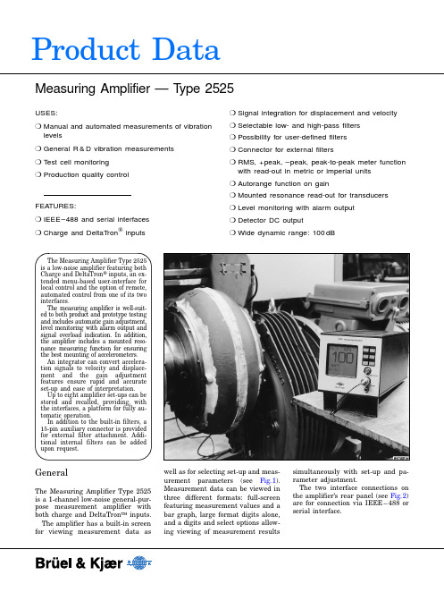
Product DataThe Measuring Amplifier Type 2525is a low-noise amplifier featuring both Charge and DeltaTron ® inputs, an ex-tended menu-based user-interface for local control and the option of remote,automated control from one of its two interfaces.The measuring amplifier is well-suit-ed to both product and prototype testing and includes automatic gain adjustment,level monitoring with alarm output and signal overload indication. In addition,the amplifier includes a mounted reso-nance measuring function for ensuring the best mounting of accelerometers.An integrator can convert accelera-tion signals to velocity and displace-ment and the gain adjustment features ensure rapid and accurate set-up and ease of interpretation.Up to eight amplifier set-ups can be stored and recalled, providing, with the interfaces, a platform for fully au-tomatic operation.In addition to the built-in filters, a 15-pin auxiliary connector is provided for external filter attachment. Addi-tional internal filters can be added upon request.Measuring Amplifier — Type 2525USES:r Manual and automated measurements of vibration levels r General R &D vibration measurements r T est cell monitoring r Production quality controlFEA TURES:r IEEE–488 and serial interfaces r Charge and DeltaT ron ® inputsr Signal integration for displacement and velocity r Selectable low- and high-pass filters r Possibility for user-defined filters r Connector for external filtersr RMS, +peak, –peak, peak-to-peak meter function with read-out in metric or imperial units r Autorange function on gainr Mounted resonance read-out for transducersr Level monitoring with alarm output r Detector DC outputr Wide dynamic range: 100dBGeneralThe Measuring Amplifier Type 2525is a 1-channel low-noise general-pur-pose measurement amplifier with both charge and DeltaTron ™ inputs.The amplifier has a built-in screen for viewing measurement data as well as for selecting set-up and meas-urement parameters (see Fig.1).Measurement data can be viewed in three different formats: full-screen featuring measurement values and a bar graph, large format digits alone,and a digits and select options allow-ing viewing of measurement resultssimultaneously with set-up and pa-rameter adjustment.The two interface connections on the amplifier’s rear panel (see Fig.2)are for connection via IEEE –488 or serial interface.Main FeaturesThe Measuring Amplifier Type 2525 includes a number of features which allow sophisticated and automatic measurement configuration as well as display set-up options which can be selected to best reflect the current application.Measurement Set-upThe measurement set-up consists of twelve menus which carry out (or lead to sub-menus which carry out) the following functions:r Measurement mode selection: ac-celeration, velocity displacement or forcer Transducer sensitivityr Input type: DeltaTron® or Charge (floating or grounded)r Input, output and fine gain select r Upper frequency limitr Lower frequency limitr Additional filter: internal or exter-nalr RMS averaging: exponential or lin-ear plus selectable averaging time r Peak hold timer Autorange (automatic gain adjust-ment)r Alarm On/Off, detector (RMS or peak), level, hold time and level exceed timer Detector DC outputDisplay Set-upMeasurement results can be dis-played in terms of RMS, positive or negative peak values, or peak-to-peak.Read-out value scales are selecta-ble as either absolute (with physical units shown) or dB. Bar graphs are shown with absolute values on a log-arithmic axis. Units can be specified as metric or imperial. Measurement values can be read-out in scientific notation (floating) or as fixed-point values (attenuator de-pendent).The Set-up Mode menu allows you to specify a full screen display which includes a bar graph of the current measurement as well as the instanta-neous measurement value, or the val-ues only. It is possible to make changes to the set-up while viewing their effect on the measurement values.General Set-up FeaturesIn addition to the measurement and display set-up features, a number of general options can be selected:r Select impulse frequency andread-out mounted resonance fre-quencyr Sine reference for sensitivity checkr Recall or store user-defined set-up,or recall factory set-upr Interface set-up: IEEE–488 ad-dress, serial baud rate, handshake,hardwired, modemr Back-lighting On/OffInterface ControlUnder the control of an external com-puting device via one of its two inter-faces, the amplifier’s extensivemeasurement and display featurescan be automated, allowing full inte-gration in a production line and au-tomated test environment.All features provided by the menusunder manual control (except thespecification of the interfaces them-selves) are also available via interface.In addition, interface control pro-vides some extra features with re-spect to resetting entire set-ups orindividual components, error hand-ling, and measurement and operationmonitoring and control.Fig.1 Measuring Amplifier Type 2525 front panel. The axes are not labelled as the displayis intended as a visual monitor onlyFig.2 Measuring Amplifier Type 2525 rear panel2Product and Prototype TestingAside from its sophisticated function-ality and possibilities for automated control, the Measuring Amplifier Type 2525 offers two main features which make it a must in the meas-urement chain of any automatedproduct test procedure:r Autorange (autogain)r Alarm monitoring functionThe autorange function makes set-ting up the amplifier easy in caseswhere you have little information re-garding the vibration levels themeasurement source can achieve.The alarm monitoring functionmakes it possible to select a monitor-ing level using RMS, positive or neg-ative peak values or peak-to-peak. Byspecifying a level exceed time, an ac-ceptable margin (e.g. noise margin)can be defined. The alarm hold timeensures that levels are held longenough to be discovered.CHARGE INPUT:Floating or grounded via TNC socket on front Max. Input 0 to 100kHz: 50nC peakMax. Common Mode Voltage on Floating Input: 5V peak at charge input level max. 10nC peak Common Mode Rejection Ratio (CMRR): With input gain +20 to +60dB:100Hz CMRR >60dB10kHz CMRR >45dBWith input gain –20 to +10dB:100Hz CMRR >50dB10kHz CMRR >40dBTotal Sensitivity:0.1pC to 10nC in steps of 10dB for 1V on AC output0.03pC to 10nC in steps of 0.01dB step for 1V on AC output, with reduced frequency rangeGain:Input Gain (before filtering and integration): Selectable from –20dB to +60dB in steps of 10dBVariable Gain (before filtering and integration): Selectable from 0dB to 11dB in steps of 0.01dB Output Gain (after filtering and integration): Selectable 0dB, 10dB and 20dBInherent Noise 2Hz to 22kHzSingle-ended: <5fC (<7fC @ 90% RH) Floating: <10fCon AC output, referred to input with maximum sensitivity, Lower Frequency Limit = 1Hz, and 1nF transducer capacitanceGain Accuracy (from input to AC output at 1kHz):Acceleration and force: Better than 2% Velocity: Better than 2.5%Displacement: Better than 3.0% @ 100Hz DeltaTron® INPUT:Via BNC socket on frontSensitivity:100µV to 10V in steps of 10dB for 1V on AC output30µV to 10V in steps of 0.01dB for 1V on AC output, with reduced frequency range Gain:Input Gain (before filtering and integration): Selectable from –20dB to +60dB in steps of 10dBVariable Gain (before filtering and integration): Selectable from 0dB to 11dB in steps of 0.01dBOutput Gain (after filtering and integration): Selectable 0dB, 10dB, 20dBGain Accuracy:Acceleration and force: Better than 2% Velocity: Better than 2.5%Displacement: Better than 3.0%Inherent Noise 2Hz to 22kHz:<20µV referred to input with maximum sensi-tivity and transducer output impedance <1kΩInput Impedance: >100kΩPower Supply for DeltaTron® Accelerometer: Constant Current: 4mA.Max Voltage on DeltaTron® input: 27V Out-of-range detection on DeltaTron® supply voltage (<3V or >21V)PREAMP OUTPUT:BNC socket on rearAcceleration signal after 1st order high-pass fil-ter, input gain and variable gain Max. Output: 5V peak (5mA peak)Output Impedance: 50ΩDC Offset: –50 <offset <+50mVAC OUTPUT:Via BNC socket on rearFully conditioned signalMax. Output: 5V peak (5mA peak)Output Impedance: 50ΩDC Offset: –10 <offset <+10mVFREQUENCY RANGE:Acceleration & Force:0.2Hz (better than –10% limit) to 100kHz (betterthan –20% limit)With variable gain selected: 0.2Hz to 40kHz(better than –10% limit)Velocity:1Hz to 10kHz (better than ±10% limits)Displacement:1Hz to 1kHz (better than ±10% limits)LOW–PASS FILTERS:2-pole Butterworth (maximally flat)Selectable –3dB limits of 1, 3, 10, 30kHz and OFFFilter Slope: 40dB/decadeAccuracy on –3dB Limit Freq.: ±5%, re 1kHzwithout filterHIGH-PASS FILTERS:3-pole Butterworth (maximally flat)Selectable –3dB limits of 0.1, 0.3, 1, 3, 10, 30Hzand OFFFilter Slope: 60dB/decadeAccuracy on –3dB Limit Freq.: ±10% (3, 10,30Hz), +10/−15% (0.1, 0.3, 1Hz), re 1kHz with-out filterADDITIONAL FILTERS:External filter connection via 15-pole D-sub-con-nector on rear.Optional custom internal filtering available on re-quest.External filter serially connected to standard fil-tersDISTORTION:<0.12% to 10kHz, <1% to 100kHzTEST OSCILLATOR:159.2Hz (=1000 rad/s), 100pC sinusoidal, ±1%SIGNAL RMS DECTECTOR:3 digits read out on LCDAccuracy for crest factor <3:Averaging Time:Exponential: 125ms, 1s, 10sLinear: 1s or 60s based on 125ms exp. val-uesSIGNAL PEAK DETECTOR:3 digits read out on LCD+Peak, –Peak:Settling time for a level shift from 0 to 3V onAC output:56µs (to –10% of value)72µs (to –5% of value)94µs (to –2% of value)Read-out (at AC output) value for a 3V peakof a period of one half sine with a (full period)frequency as listed:Max Peak Hold Time:0.5s to 60s in steps of 0.5s or infiniteMax peak reset functionDynamic range:+30mV to 3V on AC output (40dB)Peak-to-Peak:The numerical sum of +peak and –peak withextra hold time as described aboveOVERLOADS:Signal Overload:Peak overloading internal circuitsUpper 20dB:Indicates that at least one internal circuit is op-erating less than 20dB from overloadCM Overload:Common mode peak voltage >5V at floatingcharge inputDeltaTron® Overload:DeltaTron® supply voltage <3.0V or >21.0VGAIN AUTORANGE:None (manual gain setting)On output gain onlyOn input and output gainOVERLOAD RECOVERY TIME: <200µsTime for output to recover to within 250mV ofthe original value after termination of a half sinepulse of 50µs duration at the baseline. Pulseamplitude is 4 times the full scale input, peakACCELEROMETER MOUNTED RESONANCEMEASURING (EP patent 715.722, US patent5,753,793):Done via pulse method measuring. Excitingpulse ±15V, 3kHz to 60kHzCan be used with a number of Brüel&KjærCharge AccelerometersEXTERNAL FILTER:Connected between the internal filters and theoutput gainALARM FUNCTION:Level monitoring with alarm outputAlarm Output:In the 15-pole D-Sub socket on rear of amplifier Freq. RangeDynamic rangereferred to 1Von AC outputAccuracyreferredto input**1Hz to 10kHz+10dB to –30dB*±5%1Hz to 30kHz+10dB to –30dB*±10%1Hz to 100kHz+10dB to –20dB+10%–25%1Hz to 100kHz+10dB to –10dB+5%–20%For 60s linear averaging:*the dynamic range is +10 to −20dB**10% must be subtracted from the negativeaccuracy value (e.g. +5%, −15%, etc.)Sine FrequencyRead-out(% of FS peak value)1.0kHz–2%2.5kHz–8%5.0kHz–20%10.0kHz–40%Specifications 25253BP 1483–1499/06HEADQUARTERS: DK-2850Nærum·Denmark·Telephone:+4545800500·Fax:+4545801405·http://www.bk.dk·e-mail:**********Australia (02)9450-2066 · Austria 0043-1-8657400 · Brazil (011)5182-8166 · Canada (514)695-8225 · China (86)1068029906Czech Republic 02-67021100 · Finland (0)9-755 950 · France (01)69906900 · Germany 06103/908-5 6 · Hong Kong 25487486 · Hungary (1)2158305Ireland (01)4504922 · Italy (02)57604141 · Japan 03-3779-8671 · Republic of Korea (02)3473-0605 · Netherlands (0)30 6039994 · Norway 66771155Poland (22)8409392 · Portugal (1)4711453 · Singapore (65) 377-4512 · Slovak Republic 421754430701 · Spain (91)3681000 · Sweden (08)4498600 Switzerland 01/9436070 · Taiwan (02)7139303 · United Kingdom (0181)954-2366 · USA 180******** Local representatives and service organisations worldwideBrüel&Kjær reserves the right to change specifications and accessories without noticeOrdering InformationType 2525Measuring Amplifier Includes the following accessories:JP 0162:TNC to Microdot Adaptor AN 0010:Mains Cable VF 0032:T 630mA Fuse VF 0042:T 315mA Fuse LK 0014:Ferrite Cable Clamp VP 7758:Type 2525 Communication DemoProgramOptional AccessoriesAO 1382: 1.2m Microdot Accelerometer Cable, double screened for extra EMC protectionJP 1501:15-pole Sub-D Connector DH 0647:Housing for JP 1501JP 0145:BNC to Microdot Adaptor JP 0226:TNC to BNC AdaptorAO 0265:IEEE Interface Cables KK 0047:Frame for 19″ rackWH 3103:ISO 5349 Hand-arm filterWH 3267:900Hz to 1100Hz band pass filter WH 3112:A-weighting filterWH 3172:Whole body vibration z-filterRelay: SPDT, Max. 48V, 0.5A Alarm On/Off:Selectable via LCD and Interface bus Level:Selectable over the entire dynamic range. Mon-itoring will de-select while the autorange is changing gain (missing time periods after gain shifts)Level Exceed Time:Adjustable from 0 to 60s in steps of 1s Alarm Hold Time:Adjustable from 1 to 60s or infinite Alarm Reset Function Detector Type:Selectable RMS, +Peak, –Peak, Peak-to-Peak.Averaging/Hold time is transferred from detector set-up. Detectors are sampled at 125ms inter-vals (same interval as LCD meter digit updating)DETECTOR DC OUTPUT:In 15-pole D-Sub socket on rear V/unit: equal to V/unit for AC output Max Output: 3.5V (5mA peak)Output Impedance: 50ΩDC Offset: <±5mV Detector Type:Selectable RMS, +Peak, –Peak, Peak-to-Peak.Averaging/Hold time is transferred from detector set-upSampling Frequency:Output is updated at 125ms intervals (same in-terval as LCD meter digit updating). No curve fitting on outputIEEE –488 INTERFACE:The functions implemented conform to IEEE –488.1 and IEC 625–1 standards. Any function shown on display can be transmitted to and from the apparatus Functions Implemented:Source Handshake SH1Acceptor Handshake AH1Talker T6Listener L4Device Clear DC1Remote Local RL1SERIAL INTERFACE:Conforms to EIA/TIA–574 (“RS–232”)Baud Rate: 2400, 4800, 9600Parity: None Data Bits: 8Stop Bits: 1Handshake:X-On/X-Off, hardwired RTS/CTS, Modem DCDPower SupplyMains: 90V–127V or 200V–240V; 24VADimensions and WeightHeight : 132.5mm (5.22″)Width : 139.5mm (5.49″)Depth : 320mm (12.6″)Weight: 3.6kg (5.8lb.)Note: All values are typical unless measurement uncertainty or tolerance field is specified.Specifications 2525 (cont.)COMPLIANCE WITH STANDARDS:CE-mark indicates compliance with: EMC Directive and Low Voltage Directive.SafetyEN 61010–1 and IEC 1010–1: Safety requirements for electrical equipment for measurement, control and laboratory use.EMC EmissionEN 50081–1: Generic emission standard. Part 1: Residential, commercial and light industry.EN 50081–2: Generic emission standard. Part 2: Industrial environment.CISPR 22: Radio disturbance characteristics of information technology equipment. Class B Limits.FCC Rules, Part 15: Complies with the limits for a Class B digital device.EMC ImmunityEN 50082–1: Generic immunity standard. Part 1: Residential, commercial and light industry.EN 50082–2: Generic immunity standard. Part 2: Industrial environment. Note 1: The above is guaranteed using accessories listed in this Product Data sheet only.Note 2: See “EMC”TemperatureIEC 68–2–1 & IEC 68–2–2: Environmental Testing. Cold and Dry Heat.Operating Temperature: 5 to 40°C (41 to 104°F)Storage Temperature: –25 to +70°C (–13 to +158°F)Humidity IEC 68–2–3: Damp Heat: 90% RH (non-condensing at 40°C (104°F))MechanicalNon-operating:IEC 68–2–6: Vibration: 0.3mm, 20m/s 2, 10–500Hz IEC 68–2–27: Shock: 1000m/s 2IEC 68–2–29: Bump: 1000 bumps at 250m/s 2EnclosureIEC 529: Protection provided by enclosures: IP 20EMCSUSCEPTIBILITY TO DISTURBANCES SPECIFIED IN EN 50082–2:Measured using Accelerometer Cable AO 1382.Charge floating measurements according to User Manual with Ferrite Cable Clamp LK 0014mounted on accelerometer cable.At magnetic field 80A/m charge input noise can increase to 25fCRADIATED RF: (3 to 10V/m, 80% AM, 1kHz)CONDUCTED RF: (3 to 10V, 80% AM, 1kHz)1Measured with max. gain and 50Ω AC termination 2Measured with max. gain and 1nF terminationInput Radiated Conducted DeltaTron ®1<0.6mV<20µV Charge, single ended 2<0.3pC <0.02pC Charge, floating2<0.3pC<6pC。
12- 佳能iR 2525i 数码复印机佳能2525I A3 打印 复印 扫描一体机技术规范书

安徽省电力公司集中招标采购临泉供电公司佳能iR 2525i 数码复印机佳能2525I A3 打印复印扫描一体机技术规范书设计单位:临泉供电公司2011年3月单位:批准:审核:编制:2011年3月1日分标编号:货物需求一览表(买方填写)供货范围(卖方填写)1 总则产品总体要求:1、上述组件均为必配部件,供应商不得变更、调整、减少,应保证设备正常运行所应配置的相关辅件、组件。
2、必需符合中国CCC认证、能源之星认证、环保(绿色)认证要求,必需提供相关证明文件。
3、为保证供货渠道的合法性,需出具原厂商针对该项目的供货证明函原件和原厂针对本项目的专项授权函。
4、产品推荐:2、打印机需求基本参数复印/打印方式激光静电转印方式感光材料 OPC显影系统干式单组分显影定影系统按需定影内存标配 256MB(iR 2525)or512MB(iR 2520i/2525i/2530i/2535i/2545i)最大 512MB(iR 2525)预热时间主机电源打开时 30秒或更短睡眠模式恢复时 1秒最大原稿尺寸 A3首页输出时间 iR 2520i 6.4秒iR 2525i/2525/2530i 5.4秒iR 2535i/2545i 3.9秒灰度等级 256级分辨率扫描 600dpi×600dpi复印 1200dpi(等效)×600dpi打印真正1200dpi×1200dpi复印倍率固定倍率 25%,50%,61%,70%,81%,86%,115%,122%,141%,200%,400% 手动缩放 25%-400%(以1%为单位)连续输出速度 iR 2520i 20页/分钟(A4)iR 2525i/2525 25页/分钟(A4)iR 2530i 30页/分钟(A4)iR 2535i 35页/分钟(A4)iR 2545i 45页/分钟(A4)连续复印张数 999 张供纸量 iR 2520i/2525i/2525/2530i 标准 250张+550张(前置式纸盒)+100张(手送纸盘) 最大 250张+550张×3(前置式纸盒)+100张(手送纸盘)iR 2535i/2545i 标准 550张×2(前置式纸盒)+100张(手送纸盘)最大 550张×4(前置式纸盒)+100张(手送纸盘)纸张尺寸纸盒 A3-A5R、8K、16K和16KR手送纸盘 A3-A5R、8K、16K、16KR、非标准尺寸和信封纸张厚度纸盒 64-90g/m2手送纸盘 64-128g/m2出纸托盘容量 250张(A4)电源 iR 2520i/2525i/2525/2530i 220V AC_50Hz_3.3AiR 2535i/2545i 220V AC_50Hz_4.2A最大功耗 iR 2520i/2525i/2525/2530i 1.5kwiR 2535i/2545i 1.8kw主机尺寸 (宽×深×高) iR 2520i/2525i/2530i 565mm×693mm×896mm(安装有双面自动输稿器)iR 2525 565mm×680mm×806mm(安装有稿台盖板)iR 2535i/2545i 565mm×693mm×907mm(安装有双面自动输稿器)主机安装空间(宽×深) 1079mm×1441mm(不安装可选设备时)1367mm×1441mm(安装了可选的内置式装订器-B1时)重量 iR 2520i/2525i/2530i 约76.1kgiR 2525 约70.6kgiR 2535i/2545i 约78.4kg打印规格(标配)UFR II LT网络打印(标配)打印分辨率真正1200dpi×1200dpi打印语言 UFR II LT接口 100BASE-TX/10BASE-T、USB2.0高速网络协议 TCP/IP系统环境 Microsoft Windows?2000/XP/Vista/7,Server 2003/2008,Macintosh OS?(10.4或以上)PCL打印组件-AF1(选配)打印分辨率 1200dpi(等效)×600dpi打印语言 PCL5e, PCL6接口 100BASE-TX/10BASE-T、USB2.0高速网络协议 TCP/IP系统环境 Microsoft Windows?2000/XP/Vista/7,Server 2003/2008PS打印组件-AF1(选配)打印分辨率 1200dpi(等效)×600dpi打印语言 PS3仿真接口 100BASE-TX/10BASE-T、USB2.0高速网络协议 TCP/IP系统环境 Microsoft Windows?2000/XP/Vista/7,Server 2003/2008双面自动输稿器(仅限iR 2520i/2525i/2530i/2535i/2545i,iR 2525需选配)输稿速度 iR 2520i/2525i/2525/2530i 复印25页/分钟(A4,80g/m2)扫描25页/分钟(A4,80g/m2,黑白/彩色)iR 2535i/2545i 复印45页/分钟(A4,80g/m2)扫描30页/分钟(A4,80g/m2,黑白/彩色)原稿尺寸 A3-A5、8K、16K原稿厚度 iR 2520i/2525i/2525/2530i 50-105g/m2iR 2535i/2545i 52-128g/m2原稿托盘容量 iR 2520i/2525i/2525/2530i 50张(A4、80g/m2)iR 2535i/2545i 100张(A4、80g/m2)扫描规格扫描方式拉式标配推式 iR 2525选配色彩方式彩色/黑白扫描分辨率最大600dpi×600dpi(推式,黑白)生成格式 JPEG/TIFF/PDF/高压缩PDF(标配)/OCR PDF(需选配)传真规格(选配)Super G3传真卡-AG1适用线路公用电话线路1条线路调制解调速度 Super G3(最大33.6kbps)数据压缩方式 MH,MR,MMR,JBIG传输速度大约3秒/页 (33.6kbps)其它主要选购件内置式装订器-B1托盘数量 2个(主体本身标配一个,另外的附加内置装订托盘-B1需选配) 托盘容量标准托盘不分套、分套或分组模式 1000张或125mm(A4)装订模式 30套或125mm(A4)安装了附加托盘-B1 不分套、分套或分组模式 100张或12.5mm(A4)装订模式 15套或8.1mm(A4)最大装订张数 50张(A4,64-80g/m2)装订位置角落、两点内置式双路托盘-G1托盘数量 2个(包括一个主机托盘)托盘容量 100张(A4,80g/m2)双纸盒组件-AE1纸张容量 550张×2(80g/m2)纸张尺寸 A3-A5R、8K、16K纸张厚度 64-90g/m2耗材墨粉 NPG-50墨粉(印量约19,400页,用于iR 2535i/2545i)NPG-51墨粉(印量约14,600页,用于iR 2520i/2525i/2525/2530i)感光鼓 NPG-50/51感光鼓(印量约140,000页,用于iR 2535i/2545i) NPG-50/51感光鼓(印量约132,000页,用于iR 2520i/2525i/2525/2530i) 装订针-J1 角落装订、两点装订用针,5000支×3,用于内置式装订器-B1 佳能复印纸 A4 70g复印纸A3 70g复印纸A4 80g复印纸A3 80g复印纸2 测试和验收2.1 概述a 验收包括工厂验收和现场验收;b 投标方提供给招标方的所有设备必须在交货前通过工厂验收,并得到招标方的确认,若招标方未签署工厂验收报告,任何设备不能从投标方工厂发运;c 投标方应提供工厂验收和现场验收的测试程序的详细说明,测试项目和性能都应在详细说明中指出;d 招标方要求的一些特殊试验,只要合理都应进行;e 即使招标方在试验报告上签字,投标方仍应对设备固有缺陷和合同中的项目承担责任;f 测试和验收计划:投标方应提交有关工厂验收和现场验收的详细计划,包括系统性能和功能等的测试方法等,招标方有权修改测试和验收计划,在计划被招标方确认前,计划不应生效;g 测试设备:在工厂验收和现场验收中,投标方应提供验收过程中必需的设备,如检验设备、测量设备、记录设备等。
AS2525资料

Key Featuresq Line/speech handsfree circuit, LD/MF repertory dialler, and tone ringer on one 44 pin CMOS chip q Operating range from 15 to 100 mA line current (down to 5 mA with slightly reduced performance)q All significant parameters programmable with external EEPROM q Volume control of receiver signalq Handsfree function with enhanced voice switching q Low noise (max. -72 dBmp)q Unique EMC performanceq LD/MF switchable dialling with temporary MF mode q Repertory dialling with last number redial and memory dialling (8 x 2 direct and 10 indirect)q Call restriction with PIN codeq Serial interface for EEPROM and LCD driver q 2-tone/3-tone ringer with ring frequency detectionGeneral DescriptionThe AS2525 is a CMOS mixed-mode integrated circuit for use in feature phones, answering machines and fax machines. It contains an analogue line interface and speech circuit for a/b terminals,loudhearing, handsfree, enhanced LD/MF dialler, tone ringer with dc/dc converter and serial interface to EEPROM and LCD-driver (AS2591), all in a 44 pin package. The circuit is fully line powered.The AS2525 uses an external EEPROM for a 31 digit last number redial storage and memories for 26numbers each containing up to 21 digits/data.The device provides a volume control for the earpiece and the loudspeaker. The volume can be controlled by pressing the [V-]/[V+] keys.The versatility of the circuit is provided by programming all parameters through an external EEPROM. This allows easy adaptation to various PTT requirements worldwide.PackageAvailable in 44 pin TQFP.Austria Mikro Systeme International AGSingle-Chip Handsfree PhoneCMOS Integrated CircuitPin DescriptionPin #Symbol Type Description1CS2DO C hip S elect 2Chip select signal for external LCD driver circuit or 2 mA LEDIf signal is not activated, a pull down resistor ( 100 kΩ ) is inserted.2DPn DO D ial P ulse OutputDigital output which holds the line during off-hook operation or pulls low duringbreak periods of pulse dialling and flash.3HF DI H ands F ree Switch InputThis is an Schmitt-trigger input that is pulled high to enable handsfreeoperation.4HS DI H and S et Switch InputThis is an Schmitt-trigger input that is pulled high by the hook switch to enablehandset or headset operation.5FT1AI Analogue input pin for connecting a capacitor for offset cancellation.6FT2AI Analogue input pin for connecting a capacitor for offset cancellation.7M4AI M icrophone Input 4Differential input for the handsfree microphone (electret).8M2AI M icrophone Input 2Differential input for the handset microphone (electret).9M3AI M icrophone Input 3Differential input for the handsfree microphone (electret).10M1AI M icrophone Input 1Differential input for the handset microphone (electret).11STB AI S ide T one B alance InputAnalogue input for side tone cancellation network.12CS AO C urrent S hunt Control OutputN-channel open drain output to control the external high power shunt transistorfor synthesising ac- and dc-impedance, modulation of line voltage and shortingthe line during make periods of pulse dialling.Supply V oltage S ource S ource13VSSNegative Power Supply.14LI AI L ine I nputAnalogue input used for power extraction and line current sensing.15RI AI R eceive I nputAnalogue input for ac-separated receive signal.16SS AO S upply S ource Control OutputN-channel open drain output to control the external high power sourcetransistor for supplying (Vpp) the loudspeaker amplifier in off-hookloudspeaking/handsfree mode.17LS AI L ine Current S ense InputAnalogue input for sensing the line current.Pin #Symbol Type Description18CI AI C omplex I mpedance InputAnalogue input pin for the capacitor to program a complex impedance.19RECI AI REC eive I nputAnalogue input for the handsfree receive path. Should be connected to RO viaa coupling capacitor.20RECV AI REC eive V oice Switching InputAnalogue input for receive voice switching path.21RO AO R eceive O utput to H andsetOutput for driving a dynamic earpiece with an impedance from 150 Ω to 300 Ω. 22VDDSupply V oltage D rain D rainPositive Power Supply.23AGNDSupply A nalogue G rou ndSpecial ground for the internal amplifiers.24CBN AI Analogue input pin for connecting a capacitor for background noise monitoring. 25CM DO C onverter M ake OutputThis is an output for controlling the external switching converter. During ringingit converts the ring signal into a 4V supply voltage.26VPP Supply Loudspeaker Power SupplyHigh power supply for the output driver stage.27 28LO1LO2AO L oudspeaker O utputs1/2Output pins for a 32 Ω ( 25 to 50 Ω ) loudspeaker.29VSSASupply Power supply pin for LO1-LO2 output amplifier.30DM/HM DI D ial M ode/H eadset M ode Switch InputDigital input for choosing between LD and MF dialling or choosing handset andheadset mode. See “Table 3: Parameter settings” for further details. This pin isscanned after manual off-hook only.31FCI DI F requency C omperator I nputThis is a Schmitt-trigger input for ring frequency discrimination. Disabled duringoff-hook.32LED DO LED OutputDigital output for connecting 2 mA LED to indicate handsfree mode.33OSC O sc illator InputInput for ceramic resonator 3.58 MHz.34 35 36R1R2R3DI/O Keyboard R ows(see Figure 4: Keyboard Layout).37 38 39 40C1C2C3C4DI/O Keyboard C olumns(see Figure 4: Keyboard Layout).41CLK DO Cl oc kClock output for 3-wire bus.If signal is not activated, a pull down resistor (100 kΩ) is inserted.Pin #Symbol Type Description42DI DI D ata I nputData input of 3-wire bus.If signal is not activated, a pull down resistor (100 kΩ) is inserted.43DO DO D ata O utputData output of 3-wire bus.A 100 kΩ resistor connected from this pin to VSS enables key locking.If signal is not activated, a pull down resistor (100 kΩ) is inserted.44CS1DO C hip S elect 1Chip select signal for external EEPROM.If signal is not activated, a pull down resistor (100 kΩ) is inserted.DI:Digital Input AI:Analogue InputDO:Digital Output AO:Analogue OutputDI/O:Digital Input/Output AI/O:Analogue Input/outputPin ConfigurationKey Definitions and ProceduresTable 1: Key definitionsKey Condition Function Remark[0] - [9],[#], [∗]Off-hook Digits Function depending on mode[∗]LD mode Temporary MF select Providing mixed mode dialling (default LDselected)[PG]Speech mode Enter programme state To enter the programme stateProgramme mode Exit programme state To terminate/exit programme state [MT]Speech mode Enter mute state To enter mute stateMute state Exit mute state To terminate/exit mute stateProgramme mode Enter blank To enter blank digit during programming [R/P]Redial/Pause Allows re-signalling of the last dialled number andinsertion of pausesProgramme state Pause Each key pressure inserts a pause [FL]Flash function Invokes a timed loop break[V+]Speech mode Volume control To increase the receive gain[V-]Speech mode Volume control To increase or decrease the receive gain[MR]Memory redial key To access memory by key codes[M1] - [M8]Memory dial Access keys to memories 1 to 8 and 9 to 16 [SH]Second function (shift)To access second function of keysTable 2: DigitsDigit Key DTMF Mode(fLOW + fHIGH)Pulse Mode Programming Mode([PG] + Digit)Memory Location([MR] + Digit)[0]941 + 1336 Hz10 pulses Memory 17[1]697 + 1209 Hz 1 pulse To enter PIN protected programming Memory 18[2]697 + 1336 Hz 2 pulses Select flash duration Memory 19[3]697 + 1477 Hz 3 pulses Select dialling mode Memory 20[4]770 + 1209 Hz 4 pulses Select pause duration Memory 21[5]770 + 1336 Hz 5 pulses Key lock toggle Memory 22[6]770 + 1477 Hz 6 pulses Ringer volume Memory 23[7]852 + 1209 Hz7 pulses Ringer melody Memory 24[8]852 + 1336 Hz8 pulses LCD contrast Memory 25[9]852 + 1477 Hz9 pulses Ringer on/off Memory 26 [∗]941 + 1209 Hz Temporary MF select-[#]941 + 1477 Hz--Table 3: Parameter settings ParameterSymbol Procedure:[PG] + [0] + (Password) +Default OptionsInter-Digit Pause (LD)IDP [∗] + [1] + [HEX code]840 ms 1.72 ms … 7.03 sec. (see Table 4)MF Tone Duration TD [∗] + [2] + [HEX code]82 ms 1.72 ms … 7.03 sec. (see Table 4)MF Inter-Tone Pause ITP [∗] + [3] + [HEX code]82 ms 1.72 ms … 7.03 sec. (see Table 4)Flash 1 Duration FL1[∗] + [4] + [HEX code]101 ms 1.72 ms … 7.03 sec. (see Table 4)Flash 2 Duration FL2[∗] + [5] + [HEX code]285 ms 1.72 ms … 7.03 sec. (see Table 4)Pause 1 Duration P1[∗] + [6] + [HEX code] 1 second 1.72 ms … 7.03 sec. (see Table 4)Pause 2 Duration P2[∗] + [7] + [HEX code] 3 seconds 1.72 ms … 7.03 sec. (see Table 4)Pre-Digit Pause (LD)PDP [∗] + [8] + [HEX code]33 ms 1.72 ms … 7.03 sec. (see Table 4)Post Flash Pause PFP [∗] + [9] + [HEX code]274 ms 1.72 ms … 7.03 sec. (see Table 4)Tx Gain, Handset A TX-HS [0] + [1] + [HEX code]37 dB 30 to 45 dB (see Table 8)Rx Gain, Handset A RX-HS [0] + [2] + [HEX code] 1 dB -6 to 9 dB (see Table 12)Tx Gain, Handsfree A TX-HF [0] + [3] + [HEX code]46 dB 39 to 54 dB (see Table 10)Rx Gain, Loudspeaker A RX-HS [0] + [4] + [HEX code]29 dB 22 to 37 dB (see Table 14)Line LossCompensation LLC [0] + [5] +[0] = off [1] = range 1: I LINE = 20 - 50 mA [2] = range 2: I LINE = 45 - 75 mA DTMF Level (Low Group)V MF [0] + [6] + [HEX code]-6 dBm -18 to -6 dBm in 1 dB steps (see Table 24)Tx Gain, Headset A TX-HEAD [0] + [7] + [HEX code]37 dB 30 to 45 dB (see Table 20)Rx Gain, Headset A RX-HEAD [0] + [8] + [HEX code] 1 dB -6 to 9 dB (see Table 21)MF Comfort Tone, RO V MF-CT/RO [0] + [9] + [HEX code]-30 dBr -36 to -18 dBr in 6 dB steps (see Table 30)MF Comfort Tone,LO1/2V MF-CT/LO [0] + [0] + [HEX code]-9 dBr -15 to 3 dBr in 6 dB steps (see Table 30)Make/Break Ratio (LD)M/B [#] + [1] +[1] = 2 : 3[0] = 1 : 2Dial Rate (LD)DR [#] + [2] +[0] = 10 pps [1] = 20 pps DC Mask (LI Voltage)V LI[#] + [3] +[1] = 4.5 Volt [0] = 3.5 Volt Tx Soft Clip (Handset)[#] + [4] +[1] = on (2 V PEAK )[0] = off Rx Soft Clip (Handset)[#] + [5] +[1] = on (1 V PEAK )[0] = off Noise Monitoring (HF)[#] + [6] +[1] = on [0] = offLoudhearing Mode [#] + [7] +[1] = HF only [0] = LH and HF modes available Ringer Melody [#] + [8] +[1] = 3-Tone [0] = 2-Tone Key-in Tone (Beep)KT [#] + [9] +[1] = on [0] = offReset PIN Code [#] + [0] +[1] = 1111Selected by userParameter SymbolProcedure:[PG] + [0] + (Password) +Default Options Flash 1 During LD [#] + [∗] +[1] = on [0] = off Flash 2 During LD [#] + [#] +[0] = off [1] = on Extended LCD Symbols [9] + [1] +[0] = off [1] = on Tx Soft Clip,Handsfree [9] + [2] +[1] = on[0] = off Rx Soft Clip,Handsfree [9] + [3] +[1] = on [0] = offVoice Switching,Speed[9] + [4] +[1] = x 2[0] = x 1; [2] = x 4; [3] = x 8Handset/Headset Volume [9] + [5] +[1] = reset by on/off-hook[0] = setting is maintainedLCD Test[9] + [6]Turns on all segments, pressing any further key turns on all digits “1” and all symbols off.Temporary MF by ∗with tone[9] + [7] +[0] = off [1] = onKey Lock Function [9] + [8] +[1] =available [0] = not available Pin Select “DM/HM”DM/HM [9] + [9] +[1] = MF/LD [0] = Handset/Headset Ringer Off Function [9] + [0] +[1] =available[0] = not availableKey Test[9] + [∗] +Any key pressure turns the LED on Volume Control on Handset[9] + [#] +[1] = enabled[0] = disabledThe above parameters are programmable using a password (0123) through external EEPROM. All procedures must be terminated by pressing the [PG] key. Software for factory settings is available on request.The programming of timings is done by using a HEX data code as follows:Figure 5: Keys for HEX-code entry Data = 4096 - (f OSC /(512∗12) ∗ T(T = Time; f OSC = 3.58 MHz)Table 4: Timing selection by HEX codeParameter Default HEX Binary DataInter-digit pause 840 ms E171111 0001 0111Tone duration 82 ms FD01111 1101 0000Inter-tone pause82 ms FD01111 1101 0000Flash 1101 ms FC41111 1100 0100Flash 2285 ms F5A 1111 0101 1010Pause 1 1 sec DB91101 1011 1001Pause 2 3 sec 92C 1001 0010 1100Post-digit pause 33 ms FED 1111 1110 1101Post-flash pause274F601111 0110 0000Table 5: User programming with PIN code Function Symbol ProcedureOptionsCall Restriction 1CR1[PG] + [1] + (PIN) + [∗] + [1] +Key in two digits, use [MT] for blank Call Restriction 2CR2[PG] + [1] + (PIN) + [∗] + [2] +Key in two digits, use [MT] for blank Key Lock[PG] + [1] + (PIN) + [#] + [6] +[0] = unlocked and [1] = locked Clear All Memories [PG] + [1] + (PIN) + [#] + [7] +Press [1] to clear Reset To Factory Settings[PG] + [1] + (PIN) + [#] + [8] +Press [1] to resetChange PIN CodePIN [PG] + [1] + (PIN) + [0] +Key in new PIN + new PINPress [PG] to store setting and terminate procedureTable 6: Mode programming Function Symbol Procedure OptionsSelect Flash FL [PG] + [2] +[0] = Flash 1 and [1] = Flash 2Select Dialling Mode DM [PG] + [3] +[0] = LD (pulse)and [1] = MF (DTMF)Select Pause Time P[PG] + [4] +[0] = Pause 1 and [1] = Pause 2Easy Key Lock [PG] + [5] + [3] + [9]Toggles between locked and unlockedRinger Volume [PG] + [6] +[1] = -16 dB, [2] = -7 dB, and [3] = 0 dB (maximum)Ringer Melody [PG] + [7] +[0], [1], [2], [3], or [4]LCD Contrast V 33[PG] + [8] +[1], [2], or [3] (see also AS2591 data sheet)Bell On/Off[PG] + [9] +[0] = Off and [1] = OnPress [PG] to store setting and terminate procedureMemory AllocationThe EEPROM memory consists of three areas:Figure 6: Memory allocation for external EEPROMThe AS2525 is writing and reading to and from area B and C during normal operation and user-code programming.Area A is protected during normal operation and contains a back-up copy of the factory settings. This back-up copy can be loaded into area B by the user with the user-code programming procedure "reset to factory settings". The only way to change the factory settings in area A is by set-up programming using password. After changing area A by set-up programming, the AS2525 automatically performs a "reset to factory settings" to load this changes also into area B.Functional DescriptionDC ConditionsThe normal operating mode is from 15 mA to 100 mA. An operating mode with reduced performance is from 5 mA to 15 mA. In the line-hold range from 0 mA to 5 mA the device is in a power down mode.The dc characteristic is determined by the voltage at LI pin and a 30 Ω resistor between pin LI and LS. It can be calculated by the following equation:VLS = VLI+ ILINE∗ 30ΩVLIcan be programmed to be 3.5 V or 4.5 V.Table 7: DC mask selection[PG] + [0] + (Password) + [#] + [3] + (digit) + [PG] Digit DC Mask (dc voltage at pin LI)[0]Low dc mask, VLI= 3.5 Volt[1]High dc mask, VLI= 4.5 VoltFigure 7: DC characteristic with low dc mask2/4 Wire ConversionAS2525 has a built-in dual Wheatstone bridge with one common ground. This provides a maximum of independence of ac impedance and side-tone from each other. One can adapt side-tone without changing the ac impedance.AC ImpedanceThe ac impedance of AS2525 is set to 1000 Ω. A complex impedance can be adjusted by connecting an external capacitor to the CI pin. With an external resistor of approximately 1.5 kΩ connected to the LS pin, it can be programmed to 600 Ω.ZAC(syn) = 33∗ 30 ΩSide-ToneA good side-tone cancellation can be achieved byusing the following equation:ZBAL/ZLINE= 10This is assuming that the side-tone reference resistor,R2 (between LI and STB) is 300 Ω and R1 is 30 Ω.Figure 8: Side-tone balanceTransmit PathThe gain of the M1/M2 —> LS path is default set to37 dB. This gain can be changed from 30 dB to 45 dBin 1 dB steps by set-up programming.Table 8: Handset Tx gain setting[PG] + [0] + (Password) + [0] + [1] + (x) + [PG]Key(x)Tx Gain (dB)M1/2 to LSKey(x)Tx Gain (dB)M1/2 to LS[0]30[8]38[1]31[9]39[2)32[M1]40[3]33[M2]41[4]34[M3]42[5]35[M4]43[6]36[M5]44[7]37[M6]45The input is differential with an impedance of 10 kΩ.The soft clip circuit limits the output voltage swing atpin LS to 2 VPEAKwhen activated.Table 9: Handset Tx soft clipping selection[PG] + [0] + (Password) + [#] + [4] + (digit) + [PG]Digit Handset Tx Soft Clipping[0]Disabled[1]Enabled (2 VPEAK)There is optional LLC for this path.The gain of the M3/M4 —> LS path is default set to46 dB. This gain can be changed from 39 dB to 54 dBin 1 dB steps by set-up programming.Table 10: Handsfree Tx gain setting[PG] + [0] + (Password) + [0] + [3] + (x) + [PG]Key (x)Tx Gain (dB)M3/4 to LSKey(x)Tx Gain (dB)M3/4 to LS[0]39[8]47[1]40[9]48[2]41[M1]49[3]42[M2]50[4]43[M3]51[5]44[M4]52[6]45[M5]53[7]46[M6]54The input is differential with an impedance of 10 kΩ.The soft clip circuit limits the output voltage swing at pin LS to 2 VPEAKwhen activated.Table 11: Handsfree Tx soft clipping selection[PG] + [0] + (Password) + [9] + [2] + (digit) + [PG] Digit Handfree Tx Soft Clipping[0]Disabled[1]Enabled (2 VPEAK)There is no LLC option for this path.Receive PathThe gain of the LS —> RO receive path is default set to 1 dB. This gain can be changed from -6 dB to 9 dB in 1 dB steps by set-up programming.Table 12: Handset Rx gain setting[PG] + [0] + (Password) + [0] + [2] + (x) + [PG]Key (x)Rx Gain (dB)LS to ROKey(x)Rx Gain (dB)LS to RO[0]-6[8]2[1]-5[9]3[2]-4[M1]4[3]-3[M2]5[4]-2[M3]6[5]-1[M4]7[6]0[M5]8[7]1[M6]9The user can also change the gain within this range in 4 dB steps via the [V+]/[V-] keys. The receive default gain in handset and headset mode must lie between position 5 and 9 for correct operation of the volume control. The receive input is the differential signal of RI and STB. The soft clip circuit limits the output voltage at RO to 1 VPEAK. It prevents harsh distortion and acoustic shock.Table 13: Handset Rx soft clipping selection[PG] + [0] + (Password) + [#] + [5] + (digit) + [PG] Digit Handset Rx Soft Clipping (Earpiece)[0]Disabled[1]EnabledThere is LLC option for this path.The gain of the LS —> LO1/LO2 receive path is set to 29 dB.This gain can be changed by set-up programming from 22 dB to -37 dB in 1 dB steps.Table 14: Loudspeaker gain setting[PG] + [0] + (Password) + [0] + [4] + (x) + [PG] Key(x)Rx Gain (dB)LS to LO1/2Key(x)Rx Gain (dB)LS to LO1/2[0]22[8]30[1]23[9]31[2]24[M1]32[3]25[M2]33[4]26[M3]34[5]27[M4]35[6]28[M5]36[7]29[M6]37The user can also change the gain using the [V+]/[V-] keys (see section "Handsfree"). The volume range is 15 dB (-7/+8 dB).The receive input is the differential signal of RI and STB. The soft clip circuit limits the output voltage swing at LO1/LO2 to 1 VPEAK.Table 15: Loudspeaker soft clipping selection[PG] + [0] + (Password) + [9] + [3] + (digit) + [PG] Digit Handfree Rx Soft Clipping (Loudspeaker)[0]Disabled[1]EnabledThere is optional LLC for this path.Line Loss Compensation (LLC)The line loss compensation is set-up programmable and effects only the handset mode.Table 16: Line loss compensation selection[PG] + [0] + (Password) + [0] + [5] + (digit) + [PG]Digit LLC Range[0]No LLC (gain independent of line current)[1]-1 dB/5 mA from 20 to 50 mA [2]-1 dB/5 mA from 45 to 75 mAWhen it is activated, the transmit and receive gains for both channels are decreased by 6 dB at line currents from 20 mA to 50 mA or from 45 mA to 75 mA depending on selected range.HandsfreeThe handsfree function allows voice communication without using the handset (full 2-way speaker phone).Two voice controlled attenuators prevent acoustic coupling between the loudspeaker and the handsfree microphone.The voice switching circuit has three states, namely idle, transmit or receive. In receive mode the attenuation of the receive path and the transmit path can be controlled by the volume keys between 0 dB and -15 dB. The following table (Table 18: Handsfreeattenuation scheme) shows how voice switching is controlled.Figure 9: Handsfree voice switchingA background monitoring circuit is incorporated. This circuit can be enabled/disabled as required.Table 17: Background noise monitoring selection [PG] + [0] + (Password) + [#] + [6] + (digit) + [PG]Digit Background Noise Monitoring [0]Disabled [1]EnabledFigure 10: Signal path of handsfree circuitTable 18: Handsfree attenuation schemeSpeechMode RX-gain TX-gain RemarkRX > TX_attenXReceive0 dB to -20 dB-50 dB to -30 dBadjustable with [V+]/[V-] keys in 8stepsTX_atten > RX No Idle -25 dB -25 dBmiddle positionTX_atten > RX Yes Transmit -50 dB 0 dB independent of [V+]/[V-] keysFigure 11: Gain transition of voice switchingLoudhearingA loudhearing mode can be enabled/disabled through the set-up programming.Table 19: Loudhearing mode selection[PG] + [0] + (Password) + [#] + [7] + (digit) + [PG]Digit Loudhearing[0]Enabled (LH + HF provided)[1]Disabled (only HF is provided)Headset modeHead set mode is selected by connecting pin "HEAD"to V DD and enabling the head function by service code programming (see also Table 3: Parameter settings).Table 20: Headset Tx gain setting[PG] + [0] + (Password) + [0] + [7] + (x) + [PG]Key (x)Tx Gain (dB)M1/2 to LSKey (x)Tx Gain (dB)M1/2 to LS[0]30[8]38[1]31[9]39[2]32[M1]40[3]33[M2]41[4]34[M3]42[5]35[M4]43[6]36[M5]44[7]37[M6]45Table 21: Headset Rx gain setting[PG] + [0] + (Password) + [0] + [8] + (x) + [PG]Key (x)Rx Gain (dB)LS to ROKey(x)Rx Gain (dB)LS to RO[0]-6[8]2[1]-5[9]3[2]-4[M1]4[3]-3[M2]5[4]-2[M3]6[5]-1[M4]7[6]0[M5]8[7]1[M6]9If this mode is entered both hook inputs HS and HF act as electronic off-hook for handset operation. The gain in transmit and receive can be programmed by service code programming. The pin "HEAD" is only scanned once after off-hook and any change on this pin during one session will be ignored.Ring Frequency DetectionThe ring frequency detector assures that only signals with a frequency between 13 Hz and 70 Hz are regarded as valid ring signals.When a valid ring signal is present for 100 ms continuously, the melody generator is activated and remains active as long as the ring signal is present. Once the melody generator has been started, the ring signal is continuously monitored and the melody generator is instantly turned on or off according to the momentary presence of a valid or invalid ring signal respectively (until next POR or off-hook).DC/DC converterWhen a valid ring signal is detected, the dc/dc converter is started.Dialling and Control FunctionsValid KeysThe key scanning is enabled in off-hook mode with V DD above V REF . A valid key is detected from the keyboard by connecting the appropriate row to the column (R ON < 1 k Ω). This can be done using an n x m keyboard matrix with single contacts. Three diodes and a resistor are used to extend the number of rows (see Figure 4: Keyboard Layout).PIN CodeA PIN code is available for protection various user settings. The default PIN code is set to 1111 and can be change as follows:1. Press [PG] to enter programme mode2. Press [1] + (PIN) + [0]3. Key in new PIN code (valid digits: 0 - 9, #)4. Key in new PIN code again5. Press [PG] (= store and exit) or go on-hook to abortIt is also possible to reset the PIN code through set-up programming:1. Press [PG] to enter programme mode2. Press [0) + (Password) + [#] + [0]3. Press [1] to reset4. Press [PG] (= store and exit) or go on-hook to abortCall RestrictionA call restriction function is accommodated. This function can be activated using the PIN code.Storing digits for call restriction:1. Press [PG] to enter programme mode2. Press [1] + (PIN) + [∗]3. Press [1] for first call restriction and [2]for second call restriction4. Key in digits for call restriction (2 digits,[MT] for blank)5. Press [PG] (= store and exit) or go on-hook to abort.Key LockA key lock function is provided to allow the user to protect the telephone from any mis-use. When this function is available through the set-up programming,it is possible to enable/disable the key lock using the user PIN code.Enabling/disabling key lock:1. Press [PG] to enter programme mode2. Press [1] +(PIN) + [#] + [6]3. Press [1] for enable or [0] for disable4. Press [PG] (= store and exit) or go on-hook to abortAlso an easy key lock function is provided. This function can be activated/disactivated when the key lock function is available through set-up programming and the previous mentioned key lock through PIN code is disabled.Clear Memory ProcedureIt is possible to clear all stored numbers by using the PIN code as follows:1. Press [PG] to enter programme mode2. Press [1) + (PIN) + [#] + [7]3. Press [1] for clear4. Press [PG] (= store and exit) or go on-hook to abortReset to Factory SettingsIt is possible to reset all settings to the default factory settings with following procedure:1. Press [PG] to enter programme mode2. Press [1] + (PIN) + [#] + [8]3. Press [1] for reset4. Press [PG] (= store and exit) or go on-hook to abortDial Mode SelectionThe default signalling mode (LD or MF) is selectable through following procedure:1. Press [PG] to enter programme mode2. Press [3] to enter dial select mode3. Press [0] for LD and [1] for MF4. Press [PG] (= store and exit) or go on-hook to abortWhen default LD mode is selected, a temporary change to MF can be invoked by pressing the [∗] key. Temporary MF select with tone on first key pressure can be selected as option (see also Table 3: Parameter settings). The circuit will revert to LD by pressing the [FL] key or by next on-hook.Re-Dialling (Last Number Redial)Re-dialling is a facility that allows re-signalling of the last dialled number without keying in all the digits again. Numbers dialled out from any memory will also be stored in the LNR memory. The re-dialling works in following manner:• Any digit (including Flash, Pause, and MF select) being dialled is storable in the LNR memory up toa total of 31 digits.• If more than 31 digits are entered, re-dialling will be inhibited.• Pressing the [R/P] key as first entry after off-hook (LNR cursor at first digit) will invoke dialling the content of the LNR memory.• If the [R/P] key is pressed after entering one or more digits, the key will function as a pause key and each pressure will insert a pause.Pauses can also be inserted by pressing the [R/P] key in programme mode.Flash FunctionA flash, [FL] key, activation will invoke a timed loop break. The flash duration can be programmed through set-up (see Figure 5: Keys for HEX-code entry and Table 4: Timing selection by HEX code):Table 22: Flash duration setting[PG] + [0] + (Password) + [∗] + (digit) + (HEX) + [PG] Digit Timing Flash Duration[4]HEX code Flash 1[5]HEX code Flash 2One of two pre-programmed can be selected as follows:1. Press [PG] to enter programme mode2. Press [2] to enter flash select mode3. Press [0] for duration 1 and [1] forduration 24. Press [PG] (= store and exit) or go on-hook to abortA flash entered will be stored in the LNR memory together with entered digits. After a recall a 270 ms pause will automatically be executed.PausesPauses can be inserted if the [R/P] key is pressed after entering one or more digits. Also during programming, pauses can be inserted by pressing the [R/P] key. Default pause duration is 1 second (P1) and an alternative pause of 3 second (P2) can be selected. These pauses can be changed through the set-up programming (see Table 3: Parameter settings)Memory KeysThe keys [M1] to [M8]are direct memory access keys, [SH] key is used to access second level of direct memories, and the [MR) key is used for key-code dialling. Up to 26 numbers can be stored in the on-chip RAM. Each number can contain up to 21 digits (including pauses).During programming multiple pauses can be inserted by pressing the [RD] key.Example (45678P123 is stored in M1, where P is a pause and 123 the extension number):1. Off-hook, wait for dial tone2. Press [M1]• 45678 is dialled out• Dialling halts (pauses)• Dialling is resumed, 123 is dialled out.。
- 1、下载文档前请自行甄别文档内容的完整性,平台不提供额外的编辑、内容补充、找答案等附加服务。
- 2、"仅部分预览"的文档,不可在线预览部分如存在完整性等问题,可反馈申请退款(可完整预览的文档不适用该条件!)。
- 3、如文档侵犯您的权益,请联系客服反馈,我们会尽快为您处理(人工客服工作时间:9:00-18:30)。
Document Number: 34177
For technical questions, contact: magnetics@
IHLP-2525EZ-01
Vishay Dale
Low Profile, High Current Inductor
FEATURES
•Shielded construction
•Frequency range below 1 MHz •Lowest DCR/µH, in this package size
•
•Handles high transient current spikes without hard saturation
•Ultra low buzz noise, due to composite construction
•100 % lead (Pb)-free and RoHS compliant
APPLICATIONS
•Notebook/Desktop/Server applications •High current POL converters
•Low profile, high current power supplies •Battery powered devices
•DC/DC converters in distributed power systems
•DC/DC converter for Field Programmable Gate Array (FPGA)
Manufactured under one or more of the following:
US Patents; 6,198,375/6,204,744/6,449,829/6,460,244. Several foreign patents, and other patents pending.
NOTES:
1. All test data is referenced to 25 °C ambient.
2. Operating Temperature Range - 55 °C to + 125 °C
3. DC current (A) that will cause an approximate ΔT of 40 °C.
4. DC current (A) that will cause Lo to drop approximately 20 %
5. The part temperature (ambient + temp rise) should not exceed 125 °C under worst case operating conditions. Circuit design, component placement, PWB trace size and thickness, airflow and other cooling provisions all affect the part temperature. Part temperature should be verified in the end application.
STANDARD ELECTRICAL SPECIFICATIONS
Lo
INDUCTANCE µH ± 20 % at 100 kHz 0.25 V , 0 A DCR m Ω TYPICAL 25 °C
DCR
m Ω
MAX 25 °C HEAT
RATING CURRENT DC AMPS 3 TYPICAL SATURATION CURRENT DC AMPS 4TYPICAL
0.56 3.4 3.620120.68 4.2 4.51811.50.82 4.6 4.916.5131.0 5.6 6.513151.58.69.012122.213.013.610103.319.920.9884.728.930.3 6.575.632.734.4676.842.544.6 5.5 5.58.2
43.5
45.6
5.5
5.5
10.067.971.3 4.5 4.5
For technical questions, contact: magnetics@
Document Number: 34177
IHLP-2525EZ-01
Vishay Dale
Low Profile, High Current Inductor
IHLP-2525EZ-01
Low Profile, High Current Inductor
Vishay Dale
Document Number: 34177For technical questions, contact: magnetics@
Disclaimer Legal Disclaimer Notice
Vishay
All product specifications and data are subject to change without notice.
Vishay Intertechnology, Inc., its affiliates, agents, and employees, and all persons acting on its or their behalf (collectively, “Vishay”), disclaim any and all liability for any errors, inaccuracies or incompleteness contained herein or in any other disclosure relating to any product.
Vishay disclaims any and all liability arising out of the use or application of any product described herein or of any information provided herein to the maximum extent permitted by law. The product specifications do not expand or otherwise modify Vishay’s terms and conditions of purchase, including but not limited to the warranty expressed therein, which apply to these products.
No license, express or implied, by estoppel or otherwise, to any intellectual property rights is granted by this document or by any conduct of Vishay.
The products shown herein are not designed for use in medical, life-saving, or life-sustaining applications unless otherwise expressly indicated. Customers using or selling Vishay products not expressly indicated for use in such applications do so entirely at their own risk and agree to fully indemnify Vishay for any damages arising or resulting from such use or sale. Please contact authorized Vishay personnel to obtain written terms and conditions regarding products designed for such applications.
Product names and markings noted herein may be trademarks of their respective owners.
元器件交易网。