MAX6392KA26中文资料
MAX9632-MAX9633低噪音
MAX9632/MAX9633 低噪音
Maxim 的新轨至轨运算放大器提供高电压性能在低频率,精确的规格,高收益,能够在工业应用精密的信号调理。
位于美国加州Sunnyvale,2010 年11 月9 日,MAXIM 集成产品公司(NASDAQ:MXIM)推出MAX9632/MAX9633 的36V,低噪音,低失真精密运算放大器。
在Maxim 的高电压,精密运算放大器新系列的第一个器件,MAX9632/MAX9633 的设计采用了一个专有的高速互补BiCMOS 工艺
(CB5HV)。
这个高电压模拟工艺优化交流优秀的动态性能,超低噪声,工作电压范围宽,低漂移信号调理。
MAX9632/MAX9633 目标的工业数据采集系统的精度要求在低频信号调理。
在MAX9632 是单运放具有超低输入电压噪声密度0.94nV /,低偏移的125μV(最大值),和偏移量温度系数的0.5μV/° C(最大)。
在MAX9633 是一款双用的3nV 输入电压噪声密度运算放大器/,对200μ偏移(最大)一,和偏移量温度系数的0.9μV/° C(最大)。
这两款器件提供高规格的信号保真度和总谐波失真调节优于-一三六分贝,能够在专业音响设备和高端测试和仪器仪表应用。
增益带宽积(GBWP)是典型的MAX9632 和MAX9633 27MHz 时为55MHz 的。
这可用带宽,慷慨的4.5V 至36V 工作电压范围,典型的三点九毫安(MAX9632)电流消耗相结合,。
2SA966资料

TOSHIBA Transistor Silicon PNP Epitaxial Type (PCT Process)2SA966Audio Power Amplifier Applications• Complementary to 2SC2236 and 3-W output applications.Absolute Maximum Ratings (Ta = 25°C)Characteristics Symbol Rating UnitCollector-base voltage V CBO −30 V Collector-emitter voltage V CEO −30 V Emitter-base voltage V EBO −5 V Collector current I C−1.5 AEmitter currentI E 1.5 A Collector power dissipation P C 900 mW Junction temperature T j 150 °C Storage temperature rangeT stg−55 to 150°CNote: Using continuously under heavy loads (e.g. the application of high temperature/current/voltage and the significant change in temperature, etc.) may cause this product to decrease in thereliability significantly even if the operating conditions (i.e. operating temperature/current/voltage, etc.) are within the absolute maximum ratings.Please design the appropriate reliability upon reviewing the Toshiba Semiconductor Reliability Handbook (“HandlingPrecautions”/Derating Concept and Methods) and individual reliability data (i.e. reliability test report and estimated failure rate, etc).Unit: mmJEDEC TO-92MOD JEITA ―TOSHIBA 2-5J1A Weight: 0.36 g (typ.)Electrical Characteristics (Ta = 25°C)Characteristics Symbol TestCondition MinTyp.Max UnitCollector cut-off current I CBO V CB = −30 V, I E = 0 ――−100nAEmitter cut-off current I EBO V EB = −5 V, I C = 0 ――−100nA Collector-emitter breakdown voltage V (BR) CEO I C = −10 mA, I B = 0 −30 ―― V Emitter-base breakdown voltage V (BR) EBO I E = −1 mA, I C = 0 −5 ―― VDC current gain h FE(Note)V CE = −2 V, I C = −500 mA 100 ― 320Collector-emitter saturation voltage V CE (sat)I C = −1.5 A, I B = −0.03 A ――−2.0V Base-emitter voltage V BE V CE = −2 V, I C = −500 mA ――−1.0V Transition frequency f T V CE = −2 V, I C = −500 mA ― 120 ― MHz Collector output capacitance C ob V CB = −10 V, I E = 0, f = 1 MHz ― 40 ― pF Note: h FE classification O: 100 to 200, Y: 160 to 320Markinglead (Pb)-free package orlead (Pb)-free finish.indicatorCollector current I C (mA)h FE – ICD C c u r re n t g a i n h F ECollector current I C (mA)V CE (sat) – I CC o l l e c t o r -e m i t t e r s a t u r a t i on v o l t a g eV C E (s a t ) (V )Base-emitter voltage V BE (V)I C – V BEC oll e c t o rc u r r e n t I C (m A )Ambient temperature Ta (°C)P C – TaC o l l e c t o r p owe r d i s s ip a t io n P C (W )Collector-emitter voltage V CE (V)Safe Operating AreaC o l l e c t o r c u r r e n t I C (A )1.00 0 20 40 60 80 100 120 140 160 1800.20.40.60.8−−−−−−−−−−−−−−−−−−Collector-emitter voltage V CE (V)I C – V CEC o l l e c t o r c u r r e n t I C (m A )−−−−−−−−−−−−−−−−−RESTRICTIONS ON PRODUCT USE20070701-EN •The information contained herein is subject to change without notice.•TOSHIBA is continually working to improve the quality and reliability of its products. Nevertheless, semiconductor devices in general can malfunction or fail due to their inherent electrical sensitivity and vulnerability to physical stress. It is the responsibility of the buyer, when utilizing TOSHIBA products, to comply with the standards of safety in making a safe design for the entire system, and to avoid situations in which a malfunction or failure of such TOSHIBA products could cause loss of human life, bodily injury or damage to property.In developing your designs, please ensure that TOSHIBA products are used within specified operating ranges as set forth in the most recent TOSHIBA products specifications. Also, please keep in mind the precautions and conditions set forth in the “Handling Guide for Semiconductor Devices,” or “TOSHIBA Semiconductor Reliability Handbook” etc.• The TOSHIBA products listed in this document are intended for usage in general electronics applications (computer, personal equipment, office equipment, measuring equipment, industrial robotics, domestic appliances, etc.).These TOSHIBA products are neither intended nor warranted for usage in equipment that requires extraordinarily high quality and/or reliability or a malfunction or failure of which may cause loss of human life or bodily injury (“Unintended Usage”). Unintended Usage include atomic energy control instruments, airplane or spaceship instruments, transportation instruments, traffic signal instruments, combustion control instruments, medical instruments, all types of safety devices, etc.. Unintended Usage of TOSHIBA products listed in his document shall be made at the customer’s own risk.•The products described in this document shall not be used or embedded to any downstream products of which manufacture, use and/or sale are prohibited under any applicable laws and regulations.• The information contained herein is presented only as a guide for the applications of our products. No responsibility is assumed by TOSHIBA for any infringements of patents or other rights of the third parties which may result from its use. No license is granted by implication or otherwise under any patents or other rights of TOSHIBA or the third parties.• Please contact your sales representative for product-by-product details in this document regarding RoHS compatibility. Please use these products in this document in compliance with all applicable laws and regulations that regulate the inclusion or use of controlled substances. Toshiba assumes no liability for damage or losses occurring as a result of noncompliance with applicable laws and regulations.。
5.2.1 国外品牌手机话机锁解锁指令及方法速查[共5页]
![5.2.1 国外品牌手机话机锁解锁指令及方法速查[共5页]](https://img.taocdn.com/s3/m/75ef786e1a37f111f0855b5f.png)
第5章手机解锁指令及方法速查131续表品牌型号其他解密功能及方法康佳C928、C936……需要使用解锁软件才能解开话机锁。
另外,C958、C968、A06、A98、D108、R608、R718、KC66、KC88、KC627、KC826等型号手机的解锁方法也相同K5238 输入指令“*5238*00#”可解个人信息密码琐3288 输入解锁指令“*6608866#”可解个人信息密码锁5238 输入解锁指令“*5238*00#”可解个人信息密码锁科健3000 输入指令“*#9918*106*1647#”或“*#9918*106*6538#”即可解决不能使用充值卡充值的问题美辰系列型号可使用串号解锁法,打开串号解锁软件,输入手机串号(格式是“******—**—******—*”,其中横杠是空格),输入正确后按“回车”键即可计算出锁机码,即界面第4行的后8位数,然后开机输入“#9917*”+8位解锁码+“#”即可恢复出厂设置并解锁首信C5066、C5068、C5288……输入指令“*#9922#”(无卡),可看settsing(设置)输入指令“*#9999#”可使手机复位,输入指令“*#06#”可查看串号另外,C6268、C6568等型号手机的指令也相同厦华2000 长按“C”键可以消除屏幕右下角的笑脸5.2 国外品牌手机解锁指令5.2.1 国外品牌手机话机锁解锁指令及方法速查品牌型号话机锁解锁指令及方法阿尔卡特BE4、BE5输入指令“83227423”即可解开话机锁另外,OT301、302、303等型号手机的解锁指令和方法也相同HD1、HE1输入指令“25228352”即可解开话机锁,输入指令“###847#”也可解锁。
另外,OT500、700等型号手机的解锁指令和方法也相同OT501 输入指令“###847#”即可解开话机锁,另外,OT511等型号手机的解锁指令和方法也相同OT735 输入指令“83227423”即可解开话机锁,另外,535等型号手机的解锁指令和方法也相同爱立信T36、T28 输入指令“*#0000#”即可将爱立信老型号手机的菜单恢复到英语菜单,同时解开话机锁388、398 在手机显示“phone locked”或“话机已锁”时,只要输入指令“0000”,即可解开话机锁飞利浦系列型号在待机状态下,输入指令“*#7489*#”,即可显示和更改手机密码并解锁另外,DIGA、GENIE系列手机的解锁指令和方法也相同FIZZ 输入指令“*#1234*#”可以查看密码并解开话机锁S568 输入指令“*01763*737381#”即可解开话机锁168C 输入指令“*#2254*#”即可解开话机锁630 输入指令“#20021208”按“发射”键即可解开话机锁828 输入指令“*#7489*#”即可通过显示和更改手机密码进行解锁泛泰PG8000 输入指令“*01763*737381#”即可解开话机锁7870 不装卡输入指令“*4955#”后,手机进入工程模式,选择消除所有密码,即可解开CPU锁好彩K896输入指令“*2580*#”(第一个“*”要按两次,否则按不出来),进入手机测试模式,选择恢复出厂设置,即可解开话机锁338输入指令“**2580*#”进入手机工程模式,选择第6项码片复位,即可解开话机锁(同时会清除手机中的电话号码,最好用试机卡)韩国蓝星 V268……插卡开机后输入指令“0124”即可解开话机锁另外,V268+等型号手机的解锁指令和方法也相同LG GSM全系列不插卡开机输入指令“2945#*#”,选第6项Factory Reset(恢复出厂值),即可解开话机锁,这个方法还可以解决一些手机的开机定屏问题(通常出现在不插卡正常,插卡定屏的那些型号上)ALL……输入指令“2945#*#”即可解开话机锁另外,LG 2G等型号手机的解锁指令和方法也相同。
莫卡(Moxa)产品说明书
Copyright © 2017 Moxa Inc. Released on December 28, 2017About MoxaMoxa is a leading manufacturer of industrial networking, computing, and automationsolutions. With over 25 years of industry experience, Moxa has connected more than 30 million devices worldwide and has a distribution and service network that reachescustomers in more than 70 countries. Moxa delivers lasting business value by empowering industry with reliable networks and sincere service for automation systems. Information about Moxa’s solutions is available at . You may also contact Moxa by email at *************. How to Contact Moxa Tel: +886-2-8919-1230 How to Use the TIA Portal to Set a Siemens PLC and the MGate 5111Moxa Technical Support Team****************Contents1 Application Description ...................................................................2 2 System Topology .............................................................................3 3Required Equipment and Components (4)A. TIA Portal .................................................................................................... 4B. Modbus Slave .............................................................................................. 4C.MGate 5111 Firmware (4)D. MGate 5111’s GSD File (4)4MGate 5111 Setting (5)A. Protocol Conversion ...................................................................................... 5B. Configure Modbus Commands ........................................................................ 5C.Configure PROFIBUS Module (7)D. I/O Data Mapping (8)5 Siemens PLC Setting ....................................................................... 9 6Communication Test (21)A. Status Monitoring ........................................................................................21 B. Fault Protection . (27)1Application DescriptionThe TIA Portal is Siemens’s new software platform to configure and programS7-300/400/1200/1500 PLCs. This technical note demonstrates how to configure theSiemens S7-300 to connect with the MGate 5111 in TIA Portal V14.The MGate 5111 supports a variety of maintenance functions, such as Protocol Diagnostics, Traffic Monitoring, Status Monitoring, and Fault Protection. The Status Monitoringfunction notifies a PLC/DCS/SCADA system when a Modbus device gets disconnected or does not respond. If a command has run successfully, the status bit’s value will be 1. If a command has failed, the status bit’s value will be 0. In this case, the master device will be aware of the failure status of the slave device. When a PROFIBUS cable gets disconnected, the Fault Protection function executes actions on end devices identified by a pre-defined value set by the user.This technical note demonstrates how PROFIBUS Master (Siemens PLC) get these Modbus command statuses by receiving Input Status module values, as well as how the FaultProtection function works. We also demonstrate how Protocol Diagnostics and TrafficMonitoring make troubleshooting easy.2System TopologyThis technical note demonstrates how to exchange data between a PROFIBUS master and six Modbus TCP slaves. The Modbus TCP slave IDs 1-3 use Modbus Read command and show the Status Monitoring function. The Modbus TCP slave IDs 4-6 use Modbus Write command and show the Fault Protection function.We use the Siemens S7-300 as the PROFIBUS Master to connect the MGate 5111’s PROFIBUS port. On a PC, we run a Modbus Slave tool to simulate Modbus TCP slaves that the MGate 5111 will connect to the PC’s TCP 502 to poll slaves.3Required Equipment and ComponentsA.TIA PortalAs a registered Siemens’s customer you can download the trial software for TIA PortalV14 and test it for 21 days.Version: V14Download Website:https:///cs/document/109740158/simatic-step-7-(tia-portal)-v14-trial-download?dti=0&lc=en-WWB.Modbus SlaveModbus Slave is a popular Modbus slave simulator to test and debug your modbusdevices. Supports Modbus RTU/ASCII and Modbus TCP/IP.Version: V6+Download Website:/download.htmlC.MGate 5111 FirmwareVersion: V.1.0Download Website: D.MGate 5111’s GSD FileThe GSD (General Station Description) file is an electronic device datasheet or device database file that identifies the PROFIBUS IO device. This file can be installed into a PROFIBUSEngineering tool, e.g., TIA Portal so that the PROFIBUS Engineering tool can configure thisPROFIBUS IO Device.Version: V.1.0 or higherDownload Website: Note: For wiring, please refer to the MGate 5111 User’s Manual4 MGate 5111 SettingFor details, please refer to the MGate 5111 user’s manual that you can download from A. Protocol ConversionLogin to the MGate 5111’s Web Console. Set Protocol Conversion : Role 1 as PROFIBUS Slave and Role 2 as TCP Client.B. Configure Modbus CommandsUnder Modbus TCP settings , set Max. retry as 0. The default value is 3. Changing this value to 0 is in order to quickly demonstrate the detection that the TCP command has failed.Then add below Function Code 03 commands to poll Slave ID1- ID3’s register 0, and add Function Code 06 commands to write Slave ID4-ID6’s register 0.Keep ID4’s Fault Protection command as Keep latest data.For ID5 Fault Protection command, choose Clear all data bit to 0 and set Fault timeout as 10000 ms.For ID6 Fault Protection command, choose Set to user defined value and set Fault value as 0xFF 0xFF. Fault timeout is set as 10000 ms.C.Configure PROFIBUS ModuleAdd Input Module 1 words to Slot 1-3 to map the register values of Modbus Slave ID 1-3.Add Input Status Module to store the Modbus TCP command status on Slot 4. AddOutput: 1 word modules to slots 5-7 to write the value on the registers of Modbus Slave IDs 4~6.D. I/O Data MappingLet the MGate auto map the data on both sides of the MGate’s IO Internal Memory. Modbus read commands fit PROFIBUS Module 1-3 as below. Take note that the input status module is not included in MGate’s IO Internal Memory.On the other data flow, we can see PROFIBUS Modules 5-7 fit ID4 and ID5’s Modbus write commands as follows:5Siemens PLC Setting(1)Create a new project.(2)Once the new project has been created successfully, click Configure a device toadd the PLC.To add the actual PLC’s CPU model, select it from Controllers CPU as below:(3) Click PLC’s PROFINET interface to set its IP Address .(4)Click PLC’s MPI/DP interface to set Interface Type as PROFIBUS.Click Add new subne t to add a PROFIBUS subnet.Then a PROFIBUS_1 subnet is created. You can modify the PROFIBUS baudrate by modifying Transmission Speed5111’s GSD file.Select the MGate 5111’s GSD file then click Install .Make sure the installation is a success.(6)In the Hardware catalog window, we can filter “moxa” to search the MGate 5111. Choose the MGate 5111 device icon, then drag and drop to PROFIBUS_1 subnet.(7) Click Not assigned to assign the MGate 5111 to PLC_1.Then the MGate 5111 is set into PLC_1’s DP Master System.(8) In the MGate 5111’s Device view , drag and drop Input 1 Word to Slot 1-3 and Input 1 Byte to Slot 4. Assign their I address to 0-6.Drag and drop Output 1 Word to Slot 5-7. Assign their Q address to 0-5.(9) Under the MGate 5111’s Properties , set its PROFIBUS address as its actual address, which is set by hardware’s rotary switch.(10)We want to get Modbus ID1-ID3’s register value and make sure the Modbuscommands’ responses are valid. If a Modbus command’s response is invalid or times out, the register value will show a specific value. In this demonstration, we will use a program to set this value as 0xFFFF. We will show details later.We created the following tags:Each Network program shows as follows:(11)Execute Compile and make sure there are no errors.(12)Execute DownloadClick Start Search to search for an accessible PLC.After locating an accessible PLC, execute Load .The TIA Portal will check hardware and software consistency. After checking for errors, click Load to download.After loading, enable Start all to start modules and then click Finish.6Communication TestA.Status Monitoring(1)The PC runs a Modbus Slave tool and listens on TCP port 502. Add slave IDs 1-3and set their register 0’s value as 1, 2, 3, respectively.(2)Click Add new watch table to create the Watch table_1.Add the following tags to be monitored:(3)Click Go online and then click Monitor all.When Input Status module shows a value of 7, then commands 1-3 are successful.ID1Value- ID3Value are running as 1, 2, 3, respectively.(4) We can use the MGate’s Protocol Diagnostics tool on the Web Console to checkModbus and PROFIBUS communication status:Via System Monitoring → Protocol Status → Modbus TCP Diagnose , we can see its connection status is OK with no invalid responses.Via System Monitoring → Protocol Status → Modbus TCP Traffic , we can log Modbus TCP communication traffic:Via System Monitoring → Protocol Status → PROFIBUS Slave Diagnose , we can see State’s value is note as Data Exchange :Via System Monitoring → Protocol Status → I/O Data View , we can choose PROFIBUS Master ← Modbus TCP Server data flow side to see Modbus slave input data:(5)Disable Modbus Slave ID 2 on the Modbus Slave tool, so Modbus Command 2can’t receive any responses. Check Watch table; Input Status module showsa value of 5 and ID2Value a value of 0xFFFF.Disable Modbus Slave ID 1 and 3 on the Modbus Slave tool. Check Modbus TCP Diagnose;Status shows that the Request_timeout and Timeout counters are increasing:B. Fault Protection(1)Add slave ID4-ID6 on the Modbus Slave tool as below:(2) On the Watch table, set Modify value on QW0 as 0x0004, QW2 as 0x0005, QW4 as 0x0006. Then click the Modify button.(3) Check Modbus Slave IDs 4-6; they are updated as 0x0004, 0x0005, 0x0006, respectively.Via System Monitoring → Protocol Status → I/O Data View, we can choosePROFIUS Master → Modbus/TCP Server data flow side to see the PROFIBUS output data:(4)Remove the PROFIBUS cable. After 10000 ms, the Fault Timeout is on. Checkwhether Modbus Slave ID 4’s register 0 value is still 0x0004. Slave ID 5’s register0 value is updated to 0x0000 and Slave ID 6’s register 0 to 0xFFFF.Check PROFIBUS Master Modbus/TCP Server data flow side. We can see they all updated as its Fault Value:Check PROFIBUS Slave. Its Baudrate shows Not Found and State shows Wait Parameterization:。
MAX262中文资料
M A X262中文资料(总5页) -CAL-FENGHAI.-(YICAI)-Company One1-CAL-本页仅作为文档封面,使用请直接删除在电子电路中,滤波器是不可或缺的部分,其中有源滤波器更为常用。
一般有源滤波器由运算放大器和RC元件组成,对元器件的参数精度要求比较高,设计和调试也比较麻烦。
美国Maxim公司生产的可编程滤波器芯片MAX262可以通过编程对各种低频信号实现低通、高通、带通、带阻以及全通滤波处理,且滤波的特性参数如中心频率、品质因数等,可通过编程进行设置,电路的外围器件也少。
本文介绍MAX262的情况以及由它构成的程控滤波器电路。
1 MAX262芯片介绍MAX262芯片是Maxim公司推出的双二阶通用开关电容有源滤波器,可通过微处理器精确控制滤波器的传递函数(包括设置中心频率、品质因数和工作方式)。
它采用CMOS工艺制造,在不需外部元件的情况下就可以构成各种带通、低通、高通、陷波和全通滤波器。
图1是它的引脚排列情况。
图1 MAX262引脚V+ ——正电源输入端。
V- ——负电源输入端。
GND ——模拟地。
CLKA ——外接晶体振荡器和滤波器A 部分的时钟输入端,在滤波器内部,时钟频率被2分频。
CLKB ——滤波器B 部分的时钟输入端,同样在滤波器内部,时钟频率被2分频。
CLKOUT ——晶体振荡器和R-C振荡的时钟输出端。
OSCOUT ——与晶体振荡器或R-C振荡器相连,用于自同步。
INA、INB ——滤波器的信号输入端。
BPA、BPB——带通滤波器输出端。
LPA、LPB——低通滤波器输出端。
HPA、HPB——高通、带阻、全通滤波器输出端。
WR ——写入有效输入端。
接V+时,输人数据不起作用;接V-时,数据可通过逻辑接口进入一个可编程的内存之中,以完成滤波器的工作模式、f0及Q的设置。
此外,还可以接收TTL电平信号,并上升沿锁存输人数据。
A0、A1、A2、A3 ——地址输人端,可用来完成对滤波器工作模式、f0和Q的相应设置。
gmsl max9296a原理

gmsl max9296a原理
GMSL (Gigabit Multimedia Serial Link)是一种高速、高带宽的
串行接口技术,广泛应用于多媒体传输领域。
而Max9296A
是一种GMSL收发器芯片,它的原理主要涉及以下几个方面:
1. 串行传输:Max9296A采用串行传输方式,通过一对差分线
对数据进行传输。
这种传输方式可以提供更高的带宽和更远的传输距离。
2. 差分信号传输:Max9296A采用差分信号传输方式,通过同
时传输正负两个信号来抵消传输过程中的噪声和干扰。
这种传输方式可以提高信号质量和抗干扰能力。
3. 视频数据传输:Max9296A主要用于传输视频数据,支持高
清视频格式(如1080p、4K等)。
它可以将视频数据转换为
串行信号,并通过差分线进行传输。
4. 时钟和同步信号:Max9296A通过发送时钟和同步信号来保
持数据传输的同步性。
时钟信号用于确定数据传输的速率和时序,同步信号用于确定数据传输的起始和结束点。
5. 电源管理:Max9296A具有电源管理功能,可以根据需要对
芯片进行供电和休眠控制,以降低功耗和延长芯片的使用寿命。
总之,Max9296A通过使用GMSL技术的串行传输和差分信号传输方式,以及时钟和同步信号的控制,实现了高速、高带宽
的视频数据传输。
同时,它还具有电源管理功能,方便对芯片进行供电和控制。
Quectel_M26-OpenCPU_硬件设计手册_V1.0
2 综述 ...................................................................................................................................................... 11
3.5.1. 主串口............................................................................................................................. 34
本文档手册版权属于移远公司,任何人未经我公司复制转载该文档将承担法律责任。
Q n 版权所有 ©上海移远通信技术有限公司 2014,保留一切权利。 Confide Copyright © Quectel Wireless Solutions Co., Ltd. 2014
上海移远通信技术有限公司
1 / 81
如需技术支持或反馈我司技术文档中的问题,可随时登陆如下网址: /support/techsupport.aspx
l 前言
移远公司提供该文档内容用以支持其客户的产品设计。客户须按照文档中提供的规范,参数来设计其产品。
te 由于客户操作不当而造成的人身伤害或财产损失,本公司不承担任何责任。在未声明前,移远公司有权对 c l 该文档规范进行更新。 ue tia 版权申明
Q n 3.2.2. 关机 ................................................................................................................................ 26 3.2.2.1. PWRKEY 引脚关机............................................................................................ 26 e 3.2.2.2. API 函数关机...................................................................................................... 27 fid 3.2.2.3. 低压自动关机 ..................................................................................................... 27 3.2.3. 推荐的系统开关机电路 ................................................................................................... 28 3.3. 省电技术 ................................................................................................................................ 29
MAX2605-MAX2609中文资料
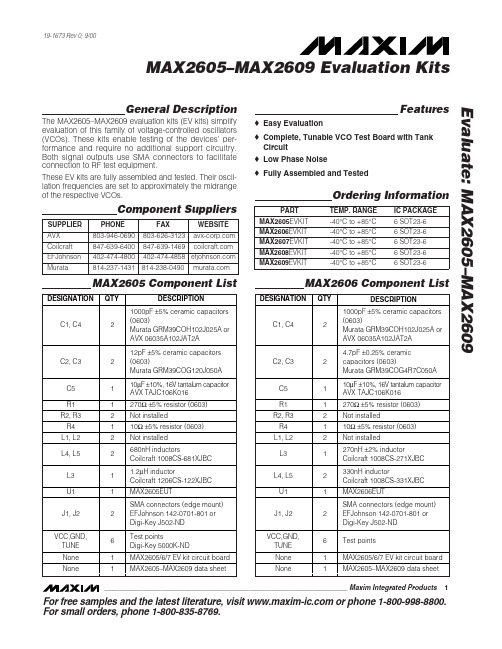
General DescriptionThe MAX2605–MAX2609 evaluation kits (EV kits) simplify evaluation of this family of voltage-controlled oscillators (VCOs). These kits enable testing of the devices’ per-formance and require no additional support circuitry.Both signal outputs use SMA connectors to facilitate connection to RF test equipment.These EV kits are fully assembled and tested. Their oscil-lation frequencies are set to approximately the midrange of the respective VCOs.Featureso Easy Evaluationo Complete, Tunable VCO Test Board with Tank Circuit o Low Phase Noiseo Fully Assembled and TestedEvaluate: MAX2605–MAX2609MAX2605–MAX2609 Evaluation Kits19-1673 Rev 0; 9/00Ordering InformationComponent SuppliersFor free samples and the latest literature, visit or phone 1-800-998-8800.For small orders, phone 1-800-835-8769.MAX2606 Component ListMAX2605 Component ListE v a l u a t e : M A X 2605–M A X 2609MAX2605–MAX2609 Evaluation Kits 2_______________________________________________________________________________________Quick StartThe MAX2605–MAX2609 evaluation kits are fully assembled and factory tested. Follow the instructions in the Connections a nd Setup section for proper device evaluation.Test Equipment Required•Low-noise power supplies (these are recommended for oscillator noise measurement). Noise or ripple will frequency-modulate the oscillator and cause spectral spreading. Batteries can be used in place of power supplies, if necessary.– Use a DC power supply capable of supplying +2.7V to +5.5V. Alternatively, use two or three 1.5V batteries.– Use a DC power supply capable of supplying +0.4V to +2.4V, continuously variable, for TUNE.Alternatively, use two 1.5V batteries with a resistive voltage divider or potentiometer.•An RF spectrum analyzer that covers the operating frequency range of the MAX2605–MAX2609• A 50Ωcoaxial cable with SMA connectors •An ammeter (optional)Connections and Setup1)Connect a DC supply (preset to +3V) to the V CC and GND terminals (through an ammeter, if desired) on the EV kit.2)Turn on the DC supply. If used, the ammeter readingMAX2607 Component ListMAX2608 Component ListEvaluate: MAX2605–MAX2609MAX2605–MAX2609 Evaluation Kits_______________________________________________________________________________________3approximates the typical operating current specified in the MAX2605–MAX2609 data sheet.3)Connect the VCO output (OUT+ or OUT-) to a spec-trum analyzer with a 50Ωcoaxial cable.4)Apply a positive variable DC voltage between 0.4V and 2.4V to TUNE.5)Check the tuning bandwidth on the spectrum analyz-er by varying the tuning voltage (+0.4V to +2.4V).Layout ConsiderationsThe EV kit PC board can serve as a guide for laying out a board using the MAX2605–MAX2609. Generally, the VCC pin on the PC board should have a decoupling capacitor placed close to the IC. This minimizes noisecoupling from the supply. Also, place the VCO as far away as possible from the noisy section of a larger sys-tem, such as a switching regulator or digital circuits.The VCO ’s performance is strongly dependent on the availability of the external tuning inductor. For best per-formance, use high-Q components and choose their val-ues carefully. To minimize the effects of parasitic ele-ments, which degrade circuit performance, place the tuning inductor and C BYP close to the VCO. For higher-frequency versions, include the parasitic PC board inductance and capacitance when calculating the oscillation frequency. In addition, remove the ground plane around and under the tuning inductor to minimize the effect of parasitic capacitance.Noise on TUNE translates into FM noise on the outputs;therefore, keep the trace between TUNE and the control circuitry as short as possible. If necessary, use an RC filter to further suppress noise, as done on the EV kits.E v a l u a t e : M A X 2605–M A X 2609MAX2605–MAX2609 Evaluation Kits 4_______________________________________________________________________________________Figure 2. MAX2608/MAX2609 EV Kits SchematicFigure 1. MAX2605/MAX2606/MAX2607 EV Kits SchematicEvaluate: MAX2605–MAX2609MAX2605–MAX2609 Evaluation Kits_______________________________________________________________________________________5Figure 3. MAX2605/MAX2606/MAX2607 EV Kits ComponentPlacement Guide—Top Silk ScreenFigure 4. MAX2608/MAX2609 EV Kits Component PlacementGuide—Top Silk ScreenFigure 5. MAX2605/MAX2606/MAX2607 EV Kits PC BoardLayout—Component SideFigure 6. MAX2608/MAX2609 EV Kits PC Board Layout—Component SideMa xim ca nnot a ssume responsibility for use of a ny circuitry other tha n circuitry entirely embodied in a Ma xim product. No circuit pa tent licenses a re implied. Maxim reserves the right to change the circuitry and specifications without notice at any time.6_____________________Maxim Integrated Products, 120 San Gabriel Drive, Sunnyvale, CA 94086 408-737-7600©2000 Maxim Integrated ProductsPrinted USAis a registered trademark of Maxim Integrated Products.E v a l u a t e : M A X 2605–M A X 2609MAX2605–MAX2609 Evaluation Kits Figure 7. MAX2605/MAX2606/MAX2607/MAX2608/MAX2609EV Kits PC Board Layout—Ground Plane。
- 1、下载文档前请自行甄别文档内容的完整性,平台不提供额外的编辑、内容补充、找答案等附加服务。
- 2、"仅部分预览"的文档,不可在线预览部分如存在完整性等问题,可反馈申请退款(可完整预览的文档不适用该条件!)。
- 3、如文档侵犯您的权益,请联系客服反馈,我们会尽快为您处理(人工客服工作时间:9:00-18:30)。
General DescriptionThe MAX6391/MAX6392 microprocessor (µP) supervisory circuits provide sequenced logic reset outputs for multi-component or dual-voltage systems. Each device can monitor two supply voltages and time-sequence two reset outputs to control the order in which system components are turned on and off. The MAX6391/MAX6392 increase system reliability and reduce circuit complexity and cost compared to separate ICs or discrete components.The MAX6391/MAX6392 monitor V CC as the master reset supply. Both RESET1and RESET2are asserted whenever V CC drops below the selected factory-fixed reset threshold voltage. RESET1remains asserted as long as V CC is below the threshold and deasserts 140ms (min) after V CC exceeds the thresholds.RESET IN2 is monitored as the secondary reset supply and is adjustable with an external resistive-divider net-work. RESET2is asserted whenever either V CC or RESET I N2 is below the selected thresholds. RESET2remains asserted 140ms (min) or a capacitor-adjustable time period after V CC and RESET I N2exceed their thresholds. RESET2is always deasserted after RESET1during system power-up and is always asserted before RESET1during power-down.The MAX6391 includes two internal pullup resistors for RESET1and RESET2(the open-drain outputs can be externally connected to the desired pullup voltages).The MAX6392 includes an active-low manual reset input (MR ) that asserts both RESET1(push-pull) and RESET2(open drain).The MAX6391/MAX6392 are available in small 8-pin SOT23 packages and are specified over the -40°C to +85°C extended temperature range.ApplicationsComputers ControllersCritical µP Power Monitoring Set-Top Boxes PrintersServers/Workstations Industrial Equipment Multivoltage MonitoringFeatureso Preset V CC Reset Threshold Voltages from 1.58V to 4.63V (master supply)o Customer-Adjustable RESET IN2 to Monitor Voltages Down to 625mV (secondary supply) o Fixed (140ms min) R E S E T 1Timeout o Fixed (140ms min) or Customer-Adjustable R E S E T 2Timeout Period o Guaranteed Reset Valid to V CC = 1V o Active-Low Open-Drain Outputs or Push-Pull/Open-Drain Combinationo Internal Open-Drain Pullup Resistors (for external V OH voltage connections)o Manual Reset Input (MAX6392 only)o Immune to Short Negative V CC Transients o 15µA Typical Supply Current o Few External Components o Small 8-Pin SOT23 PackageMAX6391/MAX6392Dual-Voltage µP Supervisory Circuitswith Sequenced Reset Outputs________________________________________________________________Maxim Integrated Products1Pin ConfigurationsOrdering Information19-2210; Rev 1; 10/02*Insert the desired suffix (see Selector Guide) into the blanks to complete the part number. The MAX6391/MAX6392 require a 2.5k minimum order increment and are available in tape-and-reel only. Samples are typically available for standard versions (see Selector Guide for standard versions). Contact factory for availability.For pricing, delivery, and ordering information,please contact Maxim/Dallas Direct!at 1-888-629-4642, or visit Maxim’s website at .Typical Operating Circuit appears at end of data sheet.M A X 6391/M A X 6392Dual-Voltage µP Supervisory Circuits with Sequenced Reset Outputs 2_______________________________________________________________________________________ABSOLUTE MAXIMUM RATINGSELECTRICAL CHARACTERISTICSStresses beyond those listed under “Absolute Maximum Ratings” may cause permanent damage to the device. These are stress ratings only, and functional operation of the device at these or any other conditions beyond those indicated in the operational sections of the specifications is not implied. Exposure to absolute maximum rating conditions for extended periods may affect device reliability.V CC to GND...........................................................-0.3V to +6.0V RESET1(MAX6392), RESET IN2, CSRT,MR to GND..............................................-0.3V to (V CC + 0.3V)RESET1(MAX6391), RESET2, R1, R2 to GND......-0.3V to +6.0V Input Current (V CC , GND, CSRT, R1, R2, MR ).................±20mA Output Current (RESET1, RESET2)..................................±20mA Continuous Power Dissipation (T A = +70°C)8-Pin SOT23 (derate 5.26mW/°C above +70°C)...........421mWOperating Temperature Range ...........................-40°C to +85°C Junction Temperature......................................................+150°C Storage Temperature Range.............................-65°C to +150°C Lead Temperature (soldering, 10s).................................+300°CMAX6391/MAX6392Dual-Voltage µP Supervisory Circuitswith Sequenced Reset Outputs_______________________________________________________________________________________3ELECTRICAL CHARACTERISTICS (continued)(V CC = 1.2V to 5.5V, T A = T MIN to T MAX , unless otherwise specified. Typical values are at V CC = +5V and T A = +25°C.) (Note 1)Note 2:RESET2asserts before RESET1when V CC goes below the threshold for all supply voltage and temperature ranges.Note 3:CSRT must be connected to either V CC (for fixed RESET2timeout period) or an external capacitor (for user-adjustable RESET2timeout period).M A X 6391/M A X 6392Dual-Voltage µP Supervisory Circuits with Sequenced Reset Outputs 4_______________________________________________________________________________________Typical Operating Characteristics(V CC = +5V, T A = +25°C, unless otherwise noted.)10.811.011.411.211.611.8-4010-15356085RESET2 TO RESET1 DELAYvs. TEMPERATURETEMPERATURE (°C)D E L A Y (µs )200225250275300-40-1510356085RESET1 TIMEOUT PERIOD vs. TEMPERATUREM A X 6391 t o c 05TEMPERATURE (°C)T I M E O U T D E L A Y (m s )2.502.753.003.253.50-40-1510356085RESET1 TO RESET2 TIMEOUT PERIOD vs. TEMPERATURE (CSRT = 1500pF)M A X 6391 t o c 06TEMPERATURE (°C)T I M E O U T D E L A Y (m s )200225250275300-40-1510356085RESET1 TO RESET2 TIMEOUT PERIOD vs. TEMPERATURE (CSRT TIED TO V CC )M A X 6391 t o c 07TEMPERATURE (°C)T I M E O U T D E L A Y (m s )102040305060MAXIMUM TRANSIENT DURATION vs. RESET COMPARATOR OVERDRIVEOVERDRIVE (mV)M A X I M U M T R A N S I E N T D U R A T I O N (µs )11001010001716151413-4010-15356085SUPPLY CURRENT vs. TEMPERATUREM A X 6391 t o c 01TEMPERATURE (°C)S U P P L Y C U R R E N T (µA )202122232425262728-40-1510356085V CC FALLING TO RESET1 DELAY VS.TEMPERATUREM A X 6391 t o c 02TEMPERATURE (°C)D E L A Y (µs )91011121314151617-40-1510356085V CC FALLING TO RESET2 DELAYvs. TEMPERATUREM A X 6391 t o c 03TEMPERATURE (°C)D E L A Y (µs )MAX6391/MAX6392Dual-Voltage µP Supervisory Circuitswith Sequenced Reset Outputs_______________________________________________________________________________________5Detailed DescriptionEach device includes a pair of voltage monitors with sequenced reset outputs. The first block monitors V CC only (RESET1output is independent of the RESET IN2monitor). It asserts a reset signal (LOW) whenever V CC is below the preset voltage threshold. RESET1remains asserted for at least 140ms after V CC rises above the reset threshold. RESET1timing is internally set in each device. V CC voltage thresholds are available from 1.57V to 4.63V. I n all cases V CC acts as the master supply (all resets are asserted when V CC goes below its selected threshold). The V CC input also acts as the device power supply.The second block monitors both RESET IN2 and V CC . It asserts a reset signal (LOW) whenever RESET I N2 is below the 625mV threshold or V CC is below its reset threshold. RESET2remains asserted for a fixed 140ms(min) or a user-adjustable time period after RESET IN2rises above the 625mV reset threshold and RESET1is deasserted. Resets are guaranteed valid for V CC down to 1V.The timing diagram in Figure 2 shows the reset timing characteristics of the MAX6391/MAX6392. As shown in Figure 2, RESET1deasserts 140ms (min) (t RP1) after V CC exceeds the reset threshold. RESET2deasserts t RP2(140ms minimum or a user-adjustable timeout peri-od) after RESET I N2 exceeds 625mV and RESET1is deasserted. When RESET I N2 drops below 625mV while V CC is above the reset threshold, RESET2asserts within 10µs typ. RESET1is unaffected when this hap-pens. When V CC falls below V TH1, RESET2always asserts before RESET1(t RD2< t RD1).M A X 6391/M A X 6392Dual-Voltage µP Supervisory Circuits with Sequenced Reset Outputs 6_______________________________________________________________________________________Figure 1. Functional DiagramFigure 2. Timing DiagramMAX6391/MAX6392Dual-Voltage µP Supervisory Circuitswith Sequenced Reset Outputs_______________________________________________________________________________________7Applications InformationSelecting the Reset Timeout CapacitorThe RESET2delay may be adjusted by the user with an external capacitor connected from the CSRT pin to ground. The MAX6391 includes a 600nA current source that is switched to C CSRT to create a voltage ramp. The voltage ramp is compared to the internal 1.25V refer-ence to set the RESET2delay period. The period is cal-culated by:∆t = C ✕∆V/Iwhere ∆V = 1.25V, I = 600nA, and C is the external capacitor.Simplifying,t RP = 2.08 ✕106s / F ✕C CSRT For C CSRT = 1500pF, t RP = 3.1msA fixed internal 140ms (min) reset delay time for RESET2may be chosen by connecting the CSRT pin to V CC . The V CC to CSRT connection disables the voltage ramp and enables a separate fixed delay counterchain. The MAX6391 internally determines the CSRT connection and provides the proper timing setup.In all cases, RESET IN2 acts as the slave supply. V CC can assert the RESET2output but RESET IN2 will have no effect on the RESET1output.Monitoring Voltages Other Than V CCAn external resistive-divider network is required at RESET IN2 for most applications. The divider resistors,R3 and R4, may be calculated by the following formula:V RST = V TH2✕(R3 + R4)/R4where V TH2= 625mV (internal reference voltage) and V RST is the desired reset threshold voltage. R4 may be set to a conveniently high value (500k Ωfor example, to minimize current consumption) and the equation may be solved for R3 by:R3 = R4 ✕(V RST /V TH2- 1)For single-supply operations requiring two reset out-puts (RESET1before RESET2), connect RESET I N2directly to V CC and adjust RESET2timeout delay with C CRST as desired.Pullup ResistorsThe MAX6391 includes open-drain outputs for both RESET1and RESET2. Two internal resistors, R1 and R2, of 47k Ωeach are provided with internal connec-tions to RESET1and RESET2. These resistors may be connected to the appropriate external voltage for inde-pendent V OH drive with no additional component requirements.The MAX6392 includes a manual reset option, MR , that replaces the R1 pullup resistor. The active-low manual reset input forces both RESET1and RESET2low.RESET2is driven active before RESET1in all cases (10µs typ). The resets follow standard reset timing specifications after the manual reset is released. The manual reset is internally pulled up to V CC through a 47k Ωresistor.Negative-Going V CC TransientsIn addition to issuing a reset to the µP during power-up,power-down, and brownout conditions, these devices are relatively immune to short-duration, negative-going V CC or RESET I N2 transients (glitches). The Typical Operating Characteristics show the Maximum Transient Duration vs. Reset Comparator Overdrive graph. The graph shows the maximum pulse width that a negative-going V CC transient may typically have without issuing a reset signal. As the amplitude of the transient increas-es, the maximum allowable pulse width decreases.M A X 6391/M A X 6392Chip InformationTRANSISTOR COUNT: 810PROCESS: BiCMOSDual-Voltage µP Supervisory Circuits with Sequenced Reset Outputs 8_______________________________________________________________________________________Typical Operating CircuitMAX6391/MAX6392Dual-Voltage µP Supervisory Circuitswith Sequenced Reset OutputsMaxim cannot assume responsib ility for use of any circuitry other than circuitry entirely emb odied in a Maxim product. No circuit patent licenses are implied. Maxim reserves the right to change the circuitry and specifications without notice at any time.Maxim Integrated Products, 120 San Gabriel Drive, Sunnyvale, CA 94086 408-737-7600 _____________________9©2002 Maxim Integrated ProductsPrinted USAis a registered trademark of Maxim Integrated Products.Package Information(The package drawing(s) in this data sheet may not reflect the most current specifications. For the latest package outline information go to /packages .)。