SNC549中文资料
运算放大器(AD549)应用中文技术资料

极低偏置电流运算放大器AD5491 概述AD549是具有极低输入偏置电流的单片电路静电计型运算放大器。
为达到高精度的目的,输入偏置电压和输入偏置电压漂移均通过激光调节。
这种极低输入电流性能由ADI公司专有的topgate工艺技术完成。
该技术可以制造与具有极低输入电流的JFET并与双极性电路隔离的集成运放。
输入级具有1015Ω的共模阻抗,其输入电流与共模电压无关。
AD549适用于低输入电流和低输入偏置电压的场合。
它特别适合用作各种电流输出的传感器,如光电二极管、光电倍增管以及氧气传感器等的前置放大器。
该产品也可用作精密积分器或低衰减采样保持器。
AD549的封装与标准FET和静电计运算放大器兼容,因此用户花少量成本即可对系统升级,提高已有系统的性能。
AD549有TO-99密封封装。
金属外壳与8管脚相连,使得金属外壳与同样电压的输入终端独立连接,达到降低外壳泄漏的目的。
AD549具有四种性能等级。
其中J、K和L型号的温度范围是0℃到70℃。
S型号专用于军事,其温度范围:-55℃到125℃。
AD549的输入电流在整个共模输入电压范围内都得到保证,其输入失调电压和漂移由激光分别调节到0.25mV和5μV/℃(AD549K);1mV和20μV/℃(AD549J)。
700μA的最大静态电流使输入电流和偏置电压的热效应降到最低。
模拟性能包括1MHz的均匀增益带宽和3V/μs的压摆率。
当输入为10V时,建立时间是5μs 到0.01%。
2 AD549的引脚及特性参数图一所示是AD549的引脚图,表一所示是其特性参数。
图一AD549引脚图表一AD549的主要特性nV/ nV/ nV/ nV/3 AD549的工作原理3.1 最小化输入电流AD549具有很小的输入电流和失调电压。
在实际应用中应谨慎考虑如何使用放大器可以减小输入电流。
为减小输入电流,该放大器的工作温度应尽可能低。
像其他JFET输入放大器一样,AD549的输入电流对芯片温度很敏感,上升斜率因子为每10℃的2.3。
基于TLC549的温度采集系统
基于TLC549的温度采集系统摘要关键词:温度采集、AD转换、AT89C51、四段七位数码管静态显示本次课程设计主要是用AD590、AT89C51、TLC549和四段七位静态数码管设计一个简易温度采集系统。
用AD590采集温度信号,输出一个模拟电压信号,输入到TLC549模拟信号输入端,用单片机控制TLC549转换,转换成的数字信号利用单片机存入累加器A中,在累加器A中对该数字信号进行操作,转换成十进制后,经过74LS164将段码送到四位七位数码管中,并显示该十进制数(带小数点),即温度值。
该系统的主要功能是采集一个温度信号,经过一系列转换后,将该温度显示出来,采集的温度范围为0到67度,误差在5%左右,显示的最大值为63.75度。
在编写程序之前,首先要了解实验台上各各模块的电路图及原理,然后再学会用程序控制它。
用Keil C软件装载、下载、编译程序,并与伟福仿真器联用调试,逐步改正错误,最后实现实验要求。
然后再改进程序,添加注释,使程序条理清晰,明白易懂。
最后的最后,答辩,写报告。
目录第一章系统方案 (3)1.1设计内容 (3)1.2设计要求 (3)1.3设备及工作环境 (3)第二章理论分析与计算 (4)2.1设计思路 (4)2.2硬件结构及原理电路图 (4)2.3重要硬件元件功效阐明 (6)第三章程序设计 (7)3.1分析论证 (7)3.2程序流程图 (8)3.3程序清单: (9)第四章结果分析 (15)第五章总结 (15)参考文献 (16)第一章系统方案1. 1设计内容利用温度传感器AD590采集温度信号,并调理放大采集到的电压信号,用TLC549进行电压转换,实现温度采集,并将采集温度显示出来。
1. 2设计要求(1)在综合单片机实验台的硬件结构上编写软件完成设计。
(2)程序的首地址应使目标机可以直接运行,即从0000H开端。
(3)四位显示器数码管从右到左分辨显示,显示xx.xx(最高温度为63.75度)。
芯片TLC549介绍(中文的)
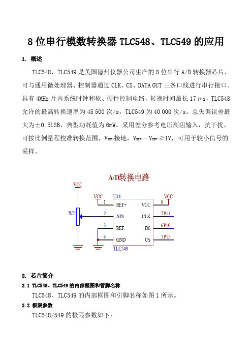
8位串行模数转换器TLC548、TLC549的应用1. 概述TLC548,TLC549是美国德州仪器公司生产的8位串行A/D转换器芯片,可与通用微处理器、控制器通过CLK、CS、DATA OUT三条口线进行串行接口。
具有4MHz片内系统时钟和软、硬件控制电路,转换时间最长17μs,TLC548允许的最高转换速率为45 500次/s,TLC549为40 000次/s。
总失调误差最大为±0.5LSB,典型功耗值为6mW。
采用差分参考电压高阻输入,抗干扰,可按比例量程校准转换范围,V REF-接地,V REF+-V REF-≥1V,可用于较小信号的采样。
2. 芯片简介2.1 TLC548、TLC549的内部框图和管脚名称TLC548、TLC549的内部框图和引脚名称如图1所示。
2.2 极限参数TLC548/549的极限参数如下:●电源电压:6.5V;●输入电压范围:0.3V~V CC+0.3V;●输出电压范围:0.3V~V CC+0.3V;●峰值输入电流(任一输入端):±10mA;●总峰值输入电流(所有输入端):±30mA;●工作温度:TLC548C、TLC549C:0℃~70℃TLC548I、TLC549I:-40℃~85℃TLC548M、TLC549M:-55℃~125℃3. 工作原理TLC548、TLC549均有片内系统时钟,该时钟与I/O CLOCK是独立工作的,无须特殊的速度或相位匹配。
其工作时序如图2所示。
当CS为高时,数据输出(DATA OUT)端处于高阻状态,此时I/O CLOCK 不起作用。
这种CS控制作用允许在同时使用多片TLC548、TLC549时,共用I/O CLOCK,以减少多路(片)A/D并用时的I/O控制端口。
一组通常的控制时序为:(1)将CS置低。
内部电路在测得CS下降沿后,再等待两个内部时钟上升沿和一个下降沿后,然后确认这一变化,最后自动将前一次转换结果的最高位(D7)位输出到DATA OUT端上。
LC549中文资料

LC549/LV549/LD549 DATA SHEETHigh Power Class BOutput StageFEATURES•40dB of electrical gain• 1.0 to 1.6 VDC supply operating range •current trim capability (R T )•high efficiency class B output stage•may be used with a linear or compression preamplfier STANDARD PACKAGING •8 pin MICROpac (LC549)•8 pin MINIpac•8 pin PLID ® (LC549, LD549)•Chip (47 x 40 mils) (LC549, LD549)DESCRIPTIONThe LC/LV/LD549 is an 8 pin, low voltage, push-pull audio frequency output stage amplifier with a single unbalanced input. The circuit utilizes two internal negative feedback loops to stabilize the DC operating point for temperature stability and to linearize the transfer function over a wide dynamic range. The circuit operates near ideal class B conditions resulting in low distortion and very low quiescent current, required for extended battery life.The LC549, LV549 and LD549 differ in only one respect;the LV549 and LD549 are selected devices which are capable of delivering from 10 mA to 41 mA and from 36 mA to 75 mA of output current respectively. These values are the maximum current drawn with both output stage transistors in saturation. Thus the LD549 is capable of producing a high output in a low impedance load, the LV549 is selected to have lower peak currents, extending the life of the battery.U.S. Patent No. 4,085,382Patented in other countriesBLOCK DIAGRAMR T V BINPUTDEC 1 DEC 2GNDGENNUM CORPORATION P.O. Box 489, Stn A, Burlington, Ontario, Canada L7R 3Y3 tel. (905) 632-2996 fax: (905) 632-5946Japan Branch: A-302 Miyamae Village, 2-10-42 Miyamae, Suginami-ku Tokyo 168, Japan tel. (03) 3334-7700 fax: (03) 3247-8839Document No. 500 - 25 - 09Revision Date: January 20012500 - 25 - 09SEQUENCE CONDITIONS COMMENTS 1 Power Supply Off 2S1Closed Removes V IN3S2 / S3Closed Discharges C2 and C34 S1Open Applies V IN (V IN level is determined from Gain Test) 5S2 / S3Open Removes short from C2 and C36Power SupplyOn7Gain must be within specification, within 3 seconds after power supply is turned onABSOLUTE MAXIMUM RATINGSPARAMETER VALUE & UNITSSupply Voltage 3 VDC Power dissipation 60 mWOperating Temperature -10 to + 40 °C Storage Temperature-20 to + 70 °CPIN CONNECTIONR T I/P DEC2V B GNDOUT1OUT2ELECTRICAL CHARACTERISTICSConditions: Temperature 25 o C, Supply Voltage V B = 1.3 VDCAll switches and parameters remain as shown in test circuit unless stated in condition columnPARAMETER SYMBOL CONDITION MIN TYP MAX UNITSGainA CL V OUT = 0.707 V RMS384042dB Quiescent CurrentI AMP 100-400µA I TRANS 170-370µA I TOT-500770µAMaximum Drive CurrentV1 = 0V (S2, S3 closed)V4 = 0V LC549103575mA LV54910-41mA LD549365075mA Input Impedance182736k ΩTotal Harmonic Distortion & NoiseTHDV OUT = 0.707 V RMS -0.5-%V OUT = 1.3 V RMS- 2.5 5.2%Input Referred Noise IRN NFB 0.2 to 10 kHz at 12 dB/oct (S1 closed)- 1.2 2.5µV Start Up Time--3secSTART-UP TIME TEST (Refer to Test Circuit)3500 - 25 - 09Fig. 1 Test CircuitAll resistors in ohms, all capacitors in farads unless otherwise stated U.S. Patent No. 4,085,382 - Patented in other countriesFig. 2 Equivalent CircuitV = R T = 600Ω1kHzAll resistors in ohms, all capacitors in µF unless otherwise statedGain = 20 Log 10( ) +40 dB VOUT VIN=∞4500 - 25 - 09V B=1.3VDCMICTEMPERATURE °CFig. 4 Volume Gain vs Battery VoltageFig. 5 Quiescent Current vs Battery VoltageFig. 6 Quiescent Current vs TemperatureFig. 7 Gain vs Temperature-20 -10 0 10 20 30 40 50 60 7041.040.239.438.637.837.0464442403836A V (dB )V B (V)V B (V)I Q (µA )I Q (µA )-20 -10 0 10 20 30 40 50 60 70TEMPERATURE (°C)A V (dB )8007006005004003000.9 1.0 1.1 1.2 1.3 1.4 1.5 1.6 1.7 1.85325245165085004920.9 1.0 1.1 1.2 1.3 1.4 1.5 1.6 1.7 1.85500 - 25 - 09R E L A T I V E V O L T A G E G A I N (d B )Gennum Corporation assumes no responsibility for the use of any circuits described herein and makes no representations that they are free from patent infringement.© Copyright January 1981 Gennum Corporation. All rights reserved. Printed in Canada.P O W E R O U T P U T (m V )I Q (µA )A V (d B)0 4 8 12 16 20 24 260.01 0.1 1.0 10 10012108642LDLC-0 200 400 600 800 1k41403938373640.440.240.039.839.6550500450400350300250200LOAD R L (Ω)FREQUENCY (kHZ)Fig. 9 Voltage Gain vs FrequencyFig. 8 Power Output vs Load Resistance at 7% Distortion R B = 0Ω1 10 100 1KSUPPLY VOLTAGE (V)Fig. 11 Voltage Gain vs Battery ResistanceFig. 10 Quiescent Current vs Current Trim Resistor R T(k Ω)DOCUMENT IDENTIFICATIONPRODUCT PROPOSALThis data has been compiled for market investigation purposes only, and does not constitute an offer for sale.ADVANCE INFORMATION NOTEThe product is in a development phase and specifications are subject to change without notice. Gennum reserves the right to remove the product at any time. Listing the product does not constitute an offer for sale.PRELIMINARY DATA SHEETThe product is in preproduction phase and specifications are subject to change without notice.DATA SHEETThe product is in production. Gennum reserves the right to make changes at any time to improve reliability, function or design, in order to provide the best product possible.。
目前常用的AD芯片(TI公司)
⽬前常⽤的AD芯⽚(TI公司)⽬前AD/DA的常⽤芯⽚介绍:TI公司AD/DA器件:1)TLC548/549TLC548和TLC549是以8位开关电容逐次逼近A/D转换器为基础⽽构造的CMOSA/D转换器。
它们设计成能通过3态数据输出与微处理器或外围设备串⾏接⼝。
TLC548和TLC549仅⽤输⼊/输出时钟和芯⽚选择输⼊作数据控制。
TLC548的最⾼I/OCLOCK 输⼊频率为2.048MHz,⽽TLC549的I/OCLOCK输⼊频率最⾼可达1.1MHz。
TLC548和TLC549的使⽤与较复杂的TLC540和TLC541⾮常相似;不过,TLC548和TLC549提供了⽚内系统时钟,它通常⼯作在4MHz且不需要外部元件。
⽚内系统时钟使内部器件的操作独⽴于串⾏输⼊/输出端的时序并允许TLC548和TLC549象许多软件和硬件所要求的那样⼯作。
I/OCLOCK和内部系统时钟⼀起可以实现⾼速数据传送,对于TLC548为每秒45,500次转换,对于TLC549为每秒40,000次的转换速度。
TLC548和TLC549的其他特点包括通⽤控制逻辑,可⾃动⼯作或在微处理器控制下⼯作的⽚内采样-保持电路,具有差分⾼阻抗基准电压输⼊端,易于实现⽐率转换(ratiometricconversion).定标(scaling)以及与逻辑和电源噪声隔离的电路。
整个开关电容逐次逼近转换器电路的设计允许在⼩于17µs的时间内以最⼤总误差为±0.5最低有效位(LSB)的精度实现转换。
2)TLV5616TLV5616是⼀个12位电压输出数模转换器(DAC),带有灵活的4线串⾏接⼝,可以⽆缝连接TMS320.SPI.QSPI和Microwire串⾏⼝。
数字电源和模拟电源分别供电,电压范围2.7~5.5V。
输出缓冲是2倍增益rail-to-rail输出放⼤器,输出放⼤器是AB类以提⾼稳定性和减少建⽴时间。
rail-to-rail输出和关电⽅式⾮常适宜单电源。
TLC1549中文资料

TLC1549中文资料2009-08-14 21:52TLC1549C , TLC1549I , TLC1549M 10位模拟数字转换器(A/D)串行控制#10位分辨率A / D转换器#固有的采样保持#未经调整的总误差........± 1 LSB的最大值#片上系统时钟#终端兼容TLC549和TLV1549#CMOS工艺描述该TLC1549C , TLC1549I ,并TLC1549M 有10位,开关电容,successiveapproximation 模拟数字转换器。
这些器件有两个数字输入和一个3态输出[片选( CS )的,输入输出时钟( I / O时钟)和数据输出(数据) ]的提供三线接口,串口主机处理器。
该采样保持功能是自动的。
那个转换纳入这些设备的特点差分高阻抗基准投入便利比率转换,缩放,和隔离模拟电路的逻辑和供应噪音。
开关电容设计,让lowerror 转换的整个经营自由空气温度范围。
该TLC1549C运作的特点是从0 ° C至70 °角该TLC1549I的特点是操作从-40 ° C 至85 ° C该TLC1549M特点是操作,在整个军事温度范围 -55 ℃至125 ℃之间。
管脚说明:ANALOG IN (2):模拟信号输入。
驱动源阻抗应该是3月1日千瓦。
外部驱动源的模拟,应该有一个电流能力。
一十毫安。
CS (5):芯片选择。
高向低过渡的政务司司长重置内部计数器和控制,使数据和I / O时钟内最大的一个设置时间加上两个属于边缘内部系统时钟。
低到高过渡禁用I / O时钟设置时间内下降的边缘加两国的内部系统时钟。
DATA OUT (6):这3态串行输出的A / D转换结果是在高阻抗状态时,政务司司长高,积极当政务司司长低。
以有效的芯片选择,数据是从高阻抗状态,并驱车前往相应的逻辑电平的最高有效位价值先前的转换结果。
下一个下降沿的I / O 时钟驱动器DATAOUT的逻辑水平相应的下一个最重要的一点,其余位转移,以便与LSB的出现在第九届下降沿的I / O时钟。
芯片TLC549,TLC548介绍_中文的_

8位串行模数转换器TLC548、TLC549的应用1. 概述TLC548,TLC549是美国德州仪器公司生产的8位串行A/D转换器芯片,可与通用微处理器、控制器通过CLK、CS、DATA OUT三条口线进行串行接口。
具有4MHz片内系统时钟和软、硬件控制电路,转换时间最长17μs,TLC548允许的最高转换速率为45 500次/s,TLC549为40 000次/s。
总失调误差最大为±0.5LSB,典型功耗值为6mW。
采用差分参考电压高阻输入,抗干扰,可按比例量程校准转换范围,V REF-接地,V REF+-V REF-≥1V,可用于较小信号的采样。
2. 芯片简介2.1 TLC548、TLC549的内部框图和管脚名称TLC548、TLC549的内部框图和引脚名称如图1所示。
2.2 极限参数TLC548/549的极限参数如下:●电源电压:6.5V;●输入电压范围:0.3V~V CC+0.3V;●输出电压范围:0.3V~V CC+0.3V;●峰值输入电流(任一输入端):±10mA;●总峰值输入电流(所有输入端):±30mA;●工作温度:TLC548C、TLC549C:0℃~70℃TLC548I、TLC549I:-40℃~85℃TLC548M、TLC549M:-55℃~125℃3. 工作原理TLC548、TLC549均有片内系统时钟,该时钟与I/O CLOCK是独立工作的,无须特殊的速度或相位匹配。
其工作时序如图2所示。
当CS为高时,数据输出(DATA OUT)端处于高阻状态,此时I/O CLOCK 不起作用。
这种CS控制作用允许在同时使用多片TLC548、TLC549时,共用I/O CLOCK,以减少多路(片)A/D并用时的I/O控制端口。
一组通常的控制时序为:(1)将CS置低。
内部电路在测得CS下降沿后,再等待两个内部时钟上升沿和一个下降沿后,然后确认这一变化,最后自动将前一次转换结果的最高位(D7)位输出到DATA OUT端上。
EN549中文版
英国标准规范于燃气器具、设备密封件和膜片用橡胶材料欧洲标准EN549 :1994年以来的英国标准未经BSI允许不得拷贝此英国标准责任委员会此英国标准委托GSE/22技术委员会进行编辑,燃气具的安全与控制如下所诉:控制器制造商协会(TAMCA(BEAMA有限公司英国电器制造厂商协会));英国燃气公司(英国)贸工部(消费者安全协会,加利福利亚分部)液化石油气协会英国燃气工业协会修订后出版发行委员会指导编辑,标准委员会权威发行,于1995年5月15日实施。
此后BSI条款涉及工作标准:GSE/22 标准委员会92/82881 DC 征求意见稿前言此英国标准委托GSE/22技术委员会进行编辑,EN 549:1994为英文版,燃气器具、设备密封件和膜片用橡胶材料,由欧洲标准化委员会(CEN)出版。
此标准替代BS 6505。
EN549是由英国积极参加国际讨论后所出版。
互相参照出版物对应英国标准BS(英国国家标准)903 橡胶物性测试ISO48 A26. 硬度确定ISO188 A19. 耐热性与加速老化试验ISO247 BS 7164 原材料与硫化橡胶的化学测试5. 灰分含量的确定方法BS 903 橡胶物性ISO471 A35. 试验片的测试时间、温度、湿度的调节ISO815 A6. 压缩变形的环境、高低温的确定方法ISO1400 A26. 硬度确定ISO1407 BS 1673 橡胶原材料及未加硫复合橡胶的测试方法2.橡胶原材料的化学分析BS 903 橡胶物性测试ISO1431-1 A43. 抗臭氧开裂性确定方法(静态应变测试)ISO1817:1985 A16.1987 液体中效果确定BS 903 橡胶物性测试ISO4648 A38. 用于测试的试验片及产品的尺寸确定方法ISO4650 BS 4181 橡胶红外光谱鉴定1.碳化氢、氯丁二烯、丁腈及氯磺化聚乙烯橡胶的确定方法遵守英国标准,本身并不赋予法律义务的豁免权。
- 1、下载文档前请自行甄别文档内容的完整性,平台不提供额外的编辑、内容补充、找答案等附加服务。
- 2、"仅部分预览"的文档,不可在线预览部分如存在完整性等问题,可反馈申请退款(可完整预览的文档不适用该条件!)。
- 3、如文档侵犯您的权益,请联系客服反馈,我们会尽快为您处理(人工客服工作时间:9:00-18:30)。
1 INTRODUCTIONSNC549 is a two-channel voice synthesizer IC with PWM direct drive circuit. It built-in a 4-bit tiny controller with one 4-bit input port, two 4-bit output ports and three 4-bit I/O ports. By programming through the tiny controller in SNC549, user’s varied applications including voice section combination, key trigger arrangement, output control, and other logic functions can be easily implemented.2 FEATURESSingle power supply 2.4V – 5.5V16 seconds voice capacity are provided(@6KHZ sample rate)Built in a 4-bit tiny controllerOne 4-bit input port, two 4-bit output ports and three 4-bit I/O ports are provided 128*4 bits RAM are provided52K*10 ROM size are provided for voice data and programMaximum 16k program ROM is providedReadable ROM code dataIR carrier signal is providedBuilt in a high quality speech synthesizerAdaptive playing speed from 2.5k-20kHz is providedTwo independent voice channels (Channel 1 + Channel 2→Buo1,Buo2)Built in a PWM Direct Drive circuit and a fixed current D/A outputSystem clock : 2MHzLow Power Reset3 Block Diagram4 PIN ASSIGNMENTSymbol I/O Function DescriptionP13 ~ P10 I Bit3 ~ Bit0 of Input port 1P23 ~ P20 I/O Bit3 ~ Bit0 of I/O port 2P33 ~ P30 I/O Bit3 ~ Bit0 of I/O port 3P43 ~ P40 O Bit3 ~ Bit0 of Output port 4P53 ~ P50 O Bit3 ~ Bit0 of Output port 5P63 ~ P60 I/O Bit3 ~ Bit0 of I/O port 6VDD P Positive power supplyGND P Negative power supplyRST I Reset pin (active high)OSC O Oscillator / Crystal OutOutput of PWM or DA outputPositiveBUO1/VO OBUO2 O Negative Output of PWMTwo Channel Direct Drive Speech Controller5 FUNCTION DESCRIPTIONS 5.1. OscillatorSNC549 accept RC type oscillator for system clock. The typical circuit diagram for oscillator is listed as follow.rOSCVCCRC Oscillator5.2. ROMSNC549 contains substantial 52K words (10-bit) internal ROM. Program, voices and other data are shared with this same 52K words ROM.5.3. RAMSNC549 contains 128 nibbles RAM. The 128 nibbles RAM are divided into eight pages (page 0 to page 7, 16 nibble RAM on each page). In our programming structure, users can easily define and locate RAM page in the program. For instance, users can use the instructions, PAGEn (n=0 to 7) to switch and indicate the RAM page. Besides, users can use direct mode, M0 ~ M15 in the data transfer type instructions, to access all 16 nibbles of each page.5.4. Power Down Mode“End” instruction will power down SNC549 and enable IC to consume fewer current for power saving. (<3uA @VDD=3V and <5uA @VDD=5V) Please be aware that when the power down mode is activated in SNC549, any valid data transition (L H or H L) occurring on any input port (P1) or IO ports (P2, P3 and P6) will lead SNC549 back to normal operation mode.5.5. Sampling Rate Counters2 independent sampling rate counters are dedicated to 2 individual voice channels to be able to play diverse voices at different sample playing rates. The playing rate can be adaptively set up among from the wide ranges of 2.5KHz to 20KHz. This feature makes voice close to its original source and yield the better voice quality.Two Channel Direct Drive Speech Controller5.6. I/O PortsP1 is a 4-bit input port, P2/P3/P6 are three 4-bit I/O ports and P4/P5 are two 4-bit output ports. Any bit of P2, P3 and P6 can be programmed as either input or output port individually. Any valid data transition (H L or L H) of P1, P2, P3 and P6 can reactivate the chip when the chip is in power-down mode.Input Port Configuration (P10~P13)I/O Port Configuration (P20~P23, P30~P33, P60~P63)Two Channel Direct Drive Speech ControllerOutput Port Configuration (P40~P43, P50~P53)Note: All weak N-MOS’s can serve as pull-low resistors.5.7. IR FunctionP33 can be modulated with 38.5KHz square wave before sent out to P33 pin. The IR signal can be achieved by this modulated signal.5.8. DAC & PWMSNC549 is an advanced chip to be designed having two optimal methods to play out the voices. One is DAC and the other is PWM. Upon user’s applications, user can select either DAC or PWM in his design. Please be aware that only one method can be activated at a time.DAC: A 7-bit current type digital-to-analog converter is built-in SNC549. The relationship between input digital data and output analog current signal is listed in the following table. Also, the recommended application circuit is illustrated as follows.Two Channel Direct Drive Speech ControllerInput data Typical value of output current (mA)0 01 3/127…N n*(3/127)…127 3DAC outputPWM: A PWM (pulse width modulation) circuit is built-in SNC549. PWM can convert input digital data into pulse trains with suitable different pulse width. The maximum resolution of PWM is 7 bits. Two huge output stage circuits are designed in SNC549. With this advanced circuit, the chip is capable of driving speaker directly without external transistors. The recommended application circuit is illustrated as follows.PWM OutputTwo Channel Direct Drive Speech Controller 6 ABSOLUTE MAXIMUM RATINGItems Symbol Min Max Unit.Supply Voltage V DD-V -0.3 6.0 VInput Voltage V IN V SS-0.3 V DD+0.3 VOperating Temperature T OP 0 55.0 o CStorage Temperature T STG -55.0 125.0 o C7 ELECTRICAL CHARACTERISTICSItem Sym. Min. Typ. Max. Unit Condition Operating Voltage V DD 2.4 3.0 5.5 VStandby current I SBY - 2.05.0 - u A V DD=3V , no loadV DD=4.5V, no loadOperating Current I OPR - 300700 - u A V DD=3V , no loadV DD=4.5V, no loadInput current ofP1, P2, P3, P6I IH - 3.0 10.0 u A V DD=3V,V IN=3VDrive current ofP2, P3, P4, P5, P6I OD- 4 - m A V DD=3V,V O=2.4VSink Current ofP2, P3, P4, P5, P6I OS- 6 - m A V DD=3V,V O=0.4VDrive current ofP2, P3, P4, P5, P6I OD- 5 - m A V DD=4.5V,V O=3.9VSink Current ofP2, P3, P4, P5, P6I OS- 9 - m A V DD=4.5V,V O=0.4V Drive current of Buo1 I OD 100 120 - m A VDD=3V,Buo1=1.5V Sink Current of Buo1 I OS 100 120 - m A VDD=3V,Buo1=1.5V Drive Current of Buo2 I OD 100 120 - m A VDD=3V,Buo2=1.5V Sink Current of Buo2 I OS 100 120 - m A VDD=3V,Buo2=1.5V Oscillation Freq. F OSC - 2.0 - MHzV DD=3VIR Carrier Frequency Fir - 38.5 - KHz Fosc=2MHzTwo Channel Direct Drive Speech Controller 8 ROSC PerformanceROSC frequency vs VDD (Typical value, R=120KΩ)ROSC frequency vs. VDD (For various R)Two Channel Direct Drive Speech Controller9 APPLICATION CIRCUITD/A Speaker Output32 Scan KeysNote: The C1 (0.1uF) between Power and GND should be closed to VDD pin of SNC549 as possible.Two Channel Direct Drive Speech Controller10 BONDING PAD123456789101112131415161718192021222324252627282930313233P10P11P12OSCG N DB U O 1V D DB U O 2G N DRSTP13P20P21P22P23P30P31P32P33P40P41G N DV D DP 42P 43P 50P 51P 52P 53P 60P 61P 62P 63(0.00,0.00)SNC549Note: The substrate MUST be connected to Vss in PCB layout.Two Channel Direct Drive Speech Controller DISCLAIMERThe information appearing in SONiX web pages (“this publication”) is believed to be accurate.However, this publication could contain technical inaccuracies or typographical errors. The reader should not assume that this publication is error-free or that it will be suitable for any particular purpose. SONiX makes no warranty, express, statutory implied or by description in this publication or other documents which are referenced by or linked to this publication. In no event shall SONiX be liable for any special, incidental, indirect or consequential damages of any kind, or any damages whatsoever, including, without limitation, those resulting from loss of use, data or profits, whether or not advised of the possibility of damage, and on any theory of liability, arising out of or in connection with the use or performance of this publication or other documents which are referenced by or linked to this publication.This publication was developed for products offered in Taiwan. SONiX may not offer the products discussed in this document in other countries. Information is subject to change without notice. Please contact SONiX or its local representative for information on offerings available. Integrated circuits sold by SONiX are covered by the warranty and patent indemnification provisions stipulated in the terms of sale only. The application circuits illustrated in this document are for reference purposes only. SONIX DISCLAIMS ALL WARRANTIES, INCLUDING THE WARRANTY OF MERCHANTABILITY OR FITNESS FOR ANY PURPOSE. SONIX reserves the right to halt production or alter the specifications and prices, and discontinue marketing the Products listed at any time without notice. Accordingly, the reader is cautioned to verify that the data sheets and other information in this publication are current before placing orders.Products described herein are intended for use in normal commercial applications. Applications involving unusual environmental or reliability requirements, e.g. military equipment or medical life support equipment, are specifically not recommended without additional processing by SONIX for such application.Two Channel Direct Drive Speech Controller GREEN VOICE。