KBP08G中文资料
KBP208G中文资料

KBP 206G 600 420
KBP 208G 800 560
KBP 210G 1000 700
Unit V V A A V µA pF °C/W °C
Typical Junction Capacitance per Element (Note 2)
Notes:
1. Thermal resistance from junction to case per element. Unit mounted on 75 x 75 x 1.6mm aluminum plate heat sink. 2. Measured at 1.0 MHz and applied reverse voltage of 4.0V DC.
元器件交易网
KBP2005G - KBP210G
2.0A GLASS PASSIVATED BRIDGE RECTIFIER Features
· · · · · · · Glass Passivated Die Construction High Case Dielectric Strength of 1500V RMS Low Reverse Leakage Current Surge Overload Rating to 65A Peak Ideal for Printed Circuit Board Applications Plastic Material - UL Flammability Classification 94V-0 UL Listed Under Recognized Component Index, File Number E94661
H G
C D
P
2.8 X 45° Chamfer 0.80 3.35 1.10 3.65
DC80480KB050_2001_0X(T C),8P25 立式数据手册说明书
广州大彩光电科技有限公司版权所有版本记录销售与服务广州大彩光电科技有限公司电话:************-601传真:************Email:*************(咨询和支持服务)网站:地址:广州黄埔区(科学城)玉树工业园C栋3楼网络零售官方旗舰店:目录1. 硬件介绍 (1)1.1产品外观 (1)1.2硬件配置 (1)1.3调试工具 (2)2. 安装示意图 (3)3. 产品规格 (4)4. 产品尺寸 (6)5. 引脚定义 (7)6. 可靠性测试 (8)7. 型号定义 (9)8. RS232与TTL电平转换 (10)9. 包装与物理尺寸 (11)10. 产品架构 (12)11. 开发软件 (13)11.1什么是虚拟串口屏 (13)11.2Keil与虚拟串口屏绑定调试 (14)12. 开发文档 (15)13. 免责声明 (16)销售咨询:************-601Email:*************1. 硬件介绍本章节主要介绍产品的一些外观参考图、硬件配置图和调试所需工具。
1.1 产品外观以下为该尺寸不同型号的外观参考图,如图1-1和图1-2所示。
注:未涉及到结构工艺修改或布局大改动,硬件可靠性方面的变更迭代,公司不予对外发起变更,具体以收到的实物为准。
图1-1 5.0寸电阻触摸参考图图1-2 5.0寸电容触摸参考图1.2 硬件配置以下为该产品硬件配置参考图,如图1-3所示。
图1-3 硬件配置图1.3 调试工具以下为该产品调试工具参考图,如图1-4所示。
图1-4 调试工具图销售咨询:************-601Email:*************销售咨询:************-601Email:*************2. 安装示意图以下为该型号产品的安装示意图,如图2-1所示。
图2-1 安装示意图3. 产品规格销售咨询:************-601Email:*************销售咨询:************-601Email:*************4. 产品尺寸销售咨询:************-601Email:*************5. 引脚定义销售咨询:************-601Email:*************6. 可靠性测试大彩科技所有串口屏量产前都进行了一系列流程化可靠性测试:高低温、ESD、群脉冲、辐射、触摸寿命等测试,确保产品品质,如图6-1所示。
K9NBG08U5M-PIB0中文资料

K9XXG08UXMINFORMATION IN THIS DOCUMENT IS PROVIDED IN RELATION TO SAMSUNG PRODUCTS, AND IS SUBJECT TO CHANGE WITHOUT NOTICE.NOTHING IN THIS DOCUMENT SHALL BE CONSTRUED AS GRANTING ANY LICENSE, EXPRESS OR IMPLIED, BY ESTOPPEL OR OTHERWISE,TO ANY INTELLECTUAL PROPERTY RIGHTS IN SAMSUNG PRODUCTS OR TECHNOLOGY. ALL INFORMATION IN THIS DOCUMENT IS PROVIDEDON AS "AS IS" BASIS WITHOUT GUARANTEE OR WARRANTY OF ANY KIND.1. For updates or additional information about Samsung products, contact your nearest Samsung office.2. Samsung products are not intended for use in life support, critical care, medical, safety equipment, or similar applications where Product failure could result in loss of life or personal or physical harm, or any military or defense application, or any governmental procurement to which special terms or provisions may apply.* Samsung Electronics reserves the right to change products or specification without notice.Document Title1G x 8 Bit / 2G x 8 Bit / 4G x 8 Bit NAND Flash Memory Revision HistoryThe attached data sheets are prepared and approved by SAMSUNG Electronics. SAMSUNG Electronics CO., LTD. reserve the rightto change the specifications. SAMSUNG Electronics will evaluate and reply to your requests and questions about device. If you have any questions, please contact the SAMSUNG branch office near your office.Revision No0.00.10.20.31.0RemarkAdvance Advance Preliminary Preliminary FinalHistory1. Initial issue1. Technical note is changed 1. Icc value is changedDraft DateMar. 1st. 2005Apr. 1st. 2005May 3rd. 2005Sep. 26th. 2005Nov. 4th 2005GENERAL DESCRIPTIONFEATURES• Voltage Supply - 2.70V ~ 3.60V • Organization- Memory Cell Array : (1G + 32M) x 8bit - Data Register : (2K + 64) x 8bit • Automatic Program and Erase - Page Program : (2K + 64)Byte - Block Erase : (128K + 4K)Byte • Page Read Operation- Page Size : (2K + 64)Byte - Random Read : 20µs(Max.) - Serial Access : 25ns(Min.) * K9NBG08U5M : 50ns(Min.) • Fast Write Cycle Time- Page Program time : 200µs(Typ.) - Block Erase Time : 1.5ms(Typ.)1G x 8 Bit / 2G x 8 Bit / 4G x 8 Bit NAND Flash Memory• Command/Address/Data Multiplexed I/O Port • Hardware Data Protection- Program/Erase Lockout During Power Transitions • Reliable CMOS Floating-Gate Technology- Endurance : 100K Program/Erase Cycles (with 1bit/512Byte ECC) - Data Retention : 10 Years • Command Driven Operation• Intelligent Copy-Back with internal 1bit/528Byte EDC • Unique ID for Copyright Protection • Package :- K9K8G08U0M-YCB0/YIB048 - Pin TSOP I (12 x 20 / 0.5 mm pitch)- K9K8G08U0M-PCB0/PIB0 : Pb-FREE PACKAGE 48 - Pin TSOP I (12 x 20 / 0.5 mm pitch) - K9WAG08U1M-YCB0/YIB048 - Pin TSOP I (12 x 20 / 0.5 mm pitch)- K9WAG08U1M-PCB0/PIB0 : Pb-FREE PACKAGE 48 - Pin TSOP I (12 x 20 / 0.5 mm pitch) - K9WAG08U1M-ICB0/IIB052 - Pin TLGA (12 x 17 / 1.0 mm pitch)- K9NBG08U5M-PCB0/PIB0 : Pb-FREE PACKAGE 48 - Pin TSOP I (12 x 20 / 0.5 mm pitch)Offered in 1G x 8bit, the K9K8G08U0M is a 8G-bit NAND Flash Memory with spare 256M-bit. Its NAND cell provides the most cost-effective solution for the solid state application market. A program operation can be performed in typical 200µs on the (2K+64)Byte page and an erase operation can be performed in typical 1.5ms on a (128K+4K)Byte block. Data in the data register can be read out at 25ns(K9NBG08U5M:50ns) cycle time per Byte. The I/O pins serve as the ports for address and data input/output as well as com-mand input. The on-chip write controller automates all program and erase functions including pulse repetition, where required, and internal verification and margining of data. Even the write-intensive systems can take advantage of the K9K8G08U0M ′s extended reliability of 100K program/erase cycles by providing ECC(Error Correcting Code) with real time mapping-out algorithm. The K9K8G08U0M is an optimum solution for large nonvolatile storage applications such as solid state file storage and other portable applications requiring non-volatility.An ultra high density solution having two 8Gb stacked with two chip selects is also available in standard TSOPI package and another ultra high density solution having two 16Gb TSOPI package stacked with four chip selects is also available in TSOPI-DSP .PRODUCT LISTPart Number Vcc RangeOrganizationPKG Type K9K8G08U0M-Y ,P 2.70 ~ 3.60VX8TSOP1K9WA G08U1M-Y ,P K9WA G08U1M-I 52TLGA K9NBG08U5M-PTSOP1-DSP1.001.001.001.002.007 6 5 4 3 2 11.001.001.0012.00±0.10#A117.00±0.1017.00±0.10BA12.00±0.10(Datum B)(Datum A)12.0010.002.502.502.000.501.30A B C DEF GHJ K L M N12-∅1.00±0.0541-∅0.70±0.05Side View1.0(M a x .)0.10 C17.00±0.10Top ViewBottom ViewABC D EF G H J KL M N7654321K9WAG08U1M - ICB0 / IIB052-TLGA (measured in millimeters)NCNCNCNCNCNCNCNCNC NCNCNCNCNCNC NCVccVcc VssVssVss /RE1/RE2/CE1/CE2CLE1CLE2ALE1ALE2/WE1/WE2/WP1/WP2R/B1R/B2VssIO0-1IO0-2IO1-1IO1-2IO2-1IO3-1IO2-2IO3-2IO4-1IO4-2IO5-1IO5-2IO6-1IO6-2IO7-1IO7-2∅ABC M 0.1∅ABC M 0.1PACKAGE DIMENSIONSPIN DESCRIPTIONNOTE : Connect all V CC and V SS pins of each device to common power supply outputs. Do not leave V CC or V SS disconnected.There are two CE pins (CE 1 & CE 2) in the K9WAG08U1M and four CE pins (CE 1 & CE 2 & CE 3 & CE 4) in the K9NBG08U5M.There are two R/B pins (R/B1 & R/B2) in the K9WAG08U1M and four R/B pins (R/B1 & R/B2 & R/B3 & R/B4) in the K9NBG08U5M.Pin Name Pin FunctionI/O 0 ~ I/O 7DATA INPUTS/OUTPUTSThe I/O pins are used to input command, address and data, and to output data during read operations. The I/O pins float to high-z when the chip is deselected or when the outputs are disabled.CLECOMMAND LATCH ENABLEThe CLE input controls the activating path for commands sent to the command register. When active high, commands are latched into the command register through the I/O ports on the rising edge of the WE signal.ALEADDRESS LATCH ENABLEThe ALE input controls the activating path for address to the internal address registers. Addresses are latched on the rising edge of WE with ALE high.CE / CE1CHIP ENABLEThe CE / CE1 input is the device selection control. When the device is in the Busy state, CE / CE1 high is ignored, and the device does not return to standby mode in program or erase operation.Regarding CE / CE1 control during read operation , refer to ’Page Read’ section of Device operation. CE2CHIP ENABLEThe CE2 input enables the second K9K8G08U0MREREAD ENABLEThe RE input is the serial data-out control, and when active drives the data onto the I/O bus. Data is valid tREA after the falling edge of RE which also increments the internal column address counter by one.WEWRITE ENABLEThe WE input controls writes to the I/O port. Commands, address and data are latched on the rising edge of the WE pulse.WPWRITE PROTECTThe WP pin provides inadvertent program/erase protection during power transitions. The internal high volt-age generator is reset when the WP pin is active low.R/B / R/B1READY/BUSY OUTPUTThe R/B / R/B1 output indicates the status of the device operation. When low, it indicates that a program, erase or random read operation is in process and returns to high state upon completion. It is an open drain output and does not float to high-z condition when the chip is deselected or when outputs are disabled.Vcc POWERV CC is the power supply for device. Vss GROUNDN.CNO CONNECTIONLead is not internally connected.Product IntroductionThe K9K8G08U0M is a 8,448Mbit(8,858,370,048 bit) memory organized as 524,288 rows(pages) by 2,112x8 columns. Spare 64x8 columns are located from column address of 2,048~2,111. A 2,112-byte data register is connected to memory cell arrays accommo-dating data transfer between the I/O buffers and memory during page read and page program operations. The memory array is made up of 32 cells that are serially connected to form a NAND structure. Each of the 32 cells resides in a different page. A block consists of two NAND structured strings. A NAND structure consists of 32 cells. Total 1,081,344 NAND cells reside in a block. The program and read operations are executed on a page basis, while the erase operation is executed on a block basis. The memory array con-sists of 8,192 separately erasable 128K-byte blocks. It indicates that the bit by bit erase operation is prohibited on the K9K8G08U0M. The K9K8G08U0M has addresses multiplexed into 8 I/Os. This scheme dramatically reduces pin counts and allows system upgrades to future densities by maintaining consistency in system board design. Command, address and data are all written through I/O's by bringing WE to low while CE is low. Those are latched on the rising edge of WE. Command Latch Enable(CLE) and Address Latch Enable(ALE) are used to multiplex command and address respectively, via the I/O pins. Some commands require one bus cycle. For example, Reset Command, Status Read Command, etc require just one cycle bus. Some other commands, like page read and block erase and page program, require two cycles: one cycle for setup and the other cycle for execution. The 1056M byte physical space requires 31 addresses, thereby requiring five cycles for addressing : 2 cycles of column address, 3 cycles of row address, in that order. Page Read and Page Program need the same five address cycles following the required command input. In Block Erase oper-ation, however, only the three row address cycles are used. Device operations are selected by writing specific commands into the command register. Table 1 defines the specific commands of the K9K8G08U0M.In addition to the enhanced architecture and interface, the device incorporates copy-back program feature from one page to another page without need for transporting the data to and from the external buffer memory. Since the time-consuming serial access and data-input cycles are removed, system performance for solid-state disk application is significantly increased.The K9WAG08U1M is composed of two K9K8G08U0M chips which are selected separately by each CE1 and CE2 and the K9NBG08U5M is composed of four K9K8G08U0M chips which are selected seperately by each CE1, CE2, CE3 and CE4. Therefore, in terms of each CE, the basic operations of K9WAG08U0M and K9NBG08U5M are same with K9K8G08U0M except some AC/DC charateristics.Table 1. Command SetsFunction1st Cycle2nd Cycle Acceptable Command during Busy Read 00h30hRead for Copy Back00h35hRead ID90h-Reset FFh-OPage Program80h10hTwo-Plane Page Program(4)80h---11h81h---10hCopy-Back Program85h10hTwo-Plane Copy-Back Program(4)85h---11h81h---10hBlock Erase60h D0hTwo-Plane Block Erase60h---60h D0hRandom Data Input(1)85h-Random Data Output(1)05h E0hRead Status70h ORead EDC Status(2)7Bh OChip1 Status(3)F1h OChip2 Status(3)F2h ONOTE : 1. Random Data Input/Output can be executed in a page.2. Read EDC Status is only available on Copy Back operation.3. Interleave-operation between two chips is allowed.It’s prohibited to use F1h and F2h commands for other operations except interleave-operation.4.Any command between 11h and 81h is prohibited except 70h, F1h, F2h and FFh .Caution : Any undefined command inputs are prohibited except for above command set of Table 1.DC AND OPERATING CHARACTERISTICS (Recommended operating conditions otherwise noted.)NOTE : 1. V IL can undershoot to -0.4V and V IH can overshoot to V CC +0.4V for durations of 20 ns or less. 2. Typical value is measured at Vcc=3.3V, T A =25°C. Not 100% tested.3. The typical value of the K9WAG08U1M’s I SB 2 is 40µA and the maximum value is 200µA.4. The typical value of the K9NBG08U5M’s I SB 2 is 80µA and the maximum value is 400µA.5. The maximum value of K9WAG08U1M-Y ,P’s I LI and I LO is ±40µA , the maximum value of K9WAG08U1M-I’s I LI and I LO is ±20µA .6. The maximum value of K9NBG08U5M’s I LI and I LO is ±80µA.ParameterSymbol Test ConditionsMinTypMaxUnitOperating CurrentPage Read withSerial Access I CC 1tRC=25ns (K9NBG08U5M: 50ns)CE=V IL, I OUT =0mA-2535mAProgramI CC 2-EraseI CC 3-Stand-by Current(TTL)I SB 1CE=V IH , WP=0V/V CC --1Stand-by Current(CMOS)I SB 2CE=V CC -0.2, WP=0V/V CC -20100µAInput Leakage Current I LI V IN =0 to Vcc(max)--±20Output Leakage Current I LO V OUT =0 to Vcc(max)--±20Input High VoltageV IH (1)-0.8xVcc -Vcc+0.3V Input Low Voltage, All inputs V IL (1)--0.3-0.2xVccOutput High Voltage Level V OH I OH =-400µA 2.4--Output Low Voltage Level V OL I OL =2.1mA --0.4Output Low Current(R/B)I OL (R/B)V OL =0.4V810-mA RECOMMENDED OPERATING CONDITIONS(Voltage reference to GND, K9XXG08UXM-XCB0 :T A =0 to 70°C, K9XXG08UXM-XIB0:T A =-40 to 85°C)ParameterSymbol Min Typ.Max Unit Supply Voltage V CC 2.7 3.3 3.6V Supply VoltageV SSVABSOLUTE MAXIMUM RATINGSNOTE :1. Minimum DC voltage is -0.6V on input/output pins. During transitions, this level may undershoot to -2.0V for periods <30ns. Maximum DC voltage on input/output pins is V CC +0.3V which, during transitions, may overshoot to V CC +2.0V for periods <20ns.2. Permanent device damage may occur if ABSOLUTE MAXIMUM RATINGS are exceeded. Functional operation should be restricted to the conditions as detailed in the operational sections of this data sheet. Exposure to absolute maximum rating conditions for extended periods may affect reliability.ParameterSymbol Rating Unit Voltage on any pin relative to VSSV CC -0.6 to +4.6VV IN -0.6 to +4.6V I/O-0.6 to Vcc+0.3 (<4.6V)Temperature Under Bias K9XXG08UXM-XCB0T BIAS -10 to +125°C K9XXG08UXM-XIB0-40 to +125Storage Temperature K9XXG08UXM-XCB0T STG-65 to +150°CK9XXG08UXM-XIB0Short Circuit CurrentI OS5mACAPACITANCE (T A =25°C, V CC =3.3V, f=1.0MHz)NOTE : Capacitance is periodically sampled and not 100% tested. K9WAG08U1M-IXB0’s capacitance(I/O, Input) is 20pF.ItemSymbol Test Condition Min MaxUnit K9K8G08U0MK9WAG08U1M*K9NBG08U5MInput/Output Capacitance C I/O V IL =0V -204080pF Input CapacitanceC INV IN =0V-204080pFVALID BLOCKNOTE :1. The device may include initial invalid blocks when first shipped. Additional invalid blocks may develop while being used. The number of valid blocks is presented with both cases of invalid blocks considered. Invalid blocks are defined as blocks that contain one or more bad bits. Do not erase or pro-gram factory-marked bad blocks. Refer to the attached technical notes for appropriate management of invalid blocks.2. The 1st block, which is placed on 00h block address, is guaranteed to be a valid block up to 1K program/erase cycles with 1bit/512Byte ECC.3. The number of valid block is on the basis of single plane operations, and this may be decreased with two plane operations.* : Each K9K8G08U0M chip in the K9WAG08U1M and K9NBG08U5M has Maximun 160 invalid blocks.Parameter Symbol Min Typ.Max Unit K9K8G08U0M N VB 8,032-8,192Blocks K9WAG08U1M N VB 16,064*-16,384*BlocksK9NBG08U5MN VB32,128*32,768*AC TEST CONDITION(K9XXG08UXM-XCB0: T A =0 to 70°C, K9XXG08UXM-XIB0:T A =-40 to 85°C ,K9XXG08UXM: Vcc=2.7V~3.6V unless otherwise noted)ParameterK9XXG08UXM Input Pulse Levels 0V to Vcc Input Rise and Fall Times 5ns Input and Output Timing Levels Vcc/2Output Load1 TTL GATE and CL=50pF (K9K8G08U0M-Y ,P/K9WAG08U1M-I) 1 TTL GATE and CL=30pF (K9WAG08U1M-Y ,P) 1 TTL GATE and CL=30pF (K9NBG08U5M-P)MODE SELECTIONNOTE : 1. X can be V IL or V IH.2. WP should be biased to CMOS high or CMOS low for standby.CLE ALE CE WERE WP ModeH L L H X Read Mode Command Input L H L H X Address Input(5clock)H L L H H Write Mode Command Input L H L H H Address Input(5clock)L L L HH Data Input L L L H X Data Output X X X X H X During Read(Busy)X X X X X H During Program(Busy)X X X X X H During Erase(Busy)X X (1)X X X L Write Protect XXHXX0V/V CC (2)Stand-byAC Timing Characteristics for Command / Address / Data InputNOTES : 1. The transition of the corresponding control pins must occur only once while WE is held low 2. tADL is the time from the WE rising edge of final address cycle to the WE rising edge of first data cycleParameterSymbol MinMaxUnitK9NBG08U5MK9K8G08U0M K9NBG08U5MK9K8G08U0M K9WAG08U1MK9WAG08U1MCLE Setup Time t CLS (1)2512--ns CLE Hold Time t CLH 105--ns CE Setup Time t CS (1)3520--ns CE Hold Time t CH 105--ns WE Pulse Width t WP 2512--ns ALE Setup Time t ALS (1)2512--ns ALE Hold Time t ALH 105--ns Data Setup Time t DS (1)2012--ns Data Hold Time t DH 105--ns Write Cycle Time t WC 4525--ns WE High Hold Timet WH 1510--ns Address to Data Loading Timet ADL (2)7070--ns Program / Erase CharacteristicsNOTE1. Typical value is measured at Vcc=3.3V, T A =25°C. Not 100% tested.2. Typical program time is defined as the time within which more than 50% of the whole pages are programmed at3.3V Vcc and 25°C temperature .ParameterSymbol Min Typ Max Unit Program Time t PROG -200700µs Dummy Busy Time for Two-Plane Page Program t DBSY -0.51µs Number of Partial Program Cycles Nop --4cycles Block Erase Timet BERS- 1.52msAC Characteristics for OperationNOTE : 1. If reset command(FFh) is written at Ready state, the device goes into Busy for maximum 5µs.ParameterSymbol MinMaxUnitK9NBG08U5MK9K8G08U0M K9NBG08U5MK9K8G08U0M K9WAG08U1K9WAG08U1Data Transfer from Cell to Register t R -2020µs ALE to RE Delay t AR 1010-ns CLE to RE Delay t CLR 1010-ns Ready to RE Low t RR 2020-ns RE Pulse Width t RP 2512-ns WE High to Busy t WB --100100ns Read Cycle Time t RC 5025--ns RE Access Time t REA --3020ns CE Access Time t CEA --4525ns RE High to Output Hi-Z t RHZ --100100ns CE High to Output Hi-Z t CHZ --3030ns RE High to Output hold t RHOH 1515--ns RE Low to Output hold t RLOH -5--ns CE High to Output hold t COH 1515--ns RE High Hold Time t REH 1510--ns Output Hi-Z to RE Low t IR 00--ns RE High to WE Low t RHW 100100--ns WE High to RE Lowt WHR 6060--ns Device Resetting Time(Read/Program/Erase)t RST--5/10/500(1)5/10/500(1)µsNAND Flash Technical NotesIdentifying Initial Invalid Block(s)Initial Invalid Block(s)Initial invalid blocks are defined as blocks that contain one or more initial invalid bits whose reliability is not guaranteed by Samsung.The information regarding the initial invalid block(s) is called the initial invalid block information. Devices with initial invalid block(s)have the same quality level as devices with all valid blocks and have the same AC and DC characteristics. An initial invalid block(s)does not affect the performance of valid block(s) because it is isolated from the bit line and the common source line by a select tran-sistor. The system design must be able to mask out the initial invalid block(s) via address mapping. The 1st block, which is placed on 00h block address, is guaranteed to be a valid block up to 1K program/erase cycles with 1bit /512Byte ECC.All device locations are erased(FFh) except locations where the initial invalid block(s) information is written prior to shipping. The ini-tial invalid block(s) status is defined by the 1st byte in the spare area. Samsung makes sure that either the 1st or 2nd page of every initial invalid block has non-FFh data at the column address of 2048. Since the initial invalid block information is also erasable in most cases, it is impossible to recover the information once it has been erased. Therefore, the system must be able to recognize the initial invalid block(s) based on the original initial invalid block information and create the initial invalid block table via the following suggested flow chart(Figure 3). Any intentional erasure of the original initial invalid block information is prohibited.*Check "FFh" at the column address 2048 Figure 3. Flow chart to create initial invalid block table.StartSet Block Address = 0Check "FFh"Increment Block AddressLast Block ?EndNoYesYesCreate (or update)NoInitialof the 1st and 2nd page in the blockInvalid Block(s) TableNAND Flash Technical Notes (Continued)Program Flow ChartStartI/O 6 = 1 ?I/O 0 = 0 ?No*Write 80hWrite AddressWrite DataWrite 10hRead Status RegisterProgram Completedor R/B = 1 ?Program ErrorYesNoYes: If program operation results in an error, map out the block including the page in error and copy thetarget data to another block.*Error in write or read operationWithin its life time, additional invalid blocks may develop with NAND Flash memory. Refer to the qualification report for the actual data.The following possible failure modes should be considered to implement a highly reliable system. In the case of status read fail-ure after erase or program, block replacement should be done. Because program status fail during a page program does not affect the data of the other pages in the same block, block replacement can be executed with a page-sized buffer by finding an erased empty block and reprogramming the current target data and copying the rest of the replaced block. In case of Read, ECC must be employed. To improve the efficiency of memory space, it is recommended that the read or verification failure due to single bit error be reclaimed by ECC without any block replacement. The said additional block failure rate does not include those reclaimed blocks.Failure ModeDetection and Countermeasure sequenceWrite Erase Failure Status Read after Erase --> Block Replacement Program Failure Status Read after Program --> Block Replacement ReadSingle Bit FailureVerify ECC -> ECC CorrectionECC: Error Correcting Code --> Hamming Code etc. Example) 1bit correction & 2bit detectionNAND Flash Technical Notes (Continued)Copy-Back Operation with EDC & Sector Definition for EDCGenerally, copy-back program is very powerful to move data stored in a page without utilizing any external memory. But, if the source page has one bit error due to charge loss or charge gain, then without EDC, the copy-back program operation could also accumulate bit errors.K9K8G08U0M supports copy-back with EDC to prevent cumulative bit errors. To make EDC valid, the page program operation should be performed on either whole page(2112byte) or sector(528byte). Modifying the data of a sector by Random Data Input before Copy-Back Program must be performed for the whole sector and is allowed only once per each sector. Any partial modification smaller than a sector corrupts the on-chip EDC codes.A 2,112-byte page is composed of 4 sectors of 528-byte and each 528-byte sector is composed of 512-byte main area and 16-byte spare area."A" area 512 Byte(1’st sector)"H" area (4’th sector)Main Field (2,048 Byte)16 Byte"G" area (3’rd sector)16 Byte "F" area (2’nd sector)16 Byte "E" area (1’st sector)16 Byte "B" area 512 Byte(2’nd sector)"C" area 512 Byte(3’rd sector)"D" area 512 Byte(4’th sector)Spare Field (64 Byte)Table 2. Definition of the 528-Byte SectorSector Main Field (Column 0~2,047)Spare Field (Column 2,048~2,111)Area NameColumn AddressArea NameColumn Address 1’st 528-Byte Sector "A"0 ~ 511"E"2,048 ~ 2,0632’nd 528-Byte Sector "B"512 ~ 1,023"F"2,064 ~ 2,0793’rd 528-Byte Sector "C"1,024 ~ 1,535"G"2,080 ~ 2,0954’th 528-Byte Sector"D"1,536 ~ 2,047"H"2,096 ~ 2,111Within a block, the pages must be programmed consecutively from the LSB (least significant bit) page of the block to MSB (most sig-nificant bit) pages of the block. Random page address programming is prohibited.From the LSB page to MSB page DATA IN: Data (1)Data (64)(1)(2)(3)(32)(64)Data register Page 0Page 1Page 2Page 31Page 63Ex.) Random page program (Prohibition)DATA IN: Data (1)Data (64)(2)(32)(3)(1)(64)Data registerPage 0Page 1Page 2Page 31Page 63Addressing for program operation::::Interleave Page ProgramK9K8G08U0M is composed of two K9F4G08U0Ms. K9K8G08U0M provides interleaving operation between two K9F4G08U0Ms. This interleaving page program improves the system throughput almost twice compared to non-interleaving page program.At first, the host issues page program command to one of the K9F4G08U0M chips, say K9F4G08U0M(chip #1). Due to this K9K8G08U0M goes into busy state. During this time, K9F4G08U0M(chip #2) is in ready state. So it can execute the page program command issued by the host.After the execution of page program by K9F4G08U0M(chip #1), it can execute another page program regardless of the K9F4G08U0M(chip #2). Before that the host needs to check the status of K9F4G08U0M(chip #1) by issuing F1h command. Only when the status of K9F4G08U0M(chip #1) becomes ready status, host can issue another page program command. If the K9F4G08U0M(chip #1) is in busy state, the host has to wait for the K9F4G08U0M(chip #1) to get into ready state.Similarly, K9F4G08U0M chip(chip #2) can execute another page program after the completion of the previous program. The host can monitor the status of K9F4G08U0M(chip #2) by issuing F2h command. When the K9F4G08U0M(chip #2) shows ready state, host can issue another page program command to K9F4G08U0M(chip #2).This interleaving algorithm improves the system throughput almost twice. The host can issue page program command to each chip individually. This reduces the time lag for the completion of operation.NOTES : During interleave operations, 70h command is prohibited.R / B (#1)b u s y o f C h i p #1I /O X80h10h C o m m a n d A 30 : L o w A d d & D a t a80h 10h A 30 : H i g h A d d & D a t ab u s y o f C h i p #2i n t e r n a l o n l yR /B (#2)i n t e r n a l o n l yR /BI n t e r l e a v e P a g e P r o g r a m≈≈≈F 1h o r F 2h A B CDa n o t h e r p a g e p r o g r a m o n C h i p #1S t a t e A : C h i p #1 i s e x e c u t i n g a p a g e p r o g r a m o p e r a t i o n a n d c h i p #2 i s i n r e a d y s t a t e . S o t h e h o s t c a n i s s u e a p a g e p r o g r a m c o m m a n d t o c h i p #2.S t a t e B : B o t h c h i p #1 a n d c h i p #2 a r e e x e c u t i n g p a g e p r o g r a m o p e r a t i o n .S t a t e C : P a g e p r o g r a m o n c h i p #1 i s t e r m i n a t e d , b u t p a g e p r o g r a m o n c h i p #2 i s s t i l l o p e r a t i n g . A n d t h e s y s t e m s h o u l d i s s u e F 1h c o m m a n d t o d e t e c t t h e s t a t u s o f c h i p #1. I f c h i p #1 i s r e a d y , s t a t u s I /O 6 i s "1" a n d t h e s y s t e m c a n i s s u e a n o t h e r p a g e p r o g r a m c o m m a n d t o c h i p #1.S t a t e D : C h i p #1 a n d C h i p #2 a r e r e a d y .A c c o r d i n g t o t h e a b o v e p r o c e s s , t h e s y s t e m c a n o p e r a t e p a g e p r o g r a m o n c h i p #1 a n d c h i p #2 a l t e r n a t e l y .S t a t u sO p e r a t i o nS t a t u s C o m m a n d / D a t aF 1hF 2hAC h i p 1 : B u s y , C h i p 2 : R e a d y8x hC x hBC h i p 1 : B u s y , C h i p 2 : B u s y8x h8x hCC h i p 1 : R e a d y , C h i p 2 : B u s yC x h8x hDC h i p 1 : R e a d y , C h i p 2 : R e a d yC x hC x h。
82008中文资料
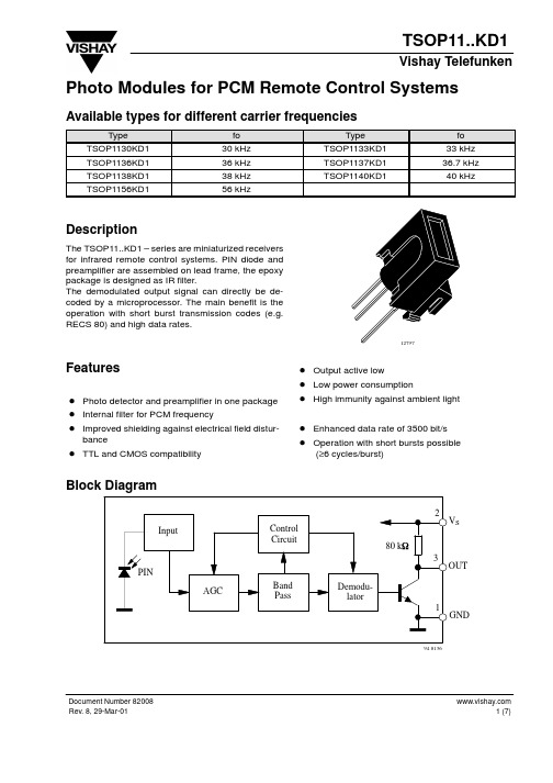
Photo Modules for PCM Remote Control Systems Available types for different carrier frequenciesTypeTSOP1130KD1TSOP1136KD1TSOP1138KD1TSOP1156KD1DescriptionThe TSOP11..KD1 – series are miniaturized receiversfor infrared remote control systems. PIN diode andpreamplifier are assembled on lead frame, the epoxypackage is designed as IR filter.The demodulated output signal can directly be de-coded by a microprocessor. The main benefit is theoperation with short burst transmission codes (e.g.RECS 80) and high data rates.UnitVmAVmA°C°C°CmW°CMax Unit 1.5mAmA 5.5VDocument Number 82008Suitable Data FormatThe circuit of the TSOP11..KD1 is designed in that way that unexpected output pulses due to noise or disturbance signals are avoided. A bandpassfilter, an integrator stage and an automatic gain control are used to suppress such disturbances.The distinguishing mark between data signal and disturbance signal are carrier frequency, burst length and duty cycle.The data signal should fullfill the following condition:•Carrier frequency should be close to center frequency of the bandpass (e.g. 38kHz).•Burst length should be 6 cycles/burst or longer.•After each burst which is between 6 cycles and 70cycles a gap time of at least 10 cycles is neccessary.•For each burst which is longer than 1.8ms a corresponding gap time is necessary at some time in the data stream. This gap time should have at least same length as the burst.•Up to 2200 short bursts per second can be received continuously.Some examples for suitable data format are:NEC Code, Toshiba Micom Format, Sharp Code, RC5Code, RC6 Code, RCMM Code, R–2000 Code,RECS–80 Code.When a disturbance signal is applied to the TSOP11..KD1 it can still receive the data signal.However the sensitivity is reduced to that level that no unexpected pulses will occure.Some examples for such disturbance signals which are suppressed by the TSOP11..KD1 are:•DC light (e.g. from tungsten bulb or sunlight)•Continuous signal at 38kHz or at any other frequency•Signals from fluorescent lamps with electronic ballast (an example of the signal modulation is in the figure below).05101520time [ms]IR Signal from Fluorescent Lamp with low Modulation2.0/m ) Figure 4. Sensitivity vs. Electric Field Disturbances1 kHzE etpi *V O V OH V OLOptical Test Signal( IR diode TSAL6200, I Output Signalt d 1 )12* t E eOptical Test Signal Document Number 8200895 11339p20.40.200.20.40.60.60.90°30°10°20°40°50°60°70°80°1.00.80.7d rel – Relative Transmission Distance Figure 13. Vertical Directivity ϕy 95 11340p20.40.200.20.40.60.60.90°30°10°20°40°50°60°70°80°1.00.80.7d rel – Relative Transmission DistanceFigure 14. Horizontal Directivity ϕxDimensions in mm12823Document Number 82008Ozone Depleting Substances Policy StatementIt is the policy of Vishay Semiconductor GmbH to1.Meet all present and future national and international statutory requirements.2.Regularly and continuously improve the performance of our products, processes, distribution and operating systems with respect to their impact on the health and safety of our employees and the public, as well as their impact on the environment.It is particular concern to control or eliminate releases of those substances into the atmosphere which are known as ozone depleting substances (ODSs).The Montreal Protocol (1987) and its London Amendments (1990) intend to severely restrict the use of ODSs and forbid their use within the next ten years. Various national and international initiatives are pressing for an earlier ban on these substances.Vishay Semiconductor GmbH has been able to use its policy of continuous improvements to eliminate the use of ODSs listed in the following documents.1.Annex A, B and list of transitional substances of the Montreal Protocol and the London Amendments respectively2.Class I and II ozone depleting substances in the Clean Air Act Amendments of 1990 by the Environmental Protection Agency (EPA) in the USA3.Council Decision 88/540/EEC and 91/690/EEC Annex A, B and C (transitional substances) respectively.Vishay Semiconductor GmbH can certify that our semiconductors are not manufactured with ozone depleting substances and do not contain such substances.We reserve the right to make changes to improve technical design and may do so without further notice.Parameters can vary in different applications. All operating parameters must be validated for each customer application by the customer. Should the buyer use Vishay-Telefunken products for any unintended or unauthorized application, the buyer shall indemnify Vishay-Telefunken against all claims, costs, damages, and expenses, arising out of, directly or indirectly, any claim of personal damage, injury or death associated with such unintended or unauthorized use.Vishay Semiconductor GmbH, P .O.B. 3535, D-74025 Heilbronn, Germany Telephone: 49 (0)7131 67 2831, Fax number: 49 (0)7131 67 2423。
BTB08中文资料
VD = VDRM RL = 3.3 kΩ Tj = 125°C IT = 100 mA IG = 1.2 IGT
■
STANDARD (4 Quadrants)
Symbol Test Conditions Quadrant BTA/BTB08 C IGT (1) V D = 12 V VGT VGD IH (2) IL dV/dt (2) V D = VDRM RL = 3.3 kΩ Tj = 125°C IT = 500 mA IG = 1.2 IGT V D = 67 %VDRM gate open Tj = 125°C Tj = 125°C I - III - IV II MIN. MIN. RL = 30 Ω I - II - III IV ALL ALL MAX. MAX. MIN. MAX. MAX. 25 40 80 200 5 25 50 1.3 0.2 50 50 100 400 10 V/µs V/µs B 50 100 mA V V mA mA Unit
(dV/dt)c (2) (dI/dt)c = 3.5 A/ms
STATIC CHARACTERISTICS
Symbol VTM (2) Vto (2) Rd (2) I DRM I RRM
Note 1: minimum IGT is guaranted at 5% of IGT max. Note 2: for both polarities of A2 referenced to A1
Type Standard Snubberless Standard Snubberless Logic level Logic level Logic level Logic level Snubberless Snubberless Snubberless
k8030聚丙烯参数

k8030聚丙烯参数英文回答:Polypropylene is a versatile thermoplastic polymer that is widely used in various industries due to its excellent properties. As for the K8030 polypropylene, it possesses several key parameters that make it suitable for specific applications.Firstly, the melt flow rate (MFR) of K8030 polypropylene is an important parameter to consider. MFR refers to the rate at which the polymer flows under a specified load and temperature. It is measured in grams per 10 minutes (g/10 min). A high MFR indicates that the polymer has good flowability, which is desirable for processes such as injection molding or extrusion. On the other hand, a low MFR indicates a more viscous polymer, which may be preferred for applications requiring higher stiffness or dimensional stability.Secondly, the density of K8030 polypropylene is another significant parameter. Density is the mass per unit volume and is usually expressed in grams per cubic centimeter(g/cm³). The density of polypropylene affects its mechanical properties, such as stiffness and impact resistance. Higher density polypropylene tends to havebetter stiffness but lower impact resistance, while lower density polypropylene exhibits the opposite characteristics. Therefore, the density of K8030 polypropylene should be chosen based on the specific requirements of the application.Moreover, the tensile strength and elongation at break are crucial parameters to evaluate the mechanical performance of K8030 polypropylene. Tensile strength measures the maximum stress a material can withstand before breaking, while elongation at break indicates the abilityof the material to stretch before failure. These parameters are essential for applications that require high strength and durability, such as automotive parts or packaging materials. K8030 polypropylene offers a balance between tensile strength and elongation at break, making itsuitable for various demanding applications.Furthermore, the thermal properties of K8030 polypropylene should not be overlooked. The melting point and heat deflection temperature (HDT) are two important parameters in this regard. The melting point is the temperature at which the polymer transitions from a solid to a liquid state, while the HDT is the temperature at which the polymer deforms under a specified load. These properties determine the heat resistance and processing temperature range of K8030 polypropylene. For example, if a product needs to withstand high temperatures, a polypropylene with a higher melting point and HDT should be selected.In summary, the key parameters of K8030 polypropylene include melt flow rate, density, tensile strength, elongation at break, melting point, and heat deflection temperature. These parameters play a crucial role in determining the suitability of K8030 polypropylene for specific applications. By considering these parameters, manufacturers can make informed decisions and select themost appropriate material for their desired applications.中文回答:聚丙烯是一种多功能的热塑性聚合物,在各个行业广泛应用,其优异的性能使其成为理想的材料。
KB827-B中文资料

GENERAL PURPOSEHIGH ISOLATION VOLTAGESINGLE TRANSISTOR TYPEPHOTOCOUPLER SERIESFEATURES1.High isolation voltage between input and output (Viso=5000 Vrms).pact dual-in-line packageKB827:2-channel type3.Recognized by UL and CUL, file NO.E225308.4.Approved by VDE 0884 Teil2(NO:40006364)(Creepage distance between input and output:7mm or more).5.Rohs compliant.DESCRIPTION1.The KB827 (2-channel) is optically coupled isolators containing a GaAS light emitting diode and an NPN silicon phototransistor.2.The lead pitch is 2.54mm.3.Solid insulation thickness between emitting diode and output phototransistor:>=0.6mm.APPLICATIONSputer terminals.2.Registers,copiers,automatic vending machines.3.System appliances, measuring instruments.4.Programmable logic controller.5.Signal transmission between circuits of different potentials and impedances.Parameter Symbol Rating UnitInput Forward current IF50mAReverse voltage VR6V Power dissipation P70mWOutput Collector-emitter voltage VC E O35VEmitter-collector voltage VE C O6VCollector current IC50mACollector power dissipation PC150mWT otal power dissipation Ptot200mW *1Isolation voltage Viso5000Vrms Operating temperature T opr-30~+100°C Storage temperature T stg-55~+125°C *2Soldering temperature T sol260°C *140 to 60% RH,AC for 1 minute.*2For 10 seconds.Flux Rosin flux containing small amount of chorine(The flux with a maximum chlorine content of 0.2 Wt % is recommended.)(2) CautionsFluxesAvoid removing the residual flux with freon-based and chlorine-based cleaning solvent.2.Cautions regarding noiseBe aware that power is suddenly into the componment any surge current may cause damage happen, even if the voltage is within the absolute maximum ratings.CAUTIONWithin this device there exists GaAs (Gallium Arsenide) material which is a harmful substance if。
K9K8G08U0B-PCBO
K9K8G08U0BK9WAG08U1BINFORMATION IN THIS DOCUMENT IS PROVIDED IN RELATION TO SAMSUNG PRODUCTS, AND IS SUBJECT TO CHANGE WITHOUT NOTICE.NOTHING IN THIS DOCUMENT SHALL BE CONSTRUED AS GRANTING ANY LICENSE, EXPRESS OR IMPLIED, BY ESTOPPEL OR OTHERWISE,TO ANY INTELLECTUAL PROPERTY RIGHTS IN SAMSUNG PRODUCTS OR TECHNOLOGY. ALL INFORMATION IN THIS DOCUMENT IS PROVIDEDON AS "AS IS" BASIS WITHOUT GUARANTEE OR WARRANTY OF ANY KIND.1. For updates or additional information about Samsung products, contact your nearest Samsung office.2. Samsung products are not intended for use in life support, critical care, medical, safety equipment, or similar applications where Product failure could result in loss of life or personal or physical harm, or any military or defense application, or any governmental procurement to which special terms or provisions may apply.* Samsung Electronics reserves the right to change products or specification without notice.Document Title1G x 8 / 2G x 8 Bit NAND Flash Memory Revision HistoryThe attached data sheets are prepared and approved by SAMSUNG Electronics. SAMSUNG Electronics CO., LTD. reserve the rightto change the specifications. SAMSUNG Electronics will evaluate and reply to your requests and questions about device. If you have any questions, please contact the SAMSUNG branch office near your office.Revision No0.00.1RemarkAdvance AdvanceHistory 1. Initial issue1. K9K8G08U0B-P is added.Draft DateJun. 11, 2008Jul. 10, 2008GENERAL DESCRIPTIONFEATURES• Voltage Supply- 3.3V (2.70V ~ 3.60V)• Organization- Memory Cell Array :- K9K8G08U0B : (1G + 32M) x 8bit - K9WAG08U1B : (2G + 64M) x 8bit - Data Register : (2K + 64) x 8bit • Automatic Program and Erase - Page Program : (2K + 64)Byte - Block Erase : (128K + 4K)Byte • Page Read Operation- Page Size : (2K + 64)Byte - Random Read : 25µs(Max.) - Serial Access : 25ns(Min.)1G x 8 / 2G x 8 Bit NAND Flash Memory• Fast Write Cycle Time- Page Program time : 200µs(Typ.) - Block Erase Time : 1.5ms(Typ.)• Command/Address/Data Multiplexed I/O Port • Hardware Data Protection- Program/Erase Lockout During Power Transitions • Reliable CMOS Floating-Gate Technology- Endurance : 100K Program/Erase Cycles (with 1bit/528Byte ECC)- Data Retention : 10 Years • Command Driven Operation• Unique ID for Copyright Protection • Package :- K9K8G08U0B-PCB0/PIB048 - Pin TSOP I (12 x 20 / 0.5 mm pitch) - K9WAG08U1B-PCB0/PIB048 - Pin TSOP I (12 x 20 / 0.5 mm pitch) - K9WAG08U1B-ICB0/IIB052 - Pin ULGA (12 x 17 / 1.0 mm pitch)Offered in 1G x 8bit, the K9K8G08U0B is a 8G-bit NAND Flash Memory with spare 256M-bit. And the K9WAG08U1B is a 16G-bit NAND Flash Memory with spare 512M-bit. Its NAND cell provides the most cost-effective solution for the solid state application mar-ket. A program operation can be performed in typical 200µs on the (2K+64)Byte page and an erase operation can be performed in typical 1.5ms on a (128K+4K)Byte block. Data in the data register can be read out at 25ns cycle time per Byte. The I/O pins serve as the ports for address and data input/output as well as command input. The on-chip write controller automates all program and erase functions including pulse repetition, where required, and internal verification and margining of data. Even the write-intensive systems can take advantage of the K9K8G08U0B/K9WAG08U1B ′s extended reliability of 100K program/erase cycles by providing ECC(Error Correcting Code) with real time mapping-out algorithm. The K9K8G08U0B/K9WAG08U1B is an optimum solution for large nonvola-tile storage applications such as solid state file storage and other portable applications requiring non-volatility.PRODUCT LISTPart Number Vcc RangeOrganizationPKG Type K9K8G08U0B-P 2.70 ~ 3.60VX8TSOP1K9WA G08U1B-P K9WA G08U1B-I52ULGA1.001.001.001.002.007 6 5 4 3 2 11.001.001.0012.00±0.10#A117.00±0.1017.00±0.10BA12.00±0.10(Datum B)(Datum A)12.0010.002.502.502.000.501.30A B C DEF GHJ K L M N12-∅1.00±0.0541-∅0.70±0.05Side View1.0(M a x .)0.10 C17.00±0.10Top ViewBottom ViewABC D EF G H J KL M N7654321K9WAG08U1B-ICB0/IIB052ULGA (measured in millimeters)NCNCNCNCNCNCNCNCNC NCNCNCNCNCNC NCVccVcc VssVssVss /RE1/RE2/CE1/CE2CLE1CLE2ALE1ALE2/WE1/WE2/WP1/WP2R/B1R/B2VssIO0-1IO0-2IO1-1IO1-2IO2-1IO3-1IO2-2IO3-2IO4-1IO4-2IO5-1IO5-2IO6-1IO6-2IO7-1IO7-2∅ABC M 0.1∅ABC M 0.1PACKAGE DIMENSIONSPIN DESCRIPTIONNOTE : Connect all V CC and V SS pins of each device to common power supply outputs. Do not leave V CC or V SS disconnected.Pin Name Pin FunctionI/O 0 ~ I/O 7DATA INPUTS/OUTPUTSThe I/O pins are used to input command, address and data, and to output data during read operations. The I/O pins float to high-z when the chip is deselected or when the outputs are disabled.CLECOMMAND LATCH ENABLEThe CLE input controls the activating path for commands sent to the command register. When active high, commands are latched into the command register through the I/O ports on the rising edge of the WE signal.ALEADDRESS LATCH ENABLEThe ALE input controls the activating path for address to the internal address registers. Addresses are latched on the rising edge of WE with ALE high.CE / CE1CHIP ENABLEThe CE / CE1 input is the device selection control. When the device is in the Busy state, CE / CE1 high is ignored, and the device does not return to standby mode in program or erase operation.Regarding CE / CE1 control during read operation , refer to ’Page Read’ section of Device operation. CE2CHIP ENABLEThe CE2 input enables the second of K9WAG08U1B.REREAD ENABLEThe RE input is the serial data-out control, and when active drives the data onto the I/O bus. Data is valid tREA after the falling edge of RE which also increments the internal column address counter by one.WEWRITE ENABLEThe WE input controls writes to the I/O port. Commands, address and data are latched on the rising edge of the WE pulse.WPWRITE PROTECTThe WP pin provides inadvertent program/erase protection during power transitions. The internal high volt-age generator is reset when the WP pin is active low.R/B / R/B1READY/BUSY OUTPUTThe R/B / R/B1 output indicates the status of the device operation. When low, it indicates that a program, erase or random read operation is in process and returns to high state upon completion. It is an open drain output and does not float to high-z condition when the chip is deselected or when outputs are disabled.Vcc POWERV CC is the power supply for device. Vss GROUNDN.CNO CONNECTIONLead is not internally connected.Product IntroductionThe K9K8G08U0B has a 8,448Mbit(8,858,370,048 bit) memory organized as 524,288 rows(pages) by 2,112x8 columns. Spare 64x8 columns are located from column address of 2,048~2,111. A 2,112-byte data register is connected to memory cell arrays accommo-dating data transfer between the I/O buffers and memory during page read and page program operations. The memory array is made up of 32 cells that are serially connected to form a NAND structure. Each of the 32 cells resides in a different page. A block consists of two NAND structured strings. A NAND structure consists of 32 cells. Total 1,081,344 NAND cells reside in a block. The program and read operations are executed on a page basis, while the erase operation is executed on a block basis. The memory array con-sists of 8,192 separately erasable 128K-byte blocks. It indicates that the bit by bit erase operation is prohibited on the K9K8G08U0B. The K9K8G08U0B has addresses multiplexed into 8 I/Os. This scheme dramatically reduces pin counts and allows system upgrades to future densities by maintaining consistency in system board design. Command, address and data are all written through I/O's by bringing WE to low while CE is low. Those are latched on the rising edge of WE. Command Latch Enable(CLE) and Address Latch Enable(ALE) are used to multiplex command and address respectively, via the I/O pins. Some commands require one bus cycle. For example, Reset Command, Status Read Command, etc require just one cycle bus. Some other commands, like page read and block erase and page program, require two cycles: one cycle for setup and the other cycle for execution. The 1,056M byte physical space requires 31 addresses, thereby requiring five cycles for addressing : 2 cycles of column address, 3 cycles of row address, in that order. Page Read and Page Program need the same five address cycles following the required command input. In Block Erase oper-ation, however, only the three row address cycles are used. Device operations are selected by writing specific commands into the command register. Table 1 defines the specific commands of the K9K8G08U0B.In addition to the enhanced architecture and interface, the device incorporates copy-back program feature from one page to another page without need for transporting the data to and from the external buffer memory. Since the time-consuming serial access and data-input cycles are removed, system performance for solid-state disk application is significantly increased.The K9WAG08U1B is composed of two K9K8G08U0B chips which are selected separately by each CE1 and CE2.Table 1. Command SetsFunction1st Cycle2nd Cycle Acceptable Command during Busy Read 00h30hRead for Copy Back00h35hRead ID90h-Reset FFh-OPage Program80h10hTwo-Plane Page Program(3)80h---11h81h---10hCopy-Back Program85h10hTwo-Plane Copy-Back Program(3)85h---11h81h---10hBlock Erase60h D0hTwo-Plane Block Erase60h---60h D0hRandom Data Input(1)85h-Random Data Output(1)05h E0hRead Status70h OChip1 Status(2)F1h OChip2 Status(2)F2h ONOTE : 1. Random Data Input/Output can be executed in a page.2. Interleave-operation between two chips is allowed.It’s prohibited to use F1h and F2h commands for other operations except interleave-operation.3.Any command between 11h and 81h is prohibited except 70h, F1h, F2h and FFh .Caution : Any undefined command inputs are prohibited except for above command set of Table 1.DC AND OPERATING CHARACTERISTICS (Recommended operating conditions otherwise noted.)NOTE : 1. V IL can undershoot to -0.4V and V IH can overshoot to V CC +0.4V for durations of 20 ns or less. 2. Typical value is measured at Vcc=3.3V, T A =25°C. Not 100% tested.3. The maximum value of K9K8G08U0B -P’s I LI and I LO is ±40µA , the maximum value of K9K8G08U0B -I’s I LI and I LO is ±20µA .ParameterSymbol Test ConditionsMinTypMaxUnitOperating CurrentPage Read withSerial Access I CC 1tRC=25nsCE=V IL, I OUT =0mA-2535mAProgramI CC 2-EraseI CC 3-Stand-by Current(TTL)I SB 1CE=V IH , WP=0V/V CC --1Stand-by Current(CMOS)I SB 2CE=V CC -0.2, WP=0V/V CC -40200µAInput Leakage Current I LI V IN =0 to Vcc(max)--±40Output Leakage Current I LO V OUT =0 to Vcc(max)--±40Input High VoltageV IH (1)-0.8xVcc -Vcc+0.3V Input Low Voltage, All inputs V IL (1)--0.3-0.2xVccOutput High Voltage Level V OH I OH =-400µA 2.4--Output Low Voltage Level V OL I OL =2.1mA --0.4Output Low Current(R/B)I OL (R/B)V OL =0.4V810-mA RECOMMENDED OPERATING CONDITIONS(Voltage reference to GND, K9XXG08UXB-XCB0 :T A =0 to 70°C, K9XXG08UXB-XIB0:T A =-40 to 85°C)ParameterSymbol Min Typ.Max Unit Supply Voltage V CC 2.7 3.3 3.6V Supply VoltageV SSVABSOLUTE MAXIMUM RATINGSNOTE :1. Minimum DC voltage is -0.6V on input/output pins. During transitions, this level may undershoot to -2.0V for periods <30ns. Maximum DC voltage on input/output pins is V CC +0.3V which, during transitions, may overshoot to V CC +2.0V for periods <20ns.2. Permanent device damage may occur if ABSOLUTE MAXIMUM RATINGS are exceeded. Functional operation should be restricted to the conditions as detailed in the operational sections of this data sheet. Exposure to absolute maximum rating conditions for extended periods may affect reliability.ParameterSymbol Rating Unit Voltage on any pin relative to VSSV CC -0.6 to +4.6VV IN -0.6 to +4.6V I/O-0.6 to Vcc+0.3 (<4.6V)Temperature Under Bias K9XXG08UXB-XCB0T BIAS -10 to +125°C K9XXG08UXB-XIB0-40 to +125Storage Temperature K9XXG08UXB-XCB0T STG-65 to +150°CK9XXG08UXB-XIB0Short Circuit CurrentI OS5mACAPACITANCE (T A =25°C, V CC =3.3V, f=1.0MHz)NOTE : Capacitance is periodically sampled and not 100% tested. K9WAG08U1B-IXB0’s capacitance(I/O, Input) is 20pF.ItemSymbol Test ConditionMin MaxUnitK9K8G08U0BK9WAG08U1B*Input/Output Capacitance C I/O V IL =0V -2040pF Input CapacitanceC INV IN =0V-2040pF VALID BLOCKNOTE :1. The device may include initial invalid blocks when first shipped. Additional invalid blocks may develop while being used. The number of valid blocks is presented with both cases of invalid blocks considered. Invalid blocks are defined as blocks that contain one or more bad bits. Do not erase or pro-gram factory-marked bad blocks. Refer to the attached technical notes for appropriate management of invalid blocks.2. The 1st block, which is placed on 00h block address, is guaranteed to be a valid block up to 1K program/erase cycles with 1bit/528Byte ECC.3. The number of valid block is on the basis of single plane operations, and this may be decreased with two plane operations.* : Each K9K8G08U0B chip in the K9WAG08U1B has Maximun 160 invalid blocks.Parameter Symbol Min Typ.Max Unit K9K8G08U0B N VB8,028-8,192BlocksK9WAG08U1B16,064*-16,384*AC TEST CONDITION(K9XXG08UXB-XCB0: T A =0 to 70°C, K9XXG08UXB-XIB0:T A =-40 to 85°C ,K9XXG08UXB: Vcc=2.7V~3.6V unless otherwise noted)ParameterK9WAG08U1B Input Pulse Levels 0V to Vcc Input Rise and Fall Times 5ns Input and Output Timing Levels Vcc/2Output Load1 TTL GATE and CL=50pF (K9K8G08U0B-P/K9WAG08U1B-I)1 TTL GATE and CL=30pF (K9WAG08U1B-P)MODE SELECTIONNOTE : 1. X can be V IL or V IH.2. WP should be biased to CMOS high or CMOS low for standby.CLE ALE CE WERE WP ModeH L L H X Read Mode Command Input L H L H X Address Input(5clock)H L L H H Write Mode Command Input L H L H H Address Input(5clock)L L L HH Data Input L L L H X Data Output X X X X H X During Read(Busy)X X X X X H During Program(Busy)X X X X X H During Erase(Busy)X X (1)X X X L Write Protect XXHXX0V/V CC (2)Stand-byProgram / Erase CharacteristicsParameter Symbol Min Typ Max Unit Program Time t PROG-200700µs Dummy Busy Time for Two-Plane Page Program t DBSY-0.51µs Number of Partial Program Cycles Nop--4cycles Block Erase Time t BERS- 1.52msNOTE : 1. Typical value is measured at Vcc=3.3V, T A=25°C. Not 100% tested.2. Typical program time is defined as the time within which more than 50% of the whole pages are programmed at3.3V Vcc and 25°C tempera-ture.AC Timing Characteristics for Command / Address / Data InputParameter Symbol Min Max UnitCLE Setup Time t CLS(1)12-nsCLE Hold Time t CLH5-nsCE Setup Time t CS(1)20-nsCE Hold Time t CH5-nsWE Pulse Width t WP12-nsALE Setup Time t ALS(1)12-nsALE Hold Time t ALH5-nsData Setup Time t DS(1)12-nsData Hold Time t DH5-nsWrite Cycle Time t WC25-nsWE High Hold Time t WH10-nsAddress to Data Loading Time t ADL(2)70-nsNOTES : 1. The transition of the corresponding control pins must occur only once while WE is held low.2. tADL is the time from the WE rising edge of final address cycle to the WE rising edge of first data cycle.AC Characteristics for OperationParameter Symbol Min Max Unit Data Transfer from Cell to Register t R-25µs ALE to RE Delay t AR10-ns CLE to RE Delay t CLR10-ns Ready to RE Low t RR20-ns RE Pulse Width t RP12-ns WE High to Busy t WB-100ns Read Cycle Time t RC25-ns RE Access Time t REA-20ns CE Access Time t CEA-25ns RE High to Output Hi-Z t RHZ-100ns CE High to Output Hi-Z t CHZ-30ns RE High to Output hold t RHOH15-ns RE Low to Output hold t RLOH5-ns CE High to Output hold t COH15-ns RE High Hold Time t REH10-ns Output Hi-Z to RE Low t IR0-ns RE High to WE Low t RHW100-ns WE High to RE Low t WHR60-ns Device Resetting Time(Read/Program/Erase)t RST-5/10/500(1)µs NOTE: 1. If reset command(FFh) is written at Ready state, the device goes into Busy for maximum 5µs.NAND Flash Technical NotesIdentifying Initial Invalid Block(s)Initial Invalid Block(s)Initial invalid blocks are defined as blocks that contain one or more initial invalid bits whose reliability is not guaranteed by Samsung.The information regarding the initial invalid block(s) is called the initial invalid block information. Devices with initial invalid block(s)have the same quality level as devices with all valid blocks and have the same AC and DC characteristics. An initial invalid block(s)does not affect the performance of valid block(s) because it is isolated from the bit line and the common source line by a select tran-sistor. The system design must be able to mask out the initial invalid block(s) via address mapping. The 1st block, which is placed on 00h block address, is guaranteed to be a valid block up to 1K program/erase cycles with 1bit /528Byte ECC.All device locations are erased(FFh) except locations where the initial invalid block(s) information is written prior to shipping. The ini-tial invalid block(s) status is defined by the 1st byte in the spare area. Samsung makes sure that either the 1st or 2nd page of every initial invalid block has non-FFh data at the column address of 2,048. Since the initial invalid block information is also erasable in most cases, it is impossible to recover the information once it has been erased. Therefore, the system must be able to recognize the initial invalid block(s) based on the original initial invalid block information and create the initial invalid block table via the following suggested flow chart(Figure 3). Any intentional erasure of the original initial invalid block information is prohibited.*Check "FFh" at the column address 2,048 Figure 3. Flow chart to create initial invalid block table.StartSet Block Address = 0Check "FFh"Increment Block AddressLast Block ?EndNoYesYesCreate (or update)NoInitialof the 1st and 2nd page in the blockInvalid Block(s) TableNAND Flash Technical Notes (Continued)Program Flow ChartStartI/O 6 = 1 ?I/O 0 = 0 ?No*Write 80hWrite AddressWrite DataWrite 10hRead Status RegisterProgram Completedor R/B = 1 ?Program ErrorYesNoYes: If program operation results in an error, map out the block including the page in error and copy thetarget data to another block.*Error in write or read operationWithin its life time, additional invalid blocks may develop with NAND Flash memory. Refer to the qualification report for the actual data.The following possible failure modes should be considered to implement a highly reliable system. In the case of status read fail-ure after erase or program, block replacement should be done. Because program status fail during a page program does not affect the data of the other pages in the same block, block replacement can be executed with a page-sized buffer by finding an erased empty block and reprogramming the current target data and copying the rest of the replaced block. In case of Read, ECC must be employed. To improve the efficiency of memory space, it is recommended that the read or verification failure due to single bit error be reclaimed by ECC without any block replacement. The said additional block failure rate does not include those reclaimed blocks.Failure ModeDetection and Countermeasure sequenceWrite Erase Failure Status Read after Erase --> Block Replacement Program Failure Status Read after Program --> Block Replacement ReadSingle Bit FailureVerify ECC -> ECC CorrectionECC: Error Correcting Code --> Hamming Code etc. Example) 1bit correction & 2bit detectionInterleave Page ProgramK9WAG08U1B is composed of two K9K8G08U0Bs. And K9K8G08U0B also is composed of two K9F4G08U0Bs. K9K8G08U0B pro-vides interleaving operation between two K9F4G08U0Bs.This interleaving page program improves the system throughput almost twice compared to non-interleaving page program.At first, the host issues page program command to one of the K9F4G08U0B chips, say K9F4G08U0B(chip #1). Due to this K9K8G08U0B goes into busy state. During this time, K9F4G08U0B(chip #2) is in ready state. So it can execute the page program command issued by the host.After the execution of page program by K9F4G08U0B(chip #1), it can execute another page program regardless of the K9F4G08U0B(chip #2). Before that the host needs to check the status of K9F4G08U0B(chip #1) by issuing F1h command. Only when the status of K9F4G08U0B(chip #1) becomes ready status, host can issue another page program command. If the K9F4G08U0B(chip #1) is in busy state, the host has to wait for the K9F4G08U0B(chip #1) to get into ready state.Similarly, K9F4G08U0B chip(chip #2) can execute another page program after the completion of the previous program. The host can monitor the status of K9F4G08U0B(chip #2) by issuing F2h command. When the K9F4G08U0B(chip #2) shows ready state, host can issue another page program command to K9F4G08U0B(chip #2).This interleaving algorithm improves the system throughput almost twice. The host can issue page program command to each chip individually. This reduces the time lag for the completion of operation.NOTES : During interleave operations, 70h command is prohibited.R / B (#1)b u s y o f C h i p #1I /O X80h10h C o m m a n d A 30 : L o w A d d & D a t a80h 10h A 30 : H i g h A d d & D a t ab u s y o f C h i p #2i n t e r n a l o n l yR /B (#2)i n t e r n a l o n l yR /BI n t e r l e a v e P a g e P r o g r a m≈≈≈F 1h o r F 2h A B CDa n o t h e r p a g e p r o g r a m o n C h i p #1S t a t e A : C h i p #1 i s e x e c u t i n g a p a g e p r o g r a m o p e r a t i o n a n d c h i p #2 i s i n r e a d y s t a t e . S o t h e h o s t c a n i s s u e a p a g e p r o g r a m c o m m a n d t o c h i p #2.S t a t e B : B o t h c h i p #1 a n d c h i p #2 a r e e x e c u t i n g p a g e p r o g r a m o p e r a t i o n .S t a t e C : P a g e p r o g r a m o n c h i p #1 i s t e r m i n a t e d , b u t p a g e p r o g r a m o n c h i p #2 i s s t i l l o p e r a t i n g . A n d t h e s y s t e m s h o u l d i s s u e F 1h c o m m a n d t o d e t e c t t h e s t a t u s o f c h i p #1. I f c h i p #1 i s r e a d y , s t a t u s I /O 6 i s "1" a n d t h e s y s t e m c a n i s s u e a n o t h e r p a g e p r o g r a m c o m m a n d t o c h i p #1.S t a t e D : C h i p #1 a n d C h i p #2 a r e r e a d y .A c c o r d i n g t o t h e a b o v e p r o c e s s , t h e s y s t e m c a n o p e r a t e p a g e p r o g r a m o n c h i p #1 a n d c h i p #2 a l t e r n a t e l y .S t a t u sO p e r a t i o nS t a t u s C o m m a n d / D a t aF 1hF 2hAC h i p 1 : B u s y , C h i p 2 : R e a d y8x hC x hBC h i p 1 : B u s y , C h i p 2 : B u s y8x h8x hCC h i p 1 : R e a d y , C h i p 2 : B u s yC x h8x hDC h i p 1 : R e a d y , C h i p 2 : R e a d yC x hC x hR / B (#1)b u s y o f C h i p #1I /O X60hD 0h C o m m a n d A 30 : L o w A d d60h D 0h A 30 : H i g h A d db u s y o f C h i p #2i n t e r n a l o n l yR /B (#2)i n t e r n a l o n l yR /BI n t e r l e a v e B l o c k E r a s e≈≈≈F 1h o r F 2h A B CDa n o t h e r B l o c k E r a s e o n C h i p #1S t a t e A : C h i p #1 i s e x e c u t i n g a b l o c k e r a s e o p e r a t i o n , a n d c h i p #2 i s i n r e a d y s t a t e . S o t h e h o s t c a n i s s u e a b l o c k e r a s e c o m m a n d t o c h i p #2.S t a t e B : B o t h c h i p #1 a n d c h i p #2 a r e e x e c u t i n g b l o c k e r a s e o p e r a t i o n .S t a t e C : B l o c k e r a s e o n c h i p #1 i s t e r m i n a t e d , b u t b l o c k e r a s e o n c h i p #2 i s s t i l l o p e r a t i n g . A n d t h e s y s t e m s h o u l d i s s u e F 1h c o m m a n d t o d e t e c t t h e s t a t u s o f c h i p #1. I f c h i p #1 i s r e a d y , s t a t u s I /O 6 i s "1" a n d t h e s y s t e m c a n i s s u e a n o t h e r b l o c k e r a s e c o m m a n d t o c h i p #1.S t a t e D : C h i p #1 a n d C h i p #2 a r e r e a d y .A c c o r d i n g t o t h e a b o v e p r o c e s s , t h e s y s t e m c a n o p e r a t e b l o c k e r a s e o n c h i p #1 a n d c h i p #2 a l t e r n a t e l y .S t a t u sO p e r a t i o nS t a t u s C o m m a n d / D a t aF 1hF 2hAC h i p 1 : B u s y , C h i p 2 : R e a d y8x hC x hBC h i p 1 : B u s y , C h i p 2 : B u s y8x h8x hCC h i p 1 : R e a d y , C h i p 2 : B u s yC x h8x hDC h i p 1 : R e a d y , C h i p 2 : R e a d yC x hC x hR /B (#1)I /O XC o m m a n dt B E R S o f c h i p #1i n t e r n a l o n l yR /B (#2)i n t e r n a l o n l yR /B60h D 0h A 30 :L o w A d d 60hA 30 : L o wA d d F 1h o r F 2h *60h D 0hA 30 :H i g h A d d60h A 30 : H i g h A d d t B E R S o f c h i p #2t B E R S o f c h i p #211I n t e r l e a v e T w o -P l a n e B l o c k E r a s eR /B (#1)I /O Xi n t e r n a l o n l yR /B (#2)i n t e r n a l o n l yR /B≈≈≈ABCS t a t e A : C h i p #1 i s e x e c u t i n g a b l o c k e r a s e o p e r a t i o n , a n d c h i p #2 i s i n r e a d y s t a t e . S o t h e h o s t c a n i s s u e a b l o c k e r a s e c o m m a n d t o c h i p #2.S t a t e B : B o t h c h i p #1 a n d c h i p #2 a r e e x e c u t i n g b l o c k e r a s e o p e r a t i o n .S t a t e C : B l o c k e r a s e o n c h i p #1 i s c o m p l e t e d a n d c h i p #1 i s r e a d y f o r t h e n e x t o p e r a t i o n . C h i p #2 i s s t i l l e x e c u t i n g b l o c k e r a s e o p e r a t i o n .S t a t e D : B o t h c h i p #1 a n d c h i p #2 a r e r e a d y .N o t e : *F 1h c o m m a n d i s r e q u i r e d t o c h e c k t h e s t a t u s o f c h i p #1 t o i s s u e t h e n e x t b l o c k e r a s e c o m m a n d t o c h i p #1. F 2h c o m m a n d i s r e q u i r e d t o c h e c k t h e s t a t u s o f c h i p #2 t o i s s u e t h e n e x t b l o c k e r a s e c o m m a n d t o c h i p #2.A s t h e a b o v e p r o c e s s , t h e s y s t e m c a n o p e r a t e t w o -p l a n e b l o c k e r a s e o n c h i p #1 a n d c h i p #2 a l t e r n a t i v e l y .DRead ID OperationCECLEWEALERE90hRead ID CommandMaker Code Device Code00h ECht REAAddress 1cycleI/Oxt ARDevice Device Code(2nd Cycle)3rd Cycle 4th Cycle 5th Cycle K9K8G08U0B DCh51h95h58hK9WAG08U1BSame as K9K8G08U0BDevice 4th cyc.Code3rd cyc.5th cyc.。