ZXTAM322TA;中文规格书,Datasheet资料
MAX3222CAP+T中文资料

________________General DescriptionThe MAX3222/MAX3232/MAX3237/MAX3241 trans-ceivers have a proprietary low-dropout transmitter out-put stage enabling true RS-232 performance from a 3.0V to 5.5V supply with a dual charge pump. The devices require only four small 0.1µF external charge-pump capacitors. The MAX3222, MAX3232, and MAX3241 are guaranteed to run at data rates of 120kbps while maintaining RS-232 output levels. The MAX3237 is guaranteed to run at data rates of 250kbps in the normal operating mode and 1Mbps in the MegaBaud™ operating mode, while maintaining RS-232output levels.The MAX3222/MAX3232 have 2 receivers and 2 drivers. The MAX3222 features a 1µA shutdown mode that reduces power consumption and extends battery life in portable systems. Its receivers remain active in shutdown mode, allowing external devices such as modems to be monitored using only 1µA supply cur-rent. The MAX3222 and MAX3232 are pin, package,and functionally compatible with the industry-standard MAX242 and MAX232, respectively.The MAX3241 is a complete serial port (3 drivers/5 receivers) designed for notebook and subnotebook computers. The MAX3237 (5 drivers/3 receivers) is ideal for fast modem applications. Both these devices feature a shutdown mode in which all receivers can remain active while using only 1µA supply current. Receivers R1(MAX3237/MAX3241) and R2 (MAX3241) have extra out-puts in addition to their standard outputs. These extra outputs are always active, allowing external devices such as a modem to be monitored without forward bias-ing the protection diodes in circuitry that may have V CC completely removed.The MAX3222, MAX3237, and MAX3241 are available in space-saving TSSOP and SSOP packages.________________________ApplicationsNotebook, Subnotebook, and Palmtop Computers High-Speed Modems Battery-Powered Equipment Hand-Held Equipment Peripherals Printers__Next Generation Device Features♦For Smaller Packaging:MAX3228E/MAX3229E: +2.5V to +5.5V RS-232Transceivers in UCSP™♦For Integrated ESD Protection:MAX3222E/MAX3232E/MAX3237E/MAX3241E*/MAX3246E: ±15kV ESD-Protected, Down to 10nA,3.0V to 5.5V, Up to 1Mbps, True RS-232Transceivers♦For Low-Voltage or Data Cable Applications:MAX3380E/MAX3381E: +2.35V to +5.5V, 1µA, 2 Tx/2 Rx RS-232 Transceivers with ±15kV ESD-Protected I/O and Logic PinsMAX3222/MAX3232/MAX3237/MAX3241*3.0V to 5.5V , Low-Power , up to 1Mbps, T rue RS-232Transceivers Using Four 0.1µF External Capacitors________________________________________________________________Maxim Integrated Products119-0273; Rev 7; 1/07*Covered by U.S. Patent numbers 4,636,930; 4,679,134; 4,777,577; 4,797,899; 4,809,152; 4,897,774; 4,999,761; and other patents pending.Typical Operating Circuits appear at end of data sheet.Ordering Information continued at end of data sheet.For pricing, delivery, and ordering information,please contact Maxim/Dallas Direct!at 1-888-629-4642, or visit Maxim’s website at .+Denotes lead-free package.M A X 3222/M A X 3232/M A X 3237/M A X 3241Transceivers Using Four 0.1µF External Capacitors2_______________________________________________________________________________________ABSOLUTE MAXIMUM RATINGSELECTRICAL CHARACTERISTICS(V CC = +3.0V to +5.5V, C1–C4 = 0.1µF (Note 2), T A = T MIN to T MAX , unless otherwise noted. Typical values are at T A = +25°C.)Stresses beyond those listed under “Absolute Maximum Ratings” may cause permanent damage to the device. These are stress ratings only, and functional operation of the device at these or any other conditions beyond those indicated in the operational sections of the specifications is not implied. Exposure to absolute maximum rating conditions for extended periods may affect device reliability.Note 1:V+ and V- can have a maximum magnitude of 7V, but their absolute difference cannot exceed 13V.V CC ...........................................................................-0.3V to +6V V+ (Note 1)...............................................................-0.3V to +7V V- (Note 1)................................................................+0.3V to -7V V+ + V- (Note 1)...................................................................+13V Input VoltagesT_IN, SHDN , EN ...................................................-0.3V to +6V MBAUD...................................................-0.3V to (V CC + 0.3V)R_IN.................................................................................±25V Output VoltagesT_OUT...........................................................................±13.2V R_OUT....................................................-0.3V to (V CC + 0.3V)Short-Circuit DurationT_OUT....................................................................ContinuousContinuous Power Dissipation (T A = +70°C)16-Pin TSSOP (derate 6.7mW/°C above +70°C).............533mW 16-Pin Narrow SO (derate 8.70mW/°C above +70°C)....696mW 16-Pin Wide SO (derate 9.52mW/°C above +70°C)........762mW 16-Pin Plastic DIP (derate 10.53mW/°C above +70°C)...842mW 18-Pin SO (derate 9.52mW/°C above +70°C)..............762mW 18-Pin Plastic DIP (derate 11.11mW/°C above +70°C)..889mW 20-Pin SSOP (derate 7.00mW/°C above +70°C).........559mW 20-Pin TSSOP (derate 8.0mW/°C above +70°C).............640mW 28-Pin TSSOP (derate 8.7mW/°C above +70°C).............696mW 28-Pin SSOP (derate 9.52mW/°C above +70°C).........762mW 28-Pin SO (derate 12.50mW/°C above +70°C).....................1W Operating Temperature RangesMAX32_ _C_ _.....................................................0°C to +70°C MAX32_ _E_ _ .................................................-40°C to +85°C Storage Temperature Range.............................-65°C to +150°C Lead Temperature (soldering, 10s).................................+300°CMAX3222/MAX3232/MAX3237/MAX3241Transceivers Using Four 0.1µF External Capacitors_______________________________________________________________________________________3TIMING CHARACTERISTICS—MAX3222/MAX3232/MAX3241(V CC = +3.0V to +5.5V, C1–C4 = 0.1µF (Note 2), T A = T MIN to T MAX , unless otherwise noted. Typical values are at T A = +25°C.)ELECTRICAL CHARACTERISTICS (continued)(V CC = +3.0V to +5.5V, C1–C4 = 0.1µF (Note 2), T A = T MIN to T MAX , unless otherwise noted. Typical values are at T A = +25°C.)M A X 3222/M A X 3232/M A X 3237/M A X 3241Transceivers Using Four 0.1µF External Capacitors4_________________________________________________________________________________________________________________________________Typical Operating Characteristics(V CC = +3.3V, 235kbps data rate, 0.1µF capacitors, all transmitters loaded with 3k Ω, T A = +25°C, unless otherwise noted.)-6-5-4-3-2-101234560MAX3222/MAX3232TRANSMITTER OUTPUT VOLTAGEvs. LOAD CAPACITANCELOAD CAPACITANCE (pF)T R A N S M I T T E R O U T P U T V O L T A G E (V )20003000100040005000246810121416182022150MAX3222/MAX3232SLEW RATEvs. LOAD CAPACITANCELOAD CAPACITANCE (pF)S L E W R A T E (V /µs )20003000100040005000510152025303540MAX3222/MAX3232SUPPLY CURRENT vs. LOAD CAPACITANCEWHEN TRANSMITTING DATALOAD CAPACITANCE (pF)S U P P L Y C U R R E N T (m A )20003000100040005000TIMING CHARACTERISTICS—MAX3237(V CC = +3.0V to +5.5V, C1–C4 = 0.1µF (Note 2), T A = T MIN to T MAX , unless otherwise noted. Typical values are at T A = +25°C.)Note 2:MAX3222/MAX3232/MAX3241: C1–C4 = 0.1µF tested at 3.3V ±10%; C1 = 0.047µF, C2–C4 = 0.33µF tested at 5.0V ±10%.MAX3237: C1–C4 = 0.1µF tested at 3.3V ±5%; C1–C4 = 0.22µF tested at 3.3V ±10%; C1 = 0.047µF, C2–C4 = 0.33µF tested at 5.0V ±10%.Note 3:Transmitter input hysteresis is typically 250mV.MAX3222/MAX3232/MAX3237/MAX3241Transceivers Using Four 0.1µF External Capacitors_______________________________________________________________________________________5-7.5-5.0-2.502.55.07.50MAX3241TRANSMITTER OUTPUT VOLTAGEvs. LOAD CAPACITANCELOAD CAPACITANCE (pF)T R A N S M I T T E R O U T P U T V O L T A G E (V )2000300010004000500046810121416182022240MAX3241SLEW RATEvs. LOAD CAPACITANCELOAD CAPACITANCE (pF)S L E W R A T E (V /µs )20003000100040005000510152025303545400MAX3241SUPPLY CURRENT vs. LOADCAPACITANCE WHEN TRANSMITTING DATALOAD CAPACITANCE (pF)S U P P L Y C U R R E N T (m A )20003000100040005000-7.5-5.0-2.502.55.07.50MAX3237TRANSMITTER OUTPUT VOLTAGE vs. LOAD CAPACITANCE (MBAUD = GND)LOAD CAPACITANCE (pF)T R A N S M I T T E R O U T P U T V O L T A G E (V )200030001000400050000102030504060700MAX3237SLEW RATE vs. LOAD CAPACITANCE(MBAUD = V CC )LOAD CAPACITANCE (pF)S L E W R A T E (V /µs )500100015002000-7.5-5.0-2.502.55.07.50MAX3237TRANSMITTER OUTPUT VOLTAGE vs. LOAD CAPACITANCE (MBAUD = V CC )LOAD CAPACITANCE (pF)T R A N S M I T T E R O U T P U T V O L T A G E (V )5001000150020001020304050600MAX3237SUPPLY CURRENT vs.LOAD CAPACITANCE (MBAUD = GND)LOAD CAPACITANCE (pF)S U P P L Y C U R R E N T (m A )200030001000400050000246810120MAX3237SLEW RATE vs. LOAD CAPACITANCE(MBAUD = GND)LOAD CAPACITANCE (pF)S L E W R A T E (V /µs )2000300010004000500010302040506070MAX3237SKEW vs. LOAD CAPACITANCE(t PLH - t PHL )LOAD CAPACITANCE (pF)1000150050020002500_____________________________Typical Operating Characteristics (continued)(V CC = +3.3V, 235kbps data rate, 0.1µF capacitors, all transmitters loaded with 3k Ω, T A = +25°C, unless otherwise noted.)M A X 3222/M A X 3232/M A X 3237/M A X 3241Transceivers Using Four 0.1µF External Capacitors6_____________________________________________________________________________________________________________________________________________________Pin DescriptionMAX3222/MAX3232/MAX3237/MAX3241Transceivers Using Four 0.1µF External Capacitors_______________________________________________________________________________________7_______________Detailed DescriptionDual Charge-Pump Voltage ConverterThe MAX3222/MAX3232/MAX3237/MAX3241’s internal power supply consists of a regulated dual charge pump that provides output voltages of +5.5V (doubling charge pump) and -5.5V (inverting charge pump), regardless of the input voltage (V CC ) over the 3.0V to 5.5V range. The charge pumps operate in a discontinuous mode; if the output voltages are less than 5.5V, the charge pumps are enabled, and if the output voltages exceed 5.5V, the charge pumps are disabled. Each charge pump requires a flying capacitor (C1, C2) and a reservoir capacitor (C3, C4) to generate the V+ and V- supplies.RS-232 TransmittersThe transmitters are inverting level translators that con-vert CMOS-logic levels to 5.0V EIA/TIA-232 levels.The MAX3222/MAX3232/MAX3241 transmitters guaran-tee a 120kbps data rate with worst-case loads of 3k Ωin parallel with 1000pF, providing compatibility with PC-to-PC communication software (such as LapLink™).Typically, these three devices can operate at data rates of 235kbps. Transmitters can be paralleled to drive multi-ple receivers or mice.The MAX3222/MAX3237/MAX3241’s output stage is turned off (high impedance) when the device is in shut-down mode. When the power is off, the MAX3222/MAX3232/MAX3237/MAX3241 permit the outputs to be driven up to ±12V.The transmitter inputs do not have pullup resistors.Connect unused inputs to GND or V CC .MAX3237 MegaBaud OperationIn normal operating mode (MBAUD = G ND), the MAX3237 transmitters guarantee a 250kbps data rate with worst-case loads of 3k Ωin parallel with 1000pF.This provides compatibility with PC-to-PC communica-tion software, such as Laplink.For higher speed serial communications, the MAX3237features MegaBaud operation. In MegaBaud operating mode (MBAUD = V CC ), the MAX3237 transmitters guar-antee a 1Mbps data rate with worst-case loads of 3k Ωin parallel with 250pF for 3.0V < V CC < 4.5V. For 5V ±10%operation, the MAX3237 transmitters guarantee a 1Mbps data rate into worst-case loads of 3k Ωin parallel with 1000pF.Figure 1. Slew-Rate Test CircuitsLapLink is a trademark of Traveling Software, Inc.M A X 3222/M A X 3232/M A X 3237/M A X 3241Transceivers Using Four 0.1µF External Capacitors8_______________________________________________________________________________________RS-232 ReceiversThe receivers convert RS-232 signals to CMOS-logic out-put levels. The MAX3222/MAX3237/MAX3241 receivers have inverting three-state outputs. In shutdown, the receivers can be active or inactive (Table 1).The complementary outputs on the MAX3237 (R1OUTB)and the MAX3241 (R1OUTB, R2OUTB) are always active,regardless of the state of EN or SHDN . This allows for Ring Indicator applications without forward biasing other devices connected to the receiver outputs. This is ideal for systems where V CC is set to 0V in shutdown to accommodate peripherals, such as UARTs (Figure 2).MAX3222/MAX3237/MAX3241Shutdown ModeSupply current falls to less than 1µA in shutdown mode (SHDN = low). When shut down, the device’s charge pumps are turned off, V+ is pulled down to V CC , V- is pulled to ground, and the transmitter outputs are dis-abled (high impedance). The time required to exit shut-down is typically 100µs, as shown in Figure 3. Connect SHDN to V CC if the shutdown mode is not used. SHDN has no effect on R_OUT or R_OUTB.MAX3222/MAX3237/MAX3241Enable ControlThe inverting receiver outputs (R_OUT) are put into a high-impedance state when EN is high. The complemen-tary outputs R1OUTB and R2OUTB are always active,regardless of the state of EN and SHDN (Table 1). EN has no effect on T_OUT.__________Applications InformationCapacitor SelectionThe capacitor type used for C1–C4 is not critical for proper operation; polarized or nonpolarized capacitors can be used. The charge pump requires 0.1µF capaci-tors for 3.3V operation. For other supply voltages, refer to Table 2 for required capacitor values. Do not use values lower than those listed in Table 2. Increasing the capaci-tor values (e.g., by a factor of 2) reduces ripple on the transmitter outputs and slightly reduces power consump-tion. C2, C3, and C4 can be increased without changing C1’s value. However, do not increase C1 without also increasing the values of C2, C3, and C4, to maintain the proper ratios (C1 to the other capacitors).When using the minimum required capacitor values,make sure the capacitor value does not degrade exces-sively with temperature. If in doubt, use capacitors with a higher nominal value. The capacitor’s equivalent series resistance (ESR), which usually rises at low tempera-tures, influences the amount of ripple on V+ and V-.Figure 2. Detection of RS-232 Activity when the UART and Interface are Shut Down; Comparison of MAX3237/MAX3241(b) with Previous Transceivers (a).MAX3222/MAX3232/MAX3237/MAX3241Transceivers Using Four 0.1µF External Capacitors_______________________________________________________________________________________9Power-Supply DecouplingIn most circumstances, a 0.1µF bypass capacitor is adequate. In applications that are sensitive to power-supply noise, decouple V CC to ground with a capacitor of the same value as charge-pump capacitor C1. Connect bypass capacitors as close to the IC as possible.Operation Down to 2.7VTransmitter outputs will meet EIA/TIA-562 levels of ±3.7V with supply voltages as low as 2.7V.Transmitter Outputs whenExiting ShutdownFigure 3 shows two transmitter outputs when exiting shutdown mode. As they become active, the two trans-mitter outputs are shown going to opposite RS-232 lev-els (one transmitter input is high, the other is low).Each transmitter is loaded with 3k Ωin parallel with 2500pF. The transmitter outputs display no ringing or undesirable transients as they come out of shutdown.Note that the transmitters are enabled only when the magnitude of V- exceeds approximately 3V.Mouse DriveabilityThe MAX3241 has been specifically designed to power serial mice while operating from low-voltage power sup-plies. It has been tested with leading mouse brands from manufacturers such as Microsoft and Logitech. The MAX3241 successfully drove all serial mice tested and met their respective current and voltage requirements.Figure 4a shows the transmitter output voltages under increasing load current at 3.0V. Figure 4b shows a typical mouse connection using the MAX3241.CC = 3.3V C1–C4 = 0.1µF50µs/divFigure 3. Transmitter Outputs when Exiting Shutdown or Powering UpM A X 3222/M A X 3232/M A X 3237/M A X 3241Transceivers Using Four 0.1µF External Capacitors10______________________________________________________________________________________Figure 4b. Mouse Driver Test Circuit Figure 4a. MAX3241 Transmitter Output Voltage vs. Load Current per TransmitterMAX3222/MAX3232/MAX3237/MAX3241Transceivers Using Four 0.1µF External Capacitors______________________________________________________________________________________11High Data RatesThe MAX3222/MAX3232/MAX3241 maintain the RS-232±5.0V minimum transmitter output voltage even at high data rates. Figure 5 shows a transmitter loopback test circuit. Figure 6 shows a loopback test result at 120kbps, and Figure 7 shows the same test at 235kbps.For Figure 6, all transmitters were driven simultaneously at 120kbps into RS-232 loads in parallel with 1000pF.For Figure 7, a single transmitter was driven at 235kbps,and all transmitters were loaded with an RS-232 receiver in parallel with 1000pF.The MAX3237 maintains the RS-232 ±5.0V minimum transmitter output voltage at data rates up to 1Mbps.Figure 8 shows a loopback test result at 1Mbps with MBAUD = V CC . For Figure 8, all transmitters were loaded with an RS-232 receiver in parallel with 250pF.CC = 3.3V5µs/divFigure 5. Loopback Test CircuitFigure 6. MAX3241 Loopback Test Result at 120kbpsCC = 3.3V2µs/divFigure 7. MAX3241 Loopback Test Result at 235kbps0V +5V 0V -5V +5V 0VT_INT_OUT = R_IN 5k R_OUT 150pF200ns/divCC = 3.3VFigure 8. MAX3237 Loopback Test Result at 1000kbps (MBAUD = V CC )M A X 3222/M A X 3232/M A X 3237/M A X 3241Transceivers Using Four 0.1µF External Capacitors__________________________________________________Typical Operating CircuitsInterconnection with 3V and 5V LogicThe MAX3222/MAX3232/MAX3237/MAX3241 can directly interface with various 5V logic families, includ-ing ACT and HCT CMOS. See Table 3 for more informa-tion on possible combinations of interconnections.Table 3. Logic-Family Compatibility with Various Supply VoltagesMAX3222/MAX3232/MAX3237/MAX3241Transceivers Using Four 0.1µF External Capacitors______________________________________________________________________________________13_____________________________________Typical Operating Circuits (continued)M A X 3222/M A X 3232/M A X 3237/M A X 3241Transceivers Using Four 0.1µF External Capacitors14___________________________________________________________________________________________________________________________________Pin Configurations (continued)MAX3222/MAX3232/MAX3237/MAX3241Transceivers Using Four 0.1µF External Capacitors______________________________________________________________________________________15______3V-Powered EIA/TIA-232 and EIA/TIA-562 Transceivers from MaximOrdering Information (continued)*Dice are tested at T A = +25°C, DC parameters only.+Denotes lead-free package.M A X 3222/M A X 3232/M A X 3237/M A X 3241Transceivers Using Four 0.1µF External Capacitors16_________________________________________________________________________________________________________Chip Topography___________________Chip InformationT1INT2IN 0.127"(3.225mm)0.087"(2.209mm)R2OUTR2IN T2OUTV CCV+C1+SHDNENC1- C2+C2-V-MAX3222TRANSISTOR COUNT: 339SUBSTRATE CONNECTED TO GNDTransceivers Using Four 0.1µF External CapacitorsPackage Information (The package drawing(s) in this data sheet may not reflect the most current specifications. For the latest package outline information, go to /packages.)Revision HistoryPages changed at Rev 7: 1, 15, 16, 17Maxim cannot assume responsibility for use of any circuitry other than circuitry entirely embodied in a Maxim product. No circuit patent licenses are implied. Maxim reserves the right to change the circuitry and specifications without notice at any time.17__________________Maxim Integrated Products, 120 San Gabriel Drive, Sunnyvale, CA 94086 (408) 737-7600©2007 Maxim Integrated Products is a registered trademark of Maxim Integrated Products, Inc.。
HMC322资料

32
38
dB
DC - 6.0 GHz
27
32
dB
DC - 8.0 GHz
20
26
dB
DC - 10.0 GHz
18
24
dB
Return Loss
“On State”
DC - 10.0 GHz
14
dB
Return Loss
“Off State”
DC - 10.0 GHz
11
dB
Input Power for 1 dB Compression
Bias Voltage Range (Vee) Control Voltage Range (A, B, & C) Storage Temperature Operating Temperature RF Input Power, 0.5 - 10 GHz
-7.0 Vdc Vee -0.5V to +1.0 Vdc -65 to +150 °C -40 to +85 °C +26 dBm
8
A
See truth table and control voltage table.
Interface Schematic
9
B
10
C
11
Vee
7
Die Bottom
GND
See truth table and control voltage table. See truth table and control voltage table.
Functional Diagram
7
Features
Broadband Performance: DC - 10.0 GHz
MAX322CPA+中文资料

_______________General DescriptionThe MAX320/MAX321/MAX322 are precision, dual,SPST analog switches designed to operate from ±3V to ±8V dual supplies. The MAX320 has two normally open (NO) switches and the MAX321 has two normally closed (NC) switches. The MAX322 has one NO and one NC switch. Low power consumption (1.25mW)makes these parts ideal for battery-powered equip-ment. They offer low leakage currents (100pA max) and fast switching speeds (t ON = 150ns max, t OFF = 100ns max).The MAX320 series, powered from ±5V supplies, offers 35Ωmax on-resistance (R ON ), 2Ωmax matching between channels, and 4Ωmax R ON flatness.These switches also offer 5pC max charge injection and a minimum of 2000V ESD protection per Method 3015.7.For equivalent devices specified for single-supply oper-ation, see the MAX323/MAX324/MAX325 data sheet.For quad versions of these switches, see the MAX391/MAX392/MAX393 data sheet.________________________ApplicationsBattery-Operated Systems Sample-and-Hold Circuits Heads-Up Displays Guidance and Control Systems Audio and Video Switching Military RadiosTest Equipment Communications Systems ±5V DACs and ADCsPBX, PABX____________________________Featureso Low On-Resistance, 35Ωmax (16Ωtypical)o R ON Matching Between Channels <2Ωo R ON Flatness <4Ωo Guaranteed Charge Injection <5pC o Bipolar Supply Operation (±3V to ±8V)o Low Power Consumption, <1.25mW o Low Leakage Current Over Temperature, <2.5nA at +85°C o Fast Switching, t ON <150ns, t OFF <100ns o Guaranteed Break-Before-Make (MAX322 only)______________Ordering InformationMAX320/MAX321/MAX322Precision, Dual-Supply, SPSTAnalog Switches________________________________________________________________Maxim Integrated Products 1_____________________Pin Configurations/Functional Diagrams/Truth TablesCall toll free 1-800-998-8800 for free samples or literature.19-0350; Rev 0; 12/94* Contact factory for dice specifications.** Contact factory for availability.Voltage Referenced to V-V+................................................................(V- - 0.3V) to +17V IN_, COM_, NC_, NO_ (Note 1).........(V- - 0.3V) to (V+ + 0.3V)Continuous Current (any terminal)......................................30mA Peak Current, COM_, NO_, NC_(pulsed at 1ms, 10% duty cycle max)..............................100mA ESD per Method 3015.7..................................................>2000V Continuous Power DissipationPlastic DIP (derate 9.09mW/°C above +70°C).............727mW Narrow SO (derate 5.88mW/°C above +70°C).............471mWµMAX (derate 4.10mW/°C above +70°C).....................330mW CERDIP (derate 8.00mW/°C above +70°C)..................640mW Operating Temperature RangesMAX32_C_ _........................................................0°C to +70°C MAX32_E_ _......................................................-40°C to +85°C MAX32_MJA...................................................-55°C to +125°C Storage Temperature Range.............................-65°C to +150°C Lead Temperature (soldering, 10sec).............................+300°CM A X 320/M A X 321/M A X 322Precision, Dual-Supply, SPST Analog Switches 2_______________________________________________________________________________________Stresses beyond those listed under “Absolute Maximum Ratings” may cause permanent damage to the device. These are stress ratings only, and functional operation of the device at these or any other conditions beyond those indicated in the operational sections of the specifications is not implied. Exposure to absolute maximum rating conditions for extended periods may affect device reliability.ABSOLUTE MAXIMUM RATINGSNote 1:Signals on NC_, NO_, COM_, or IN_ exceeding V+ or V- are clamped by internal diodes. Limit forward diode current tomaximum current rating.ELECTRICAL CHARACTERISTICS(V+ = +5V ±10%, V- = -5V ±10%, V INH = 3.5V, V INL = 2.5V, T A = T MIN to T MAX , unless otherwise noted.)MAX320/MAX321/MAX322Precision, Dual-Supply, SPSTAnalog Switches_______________________________________________________________________________________3ELECTRICAL CHARACTERISTICS(V+ = +5V ±10%, V- = -5V ±10%, V INH = 3.5V, V INL = 2.5V, T A = T MIN to T MAX , unless otherwise noted.)Note 2:The algebraic convention where the most negative value is a minimum and the most positive value a maximum is used in this data sheet.Note 3:Guaranteed by design.Note 4:∆R ON = ∆R ON max - ∆R ON min.Note 5:Flatness is defined as the difference between the maximum and minimum value of on-resistance as measured over the specified analog signal range.Note 6:Leakage parameters are 100% tested at maximum rated hot temperature and guaranteed by correlation at +25°C.Note 7:Off Isolation = 20 log 10[ V COM ⁄ (V NC or V NO )], V COM = output, V NC or V NO = input to off switch.Note 8:Between any two switches.M A X 320/M A X 321/M A X 322Precision, Dual-Supply, SPST Analog Switches 4_________________________________________________________________________________________________________________________________Typical Operating Characteristics(V+ = +5V, V- = -5V, T A = +25°C, unless otherwise noted.)0.0001-556585OFF LEAKAGE CURRENT vs. TEMPERATURE10TEMPERATURE (°C)O F F L E A K A G E C U R R E N T (n A )-1552545-351051250.10.00110.011000-8-602ON-RESISTANCE vs. VOLTAGE AT COM PIN30V COM (V)R O N (Ω)-4-24682052510150-5-3-4-234ON-RESISTANCE vs. VOLTAGE AT COM PIN(OVER TEMPERATURE)30V COM (V)R O N (Ω)-11252052515100-5-1ON-RESISTANCE MATCH vs. VOLTAGE AT COM PIN (OVER TEMPERATURE)V COM (V)∆R O N (Ω)130.300.350.100.050.400.450.200.250.150.505-30.0001-556585ON LEAKAGE CURRENT vs. TEMPERATURE10TEMPERATURE (°C)O N L E A K A G E C U R R E N T (n A )-1552545-351051250.10.00110.011000-556585SUPPLY CURRENT vs. TEMPERATURE100120M A X 320-07TEMPERATURE (°C)I S U P P L Y (µA )2545-35-15510512580204060140-20-5CHARGE INJECTION vs. VOLTAGE AT COM PIN15M A X 320-06V COM (V)Q (p C )-1050-15105-10-520-4-3-21234MAX320/MAX321/MAX322Precision, Dual-Supply, SPSTAnalog Switches_______________________________________________________________________________________5__________Applications InformationLogic LevelsCalculate the logic thresholds typically as follows: V IH =(V+ - 1.5V) and V IL = (V+ - 2.5V).Power-supply consumption is minimized when IN1 and IN2 are driven with logic-high levels equal to V+ and logic-low levels well below the calculated V IL of (V+ - 2.5V). IN1and IN2 can be driven to V- without damage.Analog Signal LevelsAnalog signals that range over the entire supply voltage (V- to V+) can be switched, with very little change in on-resistance over the entire voltage range (see Typical Operating Characteristics ). All switches are bidirec-tional, so NO_, NC_, and COM_ pins can be used as either inputs or outputs.Power-Supply Sequencing and Overvoltage ProtectionDo not exceed the absolute maximum ratings, because stresses beyond the listed ratings may cause perma-nent damage to the devices.Proper power-supply sequencing is recommended for all CMOS devices. Always apply V+, followed by V-,before applying analog signals or logic inputs, especial-ly if the analog or logic signals are not current-limited. Ifthis sequencing is not possible, and if the analog or logic inputs are not current-limited to <30mA, add two small signal diodes (D1, D2) as shown in Figure 1.Adding protection diodes reduces the analog signal range to a diode drop (about 0.7V) below V+ for D1,and a diode drop above V- for D2. Leakage is not affected by adding the diodes. On-resistance increas-es by a small amount at low supply voltages. Maximum supply voltage (V- to V+) must not exceed 17V.Adding protection diode D1 causes the logic thresh-olds to be shifted relative to the positive power-supply rail. This can be significant when low positive supply voltages (+5V or less) are used. Driving IN1 and IN2 all the way to the supply rails (i.e., to a diode drop higher than the V+ pin or a diode drop lower than the V- pin) is always acceptable.The protection diodes D1 and D2 also protect against some overvoltage situations. With the circuit of Figure 1,if the supply voltage is below the absolute maximum rating and if a fault voltage up to the absolute maximum rating is applied to an analog signal pin, no damage will result. For example, with ±5V supplies, analog sig-nals up to ±8.5V will not damage the circuit of Figure 1.If only a single fault signal is present, the fault voltage can rise to +12V or to -12V without damage._____________________Pin DescriptionFigure 1. Overvoltage Protection Using Two External Blocking DiodesM A X 320/M A X 321/M A X 322Precision, Dual-Supply, SPST Analog Switches 6_______________________________________________________________________________________Figure 4. Charge InjectionFigure 2. Switching TimeFigure 3. Break-Before-Make Interval (MAX322 only)______________________________________________Test Circuits/Timing DiagramsMAX320/MAX321/MAX322Precision, Dual-Supply, SPSTAnalog Switches_______________________________________________________________________________________7Figure 6. Crosstalk_________________________________Test Circuits/Timing Diagrams (continued)Figure 8. Channel-On CapacitanceFigure 7. Channel-Off Capacitance__Ordering Information (continued)___________________Chip Topography0.075" (1.90mm)0.055" (1.40mm)V+ IN2V-IN1COM2NO2 (MAX320) NC2 (MAX321/2)COM1NO1 (MAX320/2) NC1 (MAX321)* Contact factory for dice specifications.** Contact factory for availability.TRANSISTOR COUNT: 91SUBSTRATE CONNECTED TO V+M A X 320/M A X 321/M A X 322Precision, Dual-Supply, SPST Analog Switches________________________________________________________Package Informationimplied. Maxim reserves the right to change the circuitry and specifications without notice at any time.8___________________Maxim Integrated Products, 120 San Gabriel Drive, Sunnyvale, CA 94086 (408) 737-7600©1994 Maxim Integrated ProductsPrinted USAis a registered trademark of Maxim Integrated Products.。
ATMEGA32A-AU中文资料

ATMEGA32A-AU中⽂资料FeaturesHigh-performance, Low-power AVR 8-bit Microcontroller Advanced RISC Architecture–131 Powerful Instructions – Most Single-clock Cycle Execution –32 x 8 General Purpose Working Registers –Fully Static Operation–Up to 16 MIPS Throughput at 16 MHz–On-chip 2-cycle MultiplierHigh Endurance Non-volatile Memory segments–32K Bytes of In-System Self-programmable Flash program memory–1024 Bytes EEPROM–2K Byte Internal SRAM–Write/Erase Cycles: 10,000 Flash/100,000 EEPROM–Data retention: 20 years at 85°C/100 years at 25°C(1)–Optional Boot Code Section with Independent Lock BitsIn-System Programming by On-chip Boot ProgramTrue Read-While-Write Operation–Programming Lock for Software SecurityJTAG (IEEE std. 1149.1 Compliant) Interface–Boundary-scan Capabilities According to the JTAG Standard–Extensive On-chip Debug Support–Programming of Flash, EEPROM, Fuses, and Lock Bits through the JTAG Interface ?Peripheral Features–Two 8-bit Timer/Counters with Separate Prescalers and Compare Modes–One 16-bit Timer/Counter with Separate Prescaler, Compare Mode, and Capture Mode–Real Time Counter with Separate Oscillator–Four PWM Channels–8-channel, 10-bit ADC8 Single-ended Channels7 Differential Channels in TQFP Package Only2 Differential Channels with Programmable Gain at 1x, 10x, or 200x –Byte-oriented Two-wire Serial Interface –Programmable Serial USART–Master/Slave SPI Serial Interface–Programmable Watchdog Timer with Separate On-chip Oscillator–On-chip Analog ComparatorSpecial Microcontroller Features–Power-on Reset and Programmable Brown-out Detection–Internal Calibrated RC Oscillator–External and Internal Interrupt Sources–Six Sleep Modes: Idle, ADC Noise Reduction, Power-save, Power-down, Standby and Extended Standby I/O and Packages–32 Programmable I/O Lines–40-pin PDIP, 44-lead TQFP, and 44-pad QFN/MLFOperating Voltages–2.7 - 5.5V for ATmega32ASpeed Grades–0 - 16 MHz for ATmega32APower Consumption at 1 MHz, 3V, 25°C for ATmega32A–Active: 0.6 mA–Idle Mode: 0.2 mA–Power-down Mode: < 1 µA 8-bit Microcontrollerwith 32K BytesIn-System ProgrammableATmega32A Summary1.Pin ConfigurationsFigure 1-1.Pinout ATmega32A2.OverviewThe ATmega32A is a low-power CMOS 8-bit microcontroller based on the AVR enhanced RISC architecture. By executing powerful instructions in a single clock cycle, the ATmega32Aachieves throughputs approaching 1 MIPS per MHz allowing the system designer to optimizepower consumption versus processing speed.2.1Block DiagramFigure 2-1.Block DiagramThe AVR core combines a rich instruction set with 32 general purpose working registers. All the32 registers are directly connected to the Arithmetic Logic Unit (ALU), allowing two independent registers to be accessed in one single instruction executed in one clock cycle. The resulting architecture is more code efficient while achieving throughputs up to ten times faster than con-ventional CISC microcontrollers.The ATmega32A provides the following features: 32K bytes of In-System Programmable FlashProgram memory with Read-While-Write capabilities, 1024 bytes EEPROM, 2K byte SRAM, 32general purpose I/O lines, 32 general purpose working registers, a JTAG interface for Boundary-scan, On-chip Debugging support and programming, three flexible Timer/Counters with com-pare modes, Internal and External Interrupts, a serial programmable USART, a byte oriented Two-wire Serial Interface, an 8-channel, 10-bit ADC with optional differential input stage with programmable gain (TQFP package only), a programmable Watchdog Timer with Internal Oscil-lator, an SPI serial port, and six software selectable power saving modes. The Idle mode stops the CPU while allowing the USART, Two-wire interface, A/D Converter, SRAM, Timer/Counters, SPI port, and interrupt system to continue functioning. The Power-down mode saves the register contents but freezes the Oscillator, disabling all other chip functions until the next External Inter-rupt or Hardware Reset. In Power-save mode, the Asynchronous Timer continues to run, allowing the user to maintain a timer base while the rest of the device is sleeping. The ADC Noise Reduction mode stops the CPU and all I/O modules except Asynchronous Timer and ADC, to minimize switching noise during ADC conversions. In Standby mode, the crystal/reso-nator Oscillator is running while the rest of the device is sleeping. This allows very fast start-up combined with low-power consumption. In Extended Standby mode, both the main Oscillator and the Asynchronous Timer continue to run.The device is manufactured using Atmel’s high density nonvolatile memory technology. The On-chip ISP Flash allows the program memory to be reprogrammed in-system through an SPI serial interface, by a conventional nonvolatile memory programmer, or by an On-chip Boot program running on the AVR core. The boot program can use any interface to download the application program in the Application Flash memory. Software in the Boot Flash section will continue to run while the Application Flash section is updated, providing true Read-While-Write operation. By combining an 8-bit RISC CPU with In-System Self-Programmable Flash on a monolithic chip, the Atmel ATmega32A is a powerful microcontroller that provides a highly-flexible and cost-effective solution to many embedded control applications.The ATmega32A AVR is supported with a full suite of program and system development tools including: C compilers, macro assemblers, program debugger/simulators, in-circuit emulators, and evaluation kits.2.2Pin Descriptions2.2.1VCCDigital supply voltage.2.2.2GNDGround.2.2.3Port A (PA7:PA0)Port A serves as the analog inputs to the A/D Converter.Port A also serves as an 8-bit bi-directional I/O port, if the A/D Converter is not used. Port pins can provide internal pull-up resistors (selected for each bit). The Port A output buffers have sym-metrical drive characteristics with both high sink and source capability. When pins PA0 to PA7 are used as inputs and are externally pulled low, they will source current if the internal pull-up resistors are activated. The Port A pins are tri-stated when a reset condition becomes active, even if the clock is not running.2.2.4Port B (PB7:PB0)Port B is an 8-bit bi-directional I/O port with internal pull-up resistors (selected for each bit). The Port B output buffers have symmetrical drive characteristics with both high sink and source capability. As inputs, Port B pins that are externally pulled low will source current if the pull-up resistors are activated. The Port B pins are tri-stated when a reset condition becomes active, even if the clock is not running.Port B also serves the functions of various special features of the ATmega32A as listed on page 59.2.2.5Port C (PC7:PC0)Port C is an 8-bit bi-directional I/O port with internal pull-up resistors (selected for each bit). The Port C output buffers have symmetrical drive characteristics with both high sink and source capability. As inputs, Port C pins that are externally pulled low will source current if the pull-up resistors are activated. The Port C pins are tri-stated when a reset condition becomes active, even if the clock is not running. If the JTAG interface is enabled, the pull-up resistors on pins PC5(TDI), PC3(TMS) and PC2(TCK) will be activated even if a reset occurs.The TD0 pin is tri-stated unless TAP states that shift out data are entered.Port C also serves the functions of the JTAG interface and other special features of the ATmega32A as listed on page 62.2.2.6Port D (PD7:PD0)Port D is an 8-bit bi-directional I/O port with internal pull-up resistors (selected for each bit). The Port D output buffers have symmetrical drive characteristics with both high sink and source capability. As inputs, Port D pins that are externally pulled low will source current if the pull-up resistors are activated. The Port D pins are tri-stated when a reset condition becomes active, even if the clock is not running.Port D also serves the functions of various special features of the ATmega32A as listed on page 64.2.2.7RESETReset Input. A low level on this pin for longer than the minimum pulse length will generate a reset, even if the clock is not running. The minimum pulse length is given in Table 27-1 on page299. Shorter pulses are not guaranteed to generate a reset.2.2.8XTAL1Input to the inverting Oscillator amplifier and input to the internal clock operating circuit.2.2.9XTAL2Output from the inverting Oscillator amplifier.2.2.10AVCCAVCC is the supply voltage pin for Port A and the A/D Converter. It should be externally con-nected to V CC, even if the ADC is not used. If the ADC is used, it should be connected to V CCthrough a low-pass filter.2.2.11AREFAREF is the analog reference pin for the A/D Converter.3.ResourcesA comprehensive set of development tools, application notes and datasheets are available fordownload on /doc/92809ad1ad51f01dc281f1ea.html /avr.4.Data RetentionReliability Qualification results show that the projected data retention failure rate is much lessthan 1 PPM over 20 years at 85°C or 100 years at 25°C.5.Register SummaryAddress Name Bit 7Bit 6Bit 5Bit 4Bit 3Bit 2Bit 1Bit 0Page $3F ($5F)SREG I T H S V N Z C8 $3E ($5E)SPH––––SP11SP10SP9SP811 $3D ($5D)SPL SP7SP6SP5SP4SP3SP2SP1SP011 $3C ($5C)OCR0Timer/Counter0 Output Compare Register86 $3B ($5B)GICR INT1INT0INT2–––IVSEL IVCE48, 71 $3A ($5A)GIFR INTF1INTF0INTF2–––––71 $39 ($59)TIMSK OCIE2TOIE2TICIE1OCIE1A OCIE1B TOIE1OCIE0TOIE087, 117, 136 $38 ($58)TIFR OCF2TOV2ICF1OCF1A OCF1B TOV1OCF0TOV087, 117, 136 $37 ($57)SPMCR SPMIE RWWSB–RWWSRE BLBSET PGWRT PGERS SPMEN264 $36 ($56)TWCR TWINT TWEA TWSTA TWSTO TWWC TWEN–TWIE202 $35 ($55)MCUCR SESM2SM1SM0ISC11ISC10ISC01ISC0036, 69 $34 ($54)MCUCSR JTD ISC2–JTRF WDRF BORF EXTRF PORF42, 70, 251 $33 ($53)TCCR0FOC0WGM00COM01COM00WGM01CS02CS01CS0084 $32 ($52)TCNT0Timer/Counter0 (8 Bits)86 $31(1) ($51)(1)OSCCAL Oscillator Calibration Register32 OCDR On-Chip Debug Register232$30 ($50)SFIOR ADTS2ADTS1ADTS0–ACME PUD PSR2PSR1066,90,137,206,226 $2F ($4F)TCCR1ACOM1A1COM1A0COM1B1COM1B0FOC1A FOC1B WGM11WGM10112$2E ($4E)TCCR1B ICNC1ICES1–WGM13WGM12CS12CS11CS10114$2D ($4D)TCNT1H Timer/Counter1 – Counter Register High Byte116$2C ($4C)TCNT1L Timer/Counter1 – Counter Register Low Byte116$2B ($4B)OCR1AH Timer/Counter1 – Output Compare Register A High Byte116$2A ($4A)OCR1AL Timer/Counter1 – Output Compare Register A Low Byte116$29 ($49)OCR1BH Timer/Counter1 – Output Compare Register B High Byte116$28 ($48)OCR1BL Timer/Counter1 – Output Compare Register B Low Byte116$27 ($47)ICR1H Timer/Counter1 – Input Capture Register High Byte116$26 ($46)ICR1L Timer/Counter1 – Input Capture Register Low Byte116$25 ($45)TCCR2FOC2WGM20COM21COM20WGM21CS22CS21CS20132$24 ($44)TCNT2Timer/Counter2 (8 Bits)135$23 ($43)OCR2Timer/Counter2 Output Compare Register135$22 ($42)ASSR––––AS2TCN2UB OCR2UB TCR2UB135$21 ($41)WDTCR–––WDTOE WDE WDP2WDP1WDP043$20(2) ($40)(2)UBRRH URSEL–––UBRR[11:8]171 UCSRC URSEL UMSEL UPM1UPM0USBS UCSZ1UCSZ0UCPOL170 $1F ($3F)EEARH––––––EEAR9EEAR820 $1E ($3E)EEARL EEPROM Address Register Low Byte20 $1D ($3D)EEDR EEPROM Data Register21 $1C ($3C)EECR––––EERIE EEMWE EEWE EERE21 $1B ($3B)PORTAPORTA7PORTA6PORTA5PORTA4PORTA3PORTA2PORTA1PORTA066 $1A ($3A)DDRADDA7DDA6DDA5DDA4DDA3DDA2DDA1DDA066 $19 ($39)PINA PINA7PINA6PINA5PINA4PINA3PINA2PINA1PINA066 $18 ($38)PORTB PORTB7PORTB6PORTB5PORTB4PORTB3PORTB2PORTB1PORTB067 $17 ($37)DDRBDDB7DDB6DDB5DDB4DDB3DDB2DDB1DDB067 $16 ($36)PINB PINB7PINB6PINB5PINB4PINB3PINB2PINB1PINB067 $15 ($35)PORTC PORTC7PORTC6PORTC5PORTC4PORTC3PORTC2PORTC1PORTC067 $14 ($34)DDRCDDC7DDC6DDC5DDC4DDC3DDC2DDC1DDC067 $13 ($33)PINCPINC7PINC6PINC5PINC4PINC3PINC2PINC1PINC067 $12 ($32)PORTDPORTD7PORTD6PORTD5PORTD4PORTD3PORTD2PORTD1PORTD067 $11 ($31)DDRDDDD7DDD6DDD5DDD4DDD3DDD2DDD1DDD067 $10 ($30)PINDPIND7PIND6PIND5PIND4PIND3PIND2PIND1PIND068 $0F ($2F)SPDR SPI Data Register145 $0E ($2E)SPSR SPIF WCOL–––––SPI2X145 $0D ($2D)SPCR SPIE SPE DORD MSTR CPOL CPHA SPR1SPR0143 $0C ($2C)UDR USARTI/O Data Register167 $0B ($2B)UCSRA RXC TXC UDRE FE DOR PE U2X MPCM168 $0A ($2A)UCSRB RXCIE TXCIE UDRIE RXEN TXEN UCSZ2RXB8TXB8169 $09 ($29)UBRRL USART Baud Rate Register Low Byte171 $08 ($28)ACSR ACD ACBG ACO ACI ACIE ACIC ACIS1ACIS0206 $07 ($27)ADMUX REFS1REFS0ADLARMUX4MUX3MUX2MUX1MUX0222 $06 ($26)ADCSRA ADEN ADSC ADATE ADIF ADIE ADPS2ADPS1ADPS0224 $05 ($25)ADCH ADC Data Register High Byte225 $04 ($24)ADCL ADC Data Register Low Byte225 $03 ($23)TWDR Two-wire Serial Interface Data Register203 $02 ($22)TWAR TWA6TWA5TWA4TWA3TWA2TWA1TWA0TWGCE204Address Name Bit 7Bit 6Bit 5Bit 4Bit 3Bit 2Bit 1Bit 0Page $01 ($21)TWSR TWS7TWS6TWS5TWS4TWS3–TWPS1TWPS0203 $00 ($20)TWBR Two-wire Serial Interface Bit Rate Register201 Notes: 1.When the OCDEN Fuse is unprogrammed, the OSCCAL Register is always accessed on this address. Refer to the debug-ger specific documentation for details on how to use the OCDR Register.2.Refer to the USART description for details on how to access UBRRH and UCSRC.3.For compatibility with future devices, reserved bits should be written to zero if accessed. Reserved I/O memory addresses should never be written.4.Some of the Status Flags are cleared by writing a logical one to them. Note that the CBI and SBI instructions will operate onall bits in the I/O Register, writing a one back into any flag read as set, thus clearing the flag. The CBI and SBI instructions work with registers $00 to $1F only.6.Instruction Set SummaryMnemonics Operands Description Operation Flags#ClocksARITHMETIC AND LOGIC INSTRUCTIONSADD Rd, Rr Add two Registers Rd ← Rd + Rr Z,C,N,V,H1 ADC Rd, Rr Add with Carry two Registers Rd ← Rd + Rr + CZ,C,N,V,H1 ADIW Rdl,K Add Immediate to Word Rdh:Rdl ← Rdh:Rdl + K Z,C,N,V,S2 SUB Rd, Rr Subtract two Registers Rd ← Rd - Rr Z,C,N,V,H1 SUBI Rd, K Subtract Constant from Register Rd ← Rd - K Z,C,N,V,H1 SBC Rd, Rr Subtract with Carry two Registers Rd ← Rd - Rr - C Z,C,N,V,H1 SBCI Rd, K Subtract with Carry Constant from Reg.Rd ← Rd - K - C Z,C,N,V,H1 SBIW Rdl,K Subtract Immediate from Word Rdh:Rdl ← Rdh:Rdl - K Z,C,N,V,S2 AND Rd, Rr Logical AND Registers Rd ← Rd Rr Z,N,V1 ANDI Rd, K Logical AND Register and Constant Rd ← Rd ? K Z,N,V1OR Rd, Rr Logical OR Registers Rd ← Rd v Rr Z,N,V1ORI Rd, K Logical OR Register and Constant Rd ← Rd v K Z,N,V1 EOR Rd, Rr Exclusive OR Registers Rd ← Rd ⊕ RrZ,N,V1 COM Rd One’s Complement Rd ← $FF ? Rd Z,C,N,V1 NEG Rd Two’s Complement Rd ← $00 ? Rd Z,C,N,V,H1 SBR Rd,K Set Bit(s) in Register Rd ← Rd v K Z,N,V1 CBR Rd,K Clear Bit(s) in Register Rd ← Rd ? ($FF - K)Z,N,V1INC Rd Increment Rd ← Rd + 1Z,N,V1 DEC Rd Decrement Rd ← Rd ? 1 Z,N,V1 TST Rd Test for Zero or Minus Rd ← Rd ? Rd Z,N,V1 CLR Rd Clear Register Rd ← Rd ⊕ Rd Z,N,V1 SER Rd Set Register Rd ← $FF None1 MUL Rd, Rr Multiply Unsigned R1:R0 ← Rd x Rr Z,C2 MULS Rd, Rr Multiply Signed R1:R0 ← Rd x Rr Z,C2 MULSU Rd, Rr Multiply Signed with Unsigned R1:R0 ← Rd x Rr Z,C2 FMUL Rd, Rr Fractional Multiply Unsigned R1:R0 ← (Rd x Rr) << 1Z,C2FMULS Rd, Rr Fractional Multiply Signed R1:R0 ← (Rd x Rr) << 1Z,C2 FMULSU Rd, Rr Fractional Multiply Signed with Unsigned R1:R0 ← (Rd x Rr) << 1Z,C2 BRANCH INSTRUCTIONSRJMP k Relative Jump PC ← PC + k + 1None2IJMP Indirect Jump to (Z)PC ← Z None2JMP k Direct Jump PC ←k None3RCALL k Relative Subroutine Call PC ← PC + k + 1None3ICALL Indirect Call to (Z)PC ←Z None3CALL k Direct Subroutine Call PC ←k None4RET Subroutine Return PC ← Stack None4RETI Interrupt Return PC ← Stack I4CPSE Rd,Rr Compare, Skip if Equal if (Rd = Rr) PC ← PC + 2 or 3None 1 / 2 / 3CP Rd,Rr Compare Rd ? Rr Z, N,V,C,H 1CPC Rd,Rr Compare with Carry Rd ? Rr ? C Z, N,V,C,H1CPI Rd,K Compare Register with Immediate Rd ? K Z, N,V,C,H1SBRC Rr, b Skip if Bit in Register Cleared if (Rr(b)=0) PC ← PC + 2 or 3 None 1 / 2 / 3SBRS Rr, b Skip if Bit in Register is Set if (Rr(b)=1) PC ← PC + 2 or 3None 1 / 2 / 3SBIC P, b Skip if Bit in I/O Register Cleared if (P(b)=0) PC ← PC + 2 or 3 None 1 / 2 / 3SBIS P, b Skip if Bit in I/O Register is Set if (P(b)=1) PC ← PC + 2 or 3None 1 / 2 / 3BRBS s, k Branch if Status Flag Set if (SREG(s) = 1) then PC←PC+k + 1None 1 / 2BRBC s, k Branch if Status Flag Cleared if (SREG(s) = 0) then PC←PC+k + 1None 1 / 2BREQ k Branch if Equal if (Z = 1) then PC ← PC + k + 1None 1 / 2BRNE k Branch if Not Equal if (Z = 0) then PC ← PC + k + 1None 1 / 2BRCS k Branch if Carry Set if (C = 1) then PC ← PC + k + 1None 1 / 2BRCC k Branch if Carry Cleared if (C = 0) then PC ← PC + k + 1None 1 / 2BRSH k Branch if Same or Higher if (C = 0) then PC ← PC + k + 1None 1 / 2BRLO k Branch if Lower if (C = 1) then PC ← PC + k + 1None 1 / 2BRMI k Branch if Minus if (N = 1) then PC ← PC + k + 1None 1 / 2BRPL k Branch if Plus if (N = 0) then PC ← PC + k + 1None 1 / 2BRGE k Branch if Greater or Equal, Signed if (N ⊕ V= 0) then PC ← PC + k + 1None 1 / 2BRLT k Branch if Less Than Zero, Signed if (N ⊕ V= 1) then PC ← PC + k + 1None 1 / 2BRHS k Branch if Half Carry Flag Set if (H = 1) then PC ← PC + k + 1None 1 / 2BRHC k Branch if Half Carry Flag Cleared if (H = 0) then PC ← PC + k + 1None 1 / 2BRTS k Branch if T Flag Set if (T = 1) then PC ← PC + k + 1None 1 / 2BRTC k Branch if T Flag Cleared if (T = 0) then PC ← PC + k + 1None 1 / 2 BRVS k Branch if Overflow Flag is Set if (V = 1) then PC ← PC + k + 1None 1 / 2 BRVC k Branch if Overflow Flag is Cleared if (V = 0) then PC ← PC + k + 1None 1 / 2 BRIE k Branch if Interrupt Enabled if ( I = 1) then PC ← PC + k + 1None 1 / 2 BRID k Branch if Interrupt Disabled if ( I = 0) then PC ← PC + k + 1None 1 / 2 DATA TRANSFER INSTRUCTIONSMOV Rd, Rr Move Between Registers Rd ← Rr None1 MOVW Rd, Rr Copy Register Word Rd+1:Rd ← Rr+1:Rr None1 LDI Rd, K Load Immediate Rd ←K None1 LD Rd, X Load Indirect Rd ← (X)None2 LD Rd, X+Load Indirect and Post-Inc.Rd ← (X), X ← X + 1None2 LD Rd, - X Load Indirect and Pre-Dec.X ← X - 1, Rd ← (X)None2 LD Rd, Y Load Indirect Rd ← (Y)None2 LD Rd, Y+Load Indirect and Post-Inc.Rd ← (Y), Y ← Y + 1None2 LD Rd, - Y Load Indirect and Pre-Dec.Y ← Y - 1, Rd ←(Y)None2 LDD Rd,Y+q Load Indirect with Displacement Rd ← (Y + q)None2 LD Rd, Z Load Indirect Rd ← (Z)None2 LD Rd, Z+Load Indirect and Post-Inc.Rd ← (Z), Z ← Z+1None2 LD Rd, -Z Load Indirect and Pre-Dec.Z ← Z - 1, Rd ← (Z)None2 LDD Rd, Z+q Load Indirect with Displacement Rd ← (Z + q)None2 LDS Rd, k Load Direct from SRAM Rd ← (k)None2 ST X, Rr Store Indirect(X) ← Rr None2 ST X+, Rr Store Indirect and Post-Inc.(X) ← Rr, X ← X + 1None2 ST- X, Rr Store Indirect and Pre-Dec.X ← X - 1, (X) ← Rr None2 ST Y, Rr Store Indirect(Y) ← Rr None2 ST Y+, Rr Store Indirect and Post-Inc.(Y) ← Rr, Y ← Y + 1None2 ST- Y, Rr Store Indirect and Pre-Dec.Y ← Y - 1, (Y) ← Rr None2 STD Y+q,Rr Store Indirect with Displacement(Y + q) ← Rr None2 ST Z, Rr Store Indirect(Z) ← Rr None2 ST Z+, Rr Store Indirect and Post-Inc.(Z) ← Rr, Z ←Z + 1None2 ST-Z, Rr Store Indirect and Pre-Dec.Z ← Z - 1, (Z) ← Rr None2 STD Z+q,Rr Store Indirect with Displacement(Z + q) ← Rr None2 STS k, Rr Store Direct to SRAM(k) ← Rr None2 LPM Load Program Memory R0 ← (Z)None3 LPM Rd, Z Load Program Memory Rd ← (Z)None3 LPM Rd, Z+Load Program Memory and Post-Inc Rd ← (Z), Z ← Z+1None3 SPM Store Program Memory(Z) ← R1:R0None-IN Rd, P In Port Rd ←P None1 OUT P, Rr Out Port P ← Rr None1 PUSH Rr Push Register on Stack Stack ← Rr None2 POP Rd Pop Register from Stack Rd ← Stack None2 BIT AND BIT-TEST INSTRUCTIONSSBI P,b Set Bit in I/O Register I/O(P,b) ←1None2 CBI P,b Clear Bit in I/O Register I/O(P,b) ←0None2 LSL Rd Logical Shift Left Rd(n+1) ← Rd(n), Rd(0) ← 0Z,C,N,V1 LSR Rd Logical Shift Right Rd(n) ← Rd(n+1), Rd(7) ← 0Z,C,N,V1 ROL Rd Rotate Left Through Carry Rd(0)←C,Rd(n+1)← Rd(n),C←Rd(7)Z,C,N,V1 ROR Rd Rotate Right Through Carry Rd(7)←C,Rd(n)←Rd(n+1),C←Rd(0)Z,C,N,V1 ASR Rd Arithmetic Shift Right Rd(n) ← Rd(n+1), n=0:6Z,C,N,V1 SWAP Rd Swap NibblesRd(3:0)←Rd(7:4),Rd(7:4)←Rd(3:0)None1 BSET s Flag Set SREG(s) ← 1SREG(s)1 BCLR s Flag Clear SREG(s) ← 0 SREG(s)1 BST Rr, b Bit Store from Register to T T ← Rr(b)T1 BLD Rd, b Bit load from T to Register Rd(b) ←T None1 SEC Set Carry C ←1C1 CLC Clear Carry C ← 0 C1 SEN Set Negative Flag N ←1N1 CLN Clear Negative Flag N ← 0 N1 SEZ Set Zero Flag Z ←1Z1 CLZ Clear Zero Flag Z ← 0 Z1 SEI Global Interrupt Enable I ←1I1 CLI Global Interrupt Disable I ← 0 I1 SES Set Signed Test Flag S ←1S1 CLS Clear Signed Test Flag S ← 0 S1 SEV Set Twos Complement Overflow.V ←1V1 CLV Clear Twos Complement Overflow V ← 0 V1SET Set T in SREG T ←1T1 CLT Clear T in SREG T ← 0 T1 SEH Set Half Carry Flag in SREG H ←1H1 CLH Clear Half Carry Flag in SREG H ← 0 H1 MCU CONTROL INSTRUCTIONSNOP No Operation None1 SLEEP Sleep(see specific descr. for Sleep function)None1 WDR Watchdog Reset(see specific descr. for WDR/timer)None1 BREAK Break For On-Chip Debug Only None N/A7.Ordering InformationNotes: 1.This device can also be supplied in wafer form. Please contact your local Atmel sales office for detailed ordering informationand minimum quantities.2.Pb-free packaging complies to the European Directive for Restriction of Hazardous Substances (RoHS directive). Also Halide free and fully Green.Speed (MHz)Power Supply Ordering Code Package (1)Operational Range 162.7 - 5.5V A Tmega32A-AU (2)A Tmega32A-PU (2)A Tmega32A-MU (2)44A 40P644M1Industrial (-40o C to 85o C)Package Type44A44-lead, 10 x 10 x 1.0 mm, Thin Profile Plastic Quad Flat Package (TQFP)40P640-pin, 0.600” Wide, Plastic Dual Inline Package (PDIP)44M144-pad, 7 x 7 x 1.0 mm, Quad Flat No-Lead/Micro Lead Frame Package (QFN/MLF)8.Packaging Information 8.144A8.240P68.344M19.Errata9.1ATmega32A, rev. G to rev. IFirst Analog Comparator conversion may be delayedInterrupts may be lost when writing the timer registers in the asynchronous timerIDCODE masks data from TDI inputReading EEPROM by using ST or STS to set EERE bit triggers unexpected interrupt request.1.First Analog Comparator conversion may be delayedIf the device is powered by a slow rising V CC, the first Analog Comparator conversion will take longer than expected on some devices.Problem Fix/WorkaroundWhen the device has been powered or reset, disable then enable theAnalog Comparator before the first conversion.2.Interrupts may be lost when writing the timer registers in the asynchronous timerIf one of the timer registers which is synchronized to the asynchronous timer2 clock is writ-ten in the cycle before a overflow interrupt occurs, the interrupt may be lost.Problem Fix/WorkaroundAlways check that the Timer2 Timer/Counter register, TCNT2, does not have the value 0xFF before writing the Timer2 Control Register, TCCR2, or Output Compare Register, OCR23.IDCODE masks data from TDI inputThe JTAG instruction IDCODE is not working correctly. Data to succeeding devices are replaced by all-ones during Update-DR.Problem Fix / Workaround–If ATmega32A is the only device in the scan chain, the problem is not visible.–Select the Device ID Register of the ATmega32A by issuing the IDCODE instructionor by entering the Test-Logic-Reset state of the TAP controller to read out thecontents of its Device ID Register and possibly data from succeeding devices of thescan chain. Issue the BYPASS instruction to the ATmega32A while reading theDevice ID Registers of preceding devices of the boundary scan chain.–If the Device IDs of all devices in the boundary scan chain must be captured simultaneously, the ATmega32A must be the fist device in the chain.4.Reading EEPROM by using ST or STS to set EERE bit triggers unexpected interrupt request.Reading EEPROM by using the ST or STS command to set the EERE bit in the EECR reg-ister triggers an unexpected EEPROM interrupt request.Problem Fix / WorkaroundAlways use OUT or SBI to set EERE in EECR.10.Datasheet Revision HistoryPlease note that the referring page numbers in this section are referred to this document. The referring revision in this section are referring to the document revision.10.1Rev. 8155A – 06/081. Initial revision (Based on the A Tmega32/L datasheet 2503N-AVR-06/08)Changes done compared A Tmega32/L datasheet 2503N-AVR-06/08:- Updated description in “Stack Pointer” on page 11.- All Electrical characteristics is moved to “Electrical Characteristics” on page 296.- Register descriptions are moved to sub sections at the end of each chapter.- Test limits of Reset Pull-up Resistor (R RST) in “DC Characteristics” on page 296.- New graphs in “Typical Characteristics” on page 306.- New “Ordering Information” on page 12.Headquarters InternationalAtmel Corporation 2325 Orchard Parkway San Jose, CA 95131 USATel: 1(408) 441-0311 Fax: 1(408) 487-2600Atmel AsiaRoom 1219Chinachem Golden Plaza77 Mody Road TsimshatsuiEast KowloonHong KongTel: (852) 2721-9778Fax: (852) 2722-1369Atmel EuropeLe Krebs8, Rue Jean-Pierre TimbaudBP 30978054 Saint-Quentin-en-Yvelines CedexFranceTel: (33) 1-30-60-70-00Fax: (33) 1-30-60-71-11Atmel Japan9F, Tonetsu Shinkawa Bldg.1-24-8 ShinkawaChuo-ku, Tokyo 104-0033JapanTel: (81) 3-3523-3551Fax: (81) 3-3523-7581Product ContactWeb Site/doc/92809ad1ad51f01dc281f1ea.htmlTechnical Supportavr@/doc/92809ad1ad51f01dc281f1ea.htmlSales Contact/doc/92809ad1ad51f01dc281f1ea.html /contactsLiterature Requests/doc/92809ad1ad51f01dc281f1ea.html /literatureDisclaimer: The information in this document is provided in connection with Atmel products. No license, express or implied, by estoppel or otherwise,to any intellectual property right is granted by this document or in connection with the sale of Atmel products. EXCEPT AS SET FORTH IN ATMEL’S TERMS AND CONDI-TIONS OF SALE LOCATED ON ATMEL’S WEB SITE, ATMEL ASSUMES NO LIABILITY WHATSOEVER AND DISCLAIMS ANY EXPRESS, IMPLIED OR STATUTORY WARRANTY RELATING TO ITS PRODUCTS INCLUDING, BUT NOT LIMITED TO, THE IMPLIED WARRANTY OF MERCHANTABILITY, FITNESS FOR A PARTICULAR PURPOSE, OR NON-INFRINGEMENT. IN NO EVENT SHALL ATMEL BE LIABLE FOR ANY DIRECT, INDIRECT, CONSEQUENTIAL, PUNITIVE, SPECIAL OR INCIDEN-TAL DAMAGES (INCLUDING, WITHOUT LIMITATION, DAMAGES FOR LOSS OF PROFITS, BUSINESS INTERRUPTION, OR LOSS OF INFORMATION) ARISING OUT OF THE USE OR INABILITY TO USE THIS DOCUMENT, EVEN IF ATMEL HAS BEEN ADVISED OF THE POSSIBILITY OF SUCH DAMAGES. Atmel makes no representations or warranties with respect to the accuracy or completeness of the contents of this document and reserves the right to make changes to specifications and product descriptions at any time without notice. Atmel does not make any commitment to update the information contained herein. Unless specifically provided otherwise, Atmel products are not suitable for, and shall not be used in, automotive applications. Atmel’s products are not intended, authorized, or warranted for use as components in applications intended to support or sustain life.2008 Atmel Corporation. All rights reserved. Atmel, logo and combinations thereof, AVR and others are registered trademarks or trade-marks of Atmel Corporation or its subsidiaries. Other terms and product names may be trademarks of others.。
NTE322资料

NTE322Silicon NPN Transistor RF Power OutputDescription:The NTE322 is a silicon NPN RF power transistor in a TO202N type package designed for use in Citi-zen–Band and other high–frequency communications equipment operating to 30MHz. Higher break-down voltages allow a high percentage of up–modulation in AM circuits.Features:D Output Power: 3.5W (Min) @ V CC = 13.6V D Power Gain: 11.5dB (Min)D High Collector Emitter Breakdown Voltage: V (BR)CES ≥ 65V D DC Current Gain: Linear to 500mAAbsolute Maximum Ratings:Collector–Emitter Voltage, V CES 65V . . . . . . . . . . . . . . . . . . . . . . . . . . . . . . . . . . . . . . . . . . . . . . . . . . . . . . Emitter–Base Voltage, V EB 3V . . . . . . . . . . . . . . . . . . . . . . . . . . . . . . . . . . . . . . . . . . . . . . . . . . . . . . . . . . . Continuous Collector Current, I C 500mA . . . . . . . . . . . . . . . . . . . . . . . . . . . . . . . . . . . . . . . . . . . . . . . . . .Total Power Dissipation (T A = +25°C), P D 1.0W. . . . . . . . . . . . . . . . . . . . . . . . . . . . . . . . . . . . . . . . . . . . . Derate above 25°C 8.0mW/°C . . . . . . . . . . . . . . . . . . . . . . . . . . . . . . . . . . . . . . . . . . . . . . . . . . . . . Total Power Dissipation (T C = +25°C), P D 10W. . . . . . . . . . . . . . . . . . . . . . . . . . . . . . . . . . . . . . . . . . . . Derate above 25°C 80mW/°C . . . . . . . . . . . . . . . . . . . . . . . . . . . . . . . . . . . . . . . . . . . . . . . . . . . . . . Operating Junction Temperature Range, T J –55° to +150°C . . . . . . . . . . . . . . . . . . . . . . . . . . . . . . . . . . Storage Junction Temperature Range, T stg –55° to +150°C . . . . . . . . . . . . . . . . . . . . . . . . . . . . . . . . . . Thermal Resistance, Junction–to–Case, R thJC 12.5°C/W . . . . . . . . . . . . . . . . . . . . . . . . . . . . . . . . . . . . Thermal Resistance, Junction to Ambient (Note 1), R thJA 125°C/W . . . . . . . . . . . . . . . . . . . . . . . . . . . Note 1.R thJA is measured with the device soldered into a typical printed circuit board.Electrical Characteristics: (T= +25°C unless otherwise specified)Note 2.Pulsed thru a 25mH inductorNote 3.Pulse test: Pulse Width ≤ 300µs, Duty Cycle ≤ 2.0%Note 4.η =R F P O(V CC ) (I C )100Note 5.Percentage Up –Modulation is measured by setting the Carrier Power (P C ) to 3.5 Watts withV CC = 13.6V and noting the power input. Then the peak envelope power (PEP) is noted after doubling the original power input to simulate driver modulation (at a 25% duty cycle for ther-mal considerations) and raising the V CC to 25V (to simulate the modulating voltage). Per-centage Up –Modulation is then determined by the relation:Percentage Up –Modulation =1/2–1 10027MHz Test CircuitINPUTC1L1C2RFC1RFC2L2C4C3C5C6OUTPUTV CC 13.6VC1, C29.0 – 180pF ARCO 463 or Equivalent C3, C45.0 – 80pF ARCO 462 or Equivalent C50.02µF Ceramic Disc C60.1µF Ceramic DiscRFC1 4 Turns #30 Enameled Wire Wound on Ferroxcube Bead Type 56–590–65/3B RFC226 Turns #22 Enameled Wire (2 Layers –13 Turns Each Layer) 1/4” Inner Diameter L10.22µH Molded Choke L20.68µH Molded Choke。
ZMV832ATA中文资料(Zetex Semiconductors)中文数据手册「EasyDatasheet - 矽搜」

SOT23 SOD523
830系列
SOT323 SOD323
*Where steeper CVslopes are required there is the 12Vhyperabrupt range. ZC930,ZMV930,ZV930,ZV931系 列
CD AE
CE AF
CF
AG
CG
ZMV8Z2M9VA8ZT2MA9VB8ZT3MA0VA8ZT3MA0VB8ZT3MA1VA8ZT3MA1VB8ZT3MA2VA8ZT3MA2VB8ZT3MA3VA8ZT3MA3VB8ZT3MA4VA8ZT3MA4VB8ZT3MA5VA8T3A5BTA
订货代码
带尺寸
7英寸13(英1寸80(毫3米30)毫米)
第 8期 - 2005年 3月 1
SEMICONDUCTORS
芯片中文手册,看全文,戳
830系列
调谐特性在环境温度 Tamb = 25°C
部分
电容( pF)
V R=2V, f=1MHz
MIN.
NOM.
MAX.
829A
7.38
8.2
9.02
829B
7.79
8.2
8.61
830A
9.0
SOT23
部 分马 克 订货代码
C2A C5A ZDC833AZTDAC834ATA
300010000
数量每卷
SOD523 订购代码和部件标记
SOD323
ADIS16228CMLZ;中文规格书,Datasheet资料

Digital Triaxial Vibration Sensor with FFT Analysis and StorageData SheetADIS16228Rev. BInformation furnished by Analog Devices is believed to be accurate and reliable. However , no responsibility is assumed by Analog Devices for its use, nor for any infringements of patents or other rights of third parties that may result from its use. Specifications subject to change without notice. No license is granted by implication or otherwise under any patent or patent rights of Analog Devices. T rademarks and registered trademarks are the property of their respective owners.One Technology Way, P.O. Box 9106, Norwood, MA 02062-9106, U.S.A. Tel: 781.329.4700 Fax: 781.461.3113 ©2011–2012 Analog Devices, Inc. All rights reserved.FEATURESFrequency domain triaxial vibration sensor Flat frequency response up to 5 kHzDigital acceleration data, ±18 g measurement range Digital range settings: 0 g to 1 g /5 g /10 g /20 g Real-time sample mode: 20.48 kSPS, single-axis Capture sample modes: 20.48 kSPS, three axes Trigger modes: SPI, timer, externalProgrammable decimation filter, 11 rate settings Multirecord capture for selected filter settingsManual capture mode for time domain data collection FFT, 512-point, real valued, all three axes (x, y, z)3 windowing options: rectangular, Hanning, flat top Programmable FFT averaging: up to 255 averages Storage: 14 FFT records on all three axes (x, y, z) Programmable alarms, 6 spectral bands2-level settings for warning and fault definition Adjustable response delay to reduce false alarms Internal self-test with status flagsDigital temperature and power supply measurements 2 auxiliary digital I/OsSPI-compatible serial interfaceIdentification registers: serial number, device ID, user ID Single-supply operation: 3.0 V to 3.6 VOperating temperature range: −40°C to +125°C15 mm × 24 mm × 15 mm aluminum package, flex connectorAPPLICATIONSVibration analysis Condition monitoring Machine healthInstrumentation, diagnostics Safety shutoff sensingGENERAL DESCRIPTIONThe ADIS16228 i Sensor® is a complete vibration sensing system that combines triaxial acceleration sensing with advanced time domain and frequency domain signal processing. Time domain signal processing includes a programmable decimation filter and selectable windowing function. Frequency domain processing includes a 512-point, real-valued FFT for each axis, along with FFT averaging, which reduces the noise floor variation for finer resolution. The 14-record FFT storage system offers users the ability to track changes over time and capture FFTs with multiple decimation filter settings.The 20.48 kSPS sample rate and 5 kHz flat frequency band provide a frequency response that is suitable for many machine health applications. The aluminum core provides excellent mechanical coupling to the MEMS acceleration sensors. An internal clock drives the data sampling and signal processing system during all operations, which eliminates the need for an external clock source. The data capture function has three modes that offer several options to meet the needs of many different applications. In addition, real-time mode provides direct access to streaming data on one axis. The SPI and data buffer structure provide convenient access to data output. The ADIS16228 also offers a digital temperature sensor and digital power supply measurements.The ADIS16228 is available in a 15 mm × 24 mm × 15 mm module with flanges, machine screw holes (M2 or 2-56), and a flexible connector that enables simple user interface and installation. It has an extended operating temperature range of −40°C to +125°C.FUNCTIONAL BLOCK DIAGRAMRST10069-001Figure 1.ADIS16228Data SheetRev. B | Page 2 of 28TABLE OF CONTENTSFeatures .............................................................................................. 1 Applications ....................................................................................... 1 General Description ......................................................................... 1 Functional Block Diagram .............................................................. 1 Revision History ............................................................................... 2 Specifications ..................................................................................... 3 Timing Specifications .................................................................. 4 Absolute Maximum Ratings ............................................................ 5 ESD Caution .................................................................................. 5 Pin Configuration and Function Descriptions ............................. 6 Theory of Operation ........................................................................ 7 Sensing Element ........................................................................... 7 Signal Processing .......................................................................... 7 User Interface ................................................................................ 7 Basic Operation................................................................................. 8 SPI Write Commands .................................................................. 8 SPI Read Commands ................................................................... 8 Data Recording and Signal Processing ........................................ 11 Recording Mode ......................................................................... 11 Spectral Record Production ...................................................... 12 Sample Rate/Filtering ................................................................. 12 Dynamic Range/Sensitivity ....................................................... 14 Pre-FFT Windowing .................................................................. 15 FFT ............................................................................................... 16 Recording Times ......................................................................... 16 Data Records ............................................................................... 16 FFT Record Flash Endurance ................................................... 16 Spectral Alarms . (17)Alarm Definition ........................................................................ 17 Alarm Indicator Signals ............................................................. 18 Alarm Flags and Conditions ..................................................... 18 Alarm Status ................................................................................ 19 Worst-Case Condition Monitoring.......................................... 19 Reading Output Data ..................................................................... 20 Reading Data from the Data Buffer ......................................... 20 Accessing FFT Record Data ...................................................... 20 Data Format ................................................................................ 21 Real-Time Data Collection ....................................................... 21 Power Supply/Temperature ....................................................... 21 FFT Event Header ...................................................................... 22 System Tools .................................................................................... 23 Global Commands ..................................................................... 23 Status/Error Flags ....................................................................... 23 Power-Down ............................................................................... 23 Operation Managment .............................................................. 24 Input/Output Functions ............................................................ 24 Self-Test ....................................................................................... 25 Flash Memory Management ..................................................... 25 Device Identification .................................................................. 25 Applications Information .............................................................. 26 Interface Board ........................................................................... 26 Mating Connector ...................................................................... 26 Outline Dimensions ....................................................................... 27 Ordering Guide .. (27)REVISION HISTORY3/12—Rev. A to Rev. BChanges to Recording Times Section and Table 21 ................... 16 Changes to Interface Board Section ............................................. 26 8/11—Rev. 0 to Rev. AChanges to General Description .................................................... 1 Changes to Output Noise and Bandwidth Parameters, Table 1 .... 3 Added CAL_ENABLE Register to Table 8 .................................. 10 Changes to Real-Time Mode Section; Changes to Table 11;Change to Figure 14 ....................................................................... 12 Changes to Figure 15 ...................................................................... 13 Added Dynamic Range/Sensitivity Section; Added Table 13, Renumbered Sequentially; Added Figure 16, Figure 17, and Figure 18, Renumbered Sequentially . (14)Change to Dynamic Range Settings Section............................... 15 Changes to Recording Times Section .......................................... 16 Changes to Figure 20 and Figure 21 ............................................ 20 Changes to Table 49, Table 50, and Table 51; Change toReal-Time Data Collection Section ............................................. 21 Change to Power-Down Section .................................................. 23 7/11—Revision 0: Initial VersionData SheetADIS16228Rev. B | Page 3 of 28SPECIFICATIONST A = −40°C to +125°C, VDD = 3.3 V , unless otherwise noted.1 The maximum range depends on the frequency of vibration. 2Assumes that frequency flatness calibration is enabled. 3The digital I/O signals are 5 V tolerant. 4Endurance is qualified as per JEDEC Standard 22, Method A117 and measured at −40°C, +25°C, +85°C, and +125°C. 5Retention lifetime equivalent at junction temperature (T J ) = 85°C as per JEDEC Standard 22, Method A117. Retention lifetime depends on junction temperature. 6The start-up times presented reflect the time it takes for data collection to begin. 7The RST pin must be held low for at least 15 ns.ADIS16228Data SheetRev. B | Page 4 of 28TIMING SPECIFICATIONST A = 25°C, VDD = 3.3 V , unless otherwise noted.1Guaranteed by design, not tested.Timing DiagramsCSSCLKDOUTDIN10069-002Figure 2. SPI Timing and SequenceCSSCLKSTALL10069-003Figure 3. DIN Bit SequenceData SheetADIS16228Rev. B | Page 5 of 28ABSOLUTE MAXIMUM RATINGSTable 3.Parameter Rating AccelerationAny Axis, Unpowered 2000 g Any Axis, Powered 2000 gVDD to GND−0.3 V to +6.0 V Digital Input Voltage to GND −0.3 V to +5.3 V Digital Output Voltage to GND −0.3 V to +3.6 V Analog Inputs to GND −0.3 V to +3.6 V TemperatureOperating Temperature Range −40°C to +125°C Storage Temperature Range−65°C to +150°CStresses above those listed under Absolute Maximum Ratings may cause permanent damage to the device. This is a stress rating only; functional operation of the device at these or any other conditions above those indicated in the operationalsection of this specification is not implied. Exposure to absolute maximum rating conditions for extended periods may affect device reliability. Table 4. Package CharacteristicsPackage Type θJA θJC Device Weight 15-Lead Module31°C/W11°C/W6.5 gramsESD CAUTIONADIS16228Data SheetRev. B | Page 6 of 28PIN CONFIGURATION AND FUNCTION DESCRIPTIONS10069-004BOTTOM VIEWNOTES1. LEADS ARE EXPOSED COPPER PADS THAT ARE LOCATED ON THE BOTTOM SIDE OF THE FLEXIBLE INTERFACE CABLE.2. PACKAGE IS NOT SUITABLE FOR SOLDER REFLOW ASSEMBLY PROCESSES.3. EXAMPLE MATING CONNECTOR: AVX CORPORATIONFLAT FLEXIBLE CONNECTOR (FFC)P/N: 04-6288-015-000-846.Figure 4. Pin Configuration1S is supply, O is output, I is input, and I/O is input/output.Data SheetADIS16228Rev. B | Page 7 of 28THEORY OF OPERATIONThe ADIS16228 is a vibration sensing system that combines a triaxial MEMS accelerometer with advanced signal processing. The SPI-compatible port and user register structure provide convenient access to frequency domain vibration data and many user controls.SENSING ELEMENTDigital vibration sensing in the ADIS16228 starts with a MEMS accelerometer core on each axis. Accelerometers translate linear changes in velocity into a representative electrical signal, using a micromechanical system like the one shown in Figure 5. The mechanical part of this system includes two different frames (one fixed, one moving) that have a series of plates to form a variable, differential capacitive network. When experiencing the force associated with gravity or acceleration, the moving frame changes its physical position with respect to the fixed frame, which results in a change in capacitance. Tiny springs tether the moving frame to the fixed frame and govern the relationship between acceleration and physical displacement. A modulation signal on the moving plate feeds through each capacitive path into the fixed frame plates and into a demodulation circuit, which produces the electrical signal that is proportional to the acceleration acting on the device.CELLPLATE10069-005Figure 5. MEMS Sensor DiagramSIGNAL PROCESSINGFigure 6 offers a simplified block diagram for the ADIS16228. The signal processing stage includes time domain data capture, digital decimation/filtering, windowing, FFT analysis, FFT averaging, and record storage. See Figure 14 for more detailson the signal processing operation.10069-006Figure 6. Simplified Sensor Signal Processing Block DiagramUSER INTERFACESPI InterfaceThe user registers (which include both the output registers and the control registers, as shown in Figure 6) manage user access to both sensor data and configuration inputs. Each 16-bit register has its own unique bit assignment and two addresses: one for its upper byte and one for its lower byte. Table 8 provides a memory map for each register, along with its function and lower byte address. The data collection and configuration command uses the SPI, which consists of four wires. The chip select (CS ) signal activates the SPI interface, and the serial clock (SCLK)synchronizes the serial data lines. Input commands clock into the DIN pin, one bit at a time, on the SCLK rising edge. Output data clocks out of the DOUT pin on the SCLK falling edge. When the SPI is used as a slave device, the DOUT contents reflect the information requested using a DIN command.Dual-Memory StructureThe user registers provide addressing for all input/output operations in the SPI interface. The control registers use a dual-memory structure. The controller uses SRAM registers for normal operation, including user-configuration commands. The flash memory provides nonvolatile storage for control registers that have flash backup (see Table 8). Storing configuration data in the flash memory requires a manual flash update command (GLOB_CMD[6] = 1, DIN = 0xBE40). When the device powers on or resets, the flash memory contents load into the SRAM, and the device starts producing data according to the configuration in the control registers.10069-007Figure 7. SRAM and Flash Memory DiagramADIS16228Data SheetRev. B | Page 8 of 28BASIC OPERATIONThe ADIS16228 uses a SPI for communication, which enables a simple connection with a compatible, embedded processor platform, as shown in Figure 8. The factory default configuration for DIO1 provides a busy indicator signal that transitions low when an event completes and data is available for user access. Use the DIO_CTRL register (see Table 66) to reconfigure DIO1 and DIO2, if necessary.10069-008Figure 8. Electrical Hook-Up DiagramTheADIS16228 SPI interface supports full duplex serialcommunication (simultaneous transmit and receive) and uses the bit sequence shown in Figure 12. Table 7 provides a list of the most common settings that require attention to initializea processor serial port for the ADIS16228SPI interface. Table 7. Generic Master Processor SPI SettingsProcessor Setting DescriptionMasterThe ADIS16228 operates as a slave. SCLK Rate ≤ 2.5 MHz Bit rate setting.SPI Mode 3 Clock polarity/phase (CPOL = 1, CPHA = 1). MSB FirstBit sequence.16-BitShift register/data length.Table 8 provides a list of user registers with their lower byte addresses. Each register consists of two bytes that each has its own unique 7-bit address. Figure 9 relates the bits of each register to their upper and lower addresses.UPPER BYTE1514131211109876543210LOWER BYTE10069-009Figure 9. Generic Register Bit DefinitionsSPI WRITE COMMANDSUser control registers govern many internal operations. The DIN bit sequence in Figure 12 provides the ability to write to these registers, one byte at a time. Some configuration changes and functions require only one write cycle. For example, set GLOB_CMD[11] = 1 (DIN = 0xBF08) to start a manual capture sequence. The manual capture starts immediately after the last bit clocks into DIN (16th SCLK rising edge). Other configurations may require writing to both bytes.CS DINSCLK 10069-010Figure 10. SPI Sequence for Manual Capture Start (DIN = 0xBF08)SPI READ COMMANDSA single register read requires two 16-bit SPI cycles that also use the bit assignments that are shown in Figure 12. The first sequence setsR /W = 0 and communicates the target address (Bits[A6:A0]). Bits[D7:D0] are don’t care bits for a read DIN sequence. DOUT clocks out the requested register contents during the second sequence. The second sequence can also use DIN to set up the next read. Figure 11 provides a signal diagram for all four SPI signals while reading the PROD_ID. In this diagram, DIN = 0x5600 and DOUT reflects the decimal equivalent of 16,228.DOUT = 00111111 0110 0100 = 0x3F64 = 16,228 = PROD_IDSCLK CS DINDOUT10069-011Figure 11. Example SPI Read, PROD_ID, Second SequenceR/W R/W A6A5A4A3A2A1A0D7D6D5D4D3D2D1D0DB0DB1DB2DB3DB4DB5DB6DB7DB8DB9DB10DB11DB12DB13DB14DB15NOTES1.DOUT BITS ARE BASED ON THE PREVIOUS 16-BIT SEQUENCE (R/W =0).CS SCLK DIN DOUTA6A5DB13DB14DB1510069-012Figure 12. Example SPI Read SequenceData SheetADIS16228Rev. B | Page 9 of 28Table 8. User Register Memory MapRegister NameAccess Flash Backup Address Default FunctionReference FLASH_CNT Read only Yes 0x00 N/A Status, flash memory write count See Table 68 X_SENS Read/write Yes 0x02 N/A X-axis accelerometer scale correction See Table 16 Y_SENS Read/write Yes 0x04 N/A Y-axis accelerometer scale correction See Table 17 Z_SENS Read/write Yes 0x06 N/A Z-axis accelerometer scale correction See Table 18 TEMP_OUT Read only No 0x08 0x8000 Output, temperature during capture See Table 56 SUPPLY_OUT Read only No 0x0A 0x8000 Output, power supply during captureSee Table 54 FFT_AVG1 Read/write Yes 0x0C 0x0108 Control, FFT average size of 1, SR0 and SR1 See Table 19 FFT_AVG2 Read/write Yes 0x0E 0x0101 Control, FFT average size of 2, SR2 and SR3 See Table 20 BUF_PNTR Read/write No 0x10 0x0000 Control, buffer address pointer See Table 47 REC_PNTR Read/write No 0x12 0x0000 Control, record address pointerSee Table 48 X_BUF Read only No 0x14 0x8000 Output, buffer for x-axis acceleration data See Table 49 Y_BUF Read only No 0x16 0x8000 Output, buffer for y-axis acceleration data See Table 50 Z_BUF Read only No 0x18 0x8000 Output, buffer for z-axis acceleration data See Table 51 REC_CTRL1 Read/write Yes 0x1A 0x1100 Control, Record Control Register 1 See Table 9 REC_CTRL2 Read/write Yes 0x1C 0x00FF Control, Record Control Register 2See Table 14 REC_PRD Read/write Yes 0x1E 0x0000 Control, record period (automatic mode) See Table 10 ALM_F_LOW Read/write N/A 0x20 0x0000 Alarm, spectral band lower frequency limit See Table 28 ALM_F_HIGH Read/write N/A 0x22 0x0000 Alarm, spectral band upper frequency limit See Table 29 ALM_X_MAG1 Read/write N/A 0x24 0x0000 Alarm, x-axis, Alarm Trigger Level 1 (warning) See Table 30 ALM_Y_MAG1 Read/write N/A 0x26 0x0000 Alarm, y-axis, Alarm Trigger Level 1 (warning) See Table 31 ALM_Z_MAG1 Read/write N/A 0x28 0x0000 Alarm, z-axis, Alarm Trigger Level 1 (warning) See Table 32 ALM_X_MAG2 Read/write N/A 0x2A 0x0000 Alarm, x-axis, Alarm Trigger Level 2 (fault) See Table 33 ALM_Y_MAG2 Read/write N/A 0x2C 0x0000 Alarm, y-axis, Alarm Trigger Level 2 (fault) See Table 34 ALM_Z_MAG2 Read/write N/A 0x2E 0x0000 Alarm, z-axis, Alarm Trigger Level 2 (fault) See Table 35 ALM_PNTR Read/write Yes 0x30 0x0000 Alarm, spectral alarm band pointer See Table 27 ALM_S_MAG Read/write Yes 0x32 0x0000 Alarm, system alarm level See Table 36 ALM_CTRL Read/write Yes 0x34 0x0080 Alarm, configurationSee Table 26 DIO_CTRL Read/write Yes 0x36 0x000F Control, functional I/O configuration See Table 66 GPIO_CTRL Read/write Yes 0x38 0x0000 Control, general-purpose I/OSee Table 67 AVG_CNT Read/write Yes 0x3A 0x9630 Control, average count for sample rate options See Table 11 DIAG_STAT Read only No 0x3C 0x0000 Status, system error flagsSee Table 65 GLOB_CMD Write only No 0x3E N/A Control, global command registerSee Table 64 ALM_X_STAT Read only N/A 0x40 0x0000 Alarm, x-axis, status for spectral alarm bands See Table 37 ALM_Y_STAT Read only N/A 0x42 0x0000 Alarm, y-axis, status for spectral alarm bands See Table 38 ALM_Z_STAT Read only N/A 0x44 0x0000 Alarm, z-axis, status for spectral alarm bands See Table 39 ALM_X_PEAK Read only N/A 0x46 0x0000 Alarm, x-axis, peak value (most severe alarm) See Table 40 ALM_Y_PEAK Read only N/A 0x48 0x0000 Alarm, y-axis, peak value (most severe alarm) See Table 41 ALM_Z_PEAK Read only N/A 0x4A 0x0000 Alarm, z-axis, peak value (most severe alarm) See Table 42 TIME_STAMP_L Read only N/A 0x4C 0x0000 Record time stamp, lower word See Table 61 TIME_STAMP_H Read only N/A 0x4E 0x0000 Record time stamp, upper word See Table 62 Reserved N/AN/A 0x50 N/A N/ALOT_ID1 Read only Yes 0x52 N/A Lot identification code See Table 69 LOT_ID2 Read only Yes 0x54 N/A Lot identification codeSee Table 70 PROD_ID Read only Yes 0x56 0x3F64 Product identifier; convert to decimal = 16,228 See Table 71 SERIAL_NUM Read only Yes 0x58 N/A Serial numberSee Table 72 USER_IDRead/write Yes 0x5C 0x0000 User identification registerSee Table 73 REC_FLSH_CNT Read only No 0x5E N/A Record flash write/erase counter See Table 24 Reserved N/A N/A 0x62 N/A N/A Reserved N/A N/A 0x64 N/A N/A Reserved N/A N/A 0x66 N/A N/A ReservedN/AN/A0x68N/AN/AADIS16228 Data Sheet Reserved N/A N/A 0x6A N/A N/AReserved N/A N/A 0x6C N/A N/AREC_INFO1 Read only N/A 0x6E N/A Record settings See Table 59 ALM_X_FREQ Read only N/A 0x70 0x0000 Alarm, x-axis, frequency of most severe alarm See Table 43 ALM_Y_FREQ Read only N/A 0x72 0x0000 Alarm, y-axis, frequency of most severe alarm See Table 44 ALM_Z_FREQ Read only N/A 0x74 0x0000 Alarm, z-axis, frequency of most severe alarm See Table 45 REC_INFO2 Read only N/A 0x76 N/A Record settings See Table 60 REC_CNTR Read only No 0x78 0x0000 Record counter See Table 22 CAL_ENABLE Read/write Yes 0x7A 0x0010 Control, frequency calibration enable See Table 13Rev. B | Page 10 of 28分销商库存信息: ANALOG-DEVICES ADIS16228CMLZ。
MAX320-MAX322中文资料
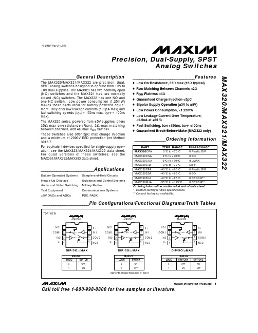
ELECTRICAL CHARACTERISTICS
(V+ = +5V ±10%, V- = -5V ±10%, VINH = 3.5V, VINL = 2.5V, TA = TMIN to TMAX, unless otherwise noted.)
PARAMETER ANALOG SWITCH Analog Signal Range
For equivalent devices specified for single-supply operation, see the MAX323/MAX324/MAX325 data sheet. For quad versions of these switches, see the MAX391/MAX392/MAX393 data sheet.
Plastic DIP (derate 9.09mW/°C above +70°C) .............727mW Narrow SO (derate 5.88mW/°C above +70°C) .............471mW
µMAX (derate 4.10mW/°C above +70°C) .....................330mW CERDIP (derate 8.00mW/°C above +70°C) ..................640mW Operating Temperature Ranges MAX32_C_ _ ........................................................0°C to +70°C MAX32_E_ _......................................................-40°C to +85°C MAX32_MJA ...................................................-55°C to +125°C Storage Temperature Range .............................-65°C to +150°C Lead Temperature (soldering, 10sec) .............................+300°C
- 1、下载文档前请自行甄别文档内容的完整性,平台不提供额外的编辑、内容补充、找答案等附加服务。
- 2、"仅部分预览"的文档,不可在线预览部分如存在完整性等问题,可反馈申请退款(可完整预览的文档不适用该条件!)。
- 3、如文档侵犯您的权益,请联系客服反馈,我们会尽快为您处理(人工客服工作时间:9:00-18:30)。
SUMMARYV CEO = 15V;R SAT = 45m ;I C = 4.5A DESCRIPTIONPackaged in the innovative 2mm x 2mm MLP (Micro Leaded Package)outline,this new 4th generation low saturation transistor offers extremely low on state losses making it ideal for use in DC-DC circuits and various driving and power management functions.Additionally users will also gain several other key benefits :Performance capability equivalent to much larger packages Improved circuit efficiency & power levels Lower package height (nom. 0.9mm)PCB area and device placement savings Reduced component countFEATURES•Low Equivalent On Resistance•Extremely Low Saturation Voltage (100mVmax @1A)•h FE specified up to 12A•I C = 4.5A Continuous Collector Current •2mm x 2mm MLPAPPLICATIONS•DC - DC Converters (FET Drivers)•Charging Circuits •Power switches •Motor controlDEVICE MARKINGSAZXTAM322ISSUE 2 - JUNE 20021MPPS™Miniature Package Power Solutions15V NPN LOW SATURATION TRANSISTOR2mm x 2mm Single MLPunderside viewPINOUT2mm x 2mm MLP(single die)DEVICE REEL TAPE WIDTH QUANTITY PER REEL ZXTAM322TA 7’‘8mm 3000units ZXTAM322TC13’‘8mm10000unitsORDERING INFORMATIONZXTAM322ISSUE 2 - JUNE 20022PARAMETERSYMBOL VALUE UNIT Junction to Ambient (a)R θJA 83°C/W Junction to Ambient (b)R θJA 51°C/W Junction to Ambient (d)R θJA 125°C/W Junction to Ambient (e)R θJA42°C/WTHERMAL RESISTANCENOTES(a) For a single device surface mounted on 10sq cm1oz copper on FR4 PCB in still air conditions with all exposed pads attached .(b) For a single device surface mounted on 10sq cm1oz copper on FR4 PCB in still air conditions measured at t р5 secs with all exposed pads attached.(c) Repetitive rating - pulse width limited by max junction temperature. refer to Transient Thermal Impedance graph.(d) For a single device surface mounted on 10sq cm1oz copper on FR4 PCB in still air conditions with minimal lead connections only .(e) For a single device surface mounted on 65sq cm2oz copper on FR4 PCB in still air conditions with all exposed pads attached .(f) The minimum copper dimensions required for mounting are no smaller than the exposed metal pads on the base of the device, as shown in the package dimensions data. The thermal resistance for a device mounted on 1.5mm thick FR4 board using minimum copper of 1oz weight and 1mm wide track is Rth=300°C/W giving a power rating of Ptot=420mW.PARAMETERSYMBOL LIMIT UNIT Collector-Base Voltage V CBO 40V Collector-Emitter Voltage V CEO 15V Emitter-Base Voltage V EBO 7.5V Peak Pulse Current (c)I CM 15A Continuous Collector Current (a)I C 4.5A Continuous Collector Current (b)I C 5A Base CurrentI B 1000mA Power Dissipation at TA=25°C (a)Linear Derating FactorP D 1.512W mW/°C Power Dissipation at TA=25°C (b)Linear Derating FactorP D 2.4519.6W mW/°C Power Dissipation at TA=25°C (d)Linear Derating FactorP D 18W mW/°C Power Dissipation at TA=25°C (e)Linear Derating FactorP D 324W mW/°C Operating and Storage Temperature RangeT j :T stg-55 to +150°CABSOLUTE MAXIMUM RATINGS.ZXTAM322TYPICAL CHARACTERISTICSISSUE 2 - JUNE 20023ZXTAM322ISSUE 2 - JUNE 20024PARAMETERSYMBOL MIN.TYP .MAX.UNIT CONDITIONS.Collector-Base Breakdown VoltageV (BR)CBO 4070V I C =100A Collector-Emitter Breakdown VoltageV (BR)CEO 1518V I C =10mA*Emitter-Base Breakdown Voltage V (BR)EBO 7.58.2V I E =100A Collector Cut-Off Current I CBO 25nA V CB =32V Emitter Cut-Off CurrentI EBO 25nA V EB =6V Collector Emitter Cut-Off Current I CES 25nA V CES =12VCollector-Emitter Saturation VoltageV CE(sat)87016524020014100200280mV mV mV mV mV I C =0.1A,I B =10mA*I C =1A,I B =10mA*I C =3A,I B =50mA*I C =4.5A,I B =50mA*I C =4.5A,I B =100mA*Base-Emitter Saturation Voltage V BE(sat)0.94 1.0V I C =4.5A,I B =50mA*Base-Emitter Turn-On Voltage V BE(on)0.880.95VI C =4.5A,V CE =2V*Static Forward Current Transfer Ratioh FE20030020015041545032024080I C =10mA,V CE =2V*I C =0.2A,V CE =2V*I C =3A,V CE =2V*I C =5A,V CE =2V*I C =12A,V CE =2V*Transition Frequency f T 80120MHz I C =50mA,V CE =10V f=100MHz Output Capacitance C obo 3040pF V CB =10V,f=1MHz Turn-On Time t (on)120ns V CC =10V,I C =1A I B1=I B2=10mATurn-Off Timet (off)160nsELECTRICAL CHARACTERISTICS (at T amb = 25°C unless otherwise stated).*Measured under pulsed conditions. Pulse width=300µs. Duty cycle ≤2%ISSUE 2 - JUNE 20025ZXTAM322ISSUE 2 - JUNE 20026EuropeZetex plcFields New Road ChaddertonOldham, OL9 8NP United KingdomTelephone (44) 161 622 4422Fax: (44) 161 622 4420uksales@Zetex GmbHStreitfeldstraße 19D-81673 München GermanyTelefon: (49) 89 45 49 49 0Fax: (49) 89 45 49 49 49europe.sales@AmericasZetex Inc700 Veterans Memorial Hwy Hauppauge, NY11788USATelephone: (631) 360 2222Fax: (631) 360 8222usa.sales@Asia PacificZetex (Asia) Ltd3701-04Metroplaza, Tower 1Hing Fong Road Kwai Fong Hong KongTelephone: (852) 26100 611Fax: (852) 24250 494asia.sales@These offices are supported by agents and distributors in major countries world-wide.This publication is issued to provide outline information only which (unless agreed by the Company in writing)may not be used,applied or reproduced for any purpose or form part of any order or contract or be regarded as a representation relating to the products or services concerned.The Company reserves the right to alter without notice the specification,design,price or conditions of supply of any product or service.For the latest product information,log on to©Zetexplc 2002CONTROLLING DIMENSIONS IN MILLIMETRES APPROX. CONVERTED DIMENSIONS IN INCHESMLP322 PACKAGE OUTLINE (2mm x 2mm Micro Leaded Package)DIM MILLIMETRES INCHES DIM MILLIMETRES INCHES MIN.MAX.MIN.MAX.MIN.MAX.MIN.MAX.A 0.80 1.000.03150.0393e 0.65 REF 0.0255 REF A10.000.050.000.002E 2.00 BSC 0.0787 BSC A20.650.750.02550.0295E20.790.990.0310.039A30.150.250.00590.0098E40.480.680.01880.0267b 0.180.280.00700.0110L 0.200.450.00780.0177b10.170.300.00660.0118L20.125 MAX.0.005 REF D 2.00 BSC 0.0787 BSCr 0.075 BSC 0.0029 BSC D2 1.22 1.420.04800.0559⍜0Њ12Њ0Њ12ЊD40.560.760.02200.0299PACKAGE DIMENSIONS分销商库存信息: DIODESZXTAM322TA。