STUS518中文资料
CS5341
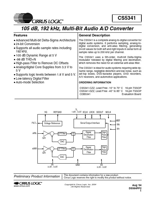
FILT+
Voltage Reference
RST Serial Output Interface
M0
M1
AINL
+
S/H
LP Filter
Q
Digital Decimation
Filter
High Pass Filter
DAC
AINR
+
LP Filter
Q
-
S/H
DAC
Digital Decimation
2 PIN DESCRIPTION ................................................................................................................. 15 3 TYPICAL CONNECTION DIAGRAM ....................................................................................... 16 4 APPLICATIONS ....................................................................................................................... 17
ORDERING INFORMATION
CS5341-CZZ, Lead Free -10° to 70° C 16-pin TSSOP
CS5341-DZZ, Lead Free -40° to 85° C 16-pin TSSOP
CDB5341
1955918资料

Extract from the onlinecatalogCCVA 2,5/ 8-G-5,08 P26THROrder No.: 1955918The figure shows a 10-position version of the producthttp://eshop.phoenixcontact.de/phoenix/treeViewClick.do?UID=1955918Headers, pin length: 2.6 mm, 5.08 mm pitch, 8-pos.http://Please note that the data givenhere has been taken from theonline catalog. For comprehensiveinformation and data, please referto the user documentation. TheGeneral Terms and Conditions ofUse apply to Internet downloads. Technical dataDimensions / positionsPitch 5.08 mmDimension a35.56 mmNumber of positions8Pin dimensions 1 x 1 mmPin spacing 5.08 mmHole diameter 1.6 mmTechnical dataInsulating material group IIIaRated surge voltage (III/3) 4 kVRated surge voltage (III/2) 4 kVRated surge voltage (II/2) 4 kVRated voltage (III/2)320 VRated voltage (II/2)400 VConnection in acc. with standard EN-VDENominal current I N12 ANominal voltage U N250 VMaximum load current12 A (per position)Insulating material LCPInflammability class acc. to UL 94V0Certificates / ApprovalsApproval logoCULNominal voltage U N300 VNominal current I N10 AULNominal voltage U N300 VNominal current I N10 ACertification CUL, ULAccessoriesItem Designation DescriptionGeneral1954362CR-MSTB NAT HT HT coding section, is pushed into the recess on the header beforethe reflow process, made of highly temperature-resistant, beigeinsulating materialMarking1051993B-STIFT Marker pen, for manual labeling of unprinted Zack strips, smear-proof and waterproof, line thickness 0.5 mm0804293SK 5,08/3,8:FORTL.ZAHLEN Marker card, printed horizontally, self-adhesive, 12 identicaldecades marked 1-10, 11-20 etc. up to 91-(99)100, sufficient for120 terminal blocks0805085SK 5,08/3,8:SO Marker card, special printing, self-adhesive, labeled acc. tocustomer requirements, 12 identical marker strips per card, max.25-position labeling per strip, color: white0805412SK 5,08/3,8:UNBEDRUCKT Marker cards, unprinted, with pitch divisions, self-adhesive, 10-section marker strips, 12 strips per card, can be labeled with theM-PENPlug/Adapter1734401CR-MSTB Coding section, inserted into the recess in the header or theinverted plug, red insulating materialDrawingsApplication drawingDrilling diagramDimensioned drawingBottom view, free space for solder paste, 0.55mm deepAddressPHOENIX CONTACT GmbH & Co. KGFlachsmarktstr. 832825 Blomberg,GermanyPhone +49 5235 3 00Fax +49 5235 3 41200http://www.phoenixcontact.de© 2008 Phoenix ContactTechnical modifications reserved;。
SN74LS56P中文资料

Copyright © 1988, Texas Instruments Incorporated PRODUCTION DATA information is current as of publication date.Products conform to specifications per the terms of Texas Instrumentsstandard warranty. Production processing does not necessarily includetesting of all parameters.1POST OFFICE BOX 655303 • DALLAS, TEXAS 752652POST OFFICE BOX 655303 • DALLAS, TEXAS 752653 POST OFFICE BOX 655303 • DALLAS, TEXAS 75265IMPORTANT NOTICETexas Instruments Incorporated and its subsidiaries(TI)reserve the right to make corrections,modifications,enhancements, improvements,and other changes to its products and services at any time and to discontinue any product or service without notice. Customers should obtain the latest relevant information before placing orders and should verify that such information is current and complete.All products are sold subject to TI’s terms and conditions of sale supplied at the time of order acknowledgment.TI warrants performance of its hardware products to the specifications applicable at the time of sale in accordance with TI’s standard warranty.Testing and other quality control techniques are used to the extent TI deems necessary to support this warranty.Except where mandated by government requirements,testing of all parameters of each product is not necessarily performed.TI assumes no liability for applications assistance or customer product design.Customers are responsible for their products and applications using TI components.To minimize the risks associated with customer products and applications,customers should provide adequate design and operating safeguards.TI does not warrant or represent that any license,either express or implied,is granted under any TI patent right,copyright,mask work right,or other TI intellectual property right relating to any combination,machine,or process in which TI products or services are rmation published by TI regarding third-party products or services does not constitute a license from TI to use such products or services or a warranty or endorsement e of such information may require a license from a third party under the patents or other intellectual property of the third party,or a license from TI under the patents or other intellectual property of TI. Reproduction of information in TI data books or data sheets is permissible only if reproduction is without alteration and is accompanied by all associated warranties,conditions,limitations,and notices.Reproduction of this information with alteration is an unfair and deceptive business practice.TI is not responsible or liable for such altered documentation.Resale of TI products or services with statements different from or beyond the parameters stated by TI for that product or service voids all express and any implied warranties for the associated TI product or service and is an unfair and deceptive business practice.TI is not responsible or liable for any such statements.TI products are not authorized for use in safety-critical applications(such as life support)where a failure of the TI product would reasonably be expected to cause severe personal injury or death,unless officers of the parties have executed an agreement specifically governing such use.Buyers represent that they have all necessary expertise in the safety and regulatory ramifications of their applications,and acknowledge and agree that they are solely responsible for all legal,regulatory and safety-related requirements concerning their products and any use of TI products in such safety-critical applications,notwithstanding any applications-related information or support that may be provided by TI.Further,Buyers must fully indemnify TI and its representatives against any damages arising out of the use of TI products in such safety-critical applications.TI products are neither designed nor intended for use in military/aerospace applications or environments unless the TI products are specifically designated by TI as military-grade or"enhanced plastic."Only products designated by TI as military-grade meet military specifications.Buyers acknowledge and agree that any such use of TI products which TI has not designated as military-grade is solely at the Buyer's risk,and that they are solely responsible for compliance with all legal and regulatory requirements in connection with such use.TI products are neither designed nor intended for use in automotive applications or environments unless the specific TI products are designated by TI as compliant with ISO/TS16949requirements.Buyers acknowledge and agree that,if they use anynon-designated products in automotive applications,TI will not be responsible for any failure to meet such requirements. Following are URLs where you can obtain information on other Texas Instruments products and application solutions:Products ApplicationsAmplifiers Audio /audioData Converters Automotive /automotiveDSP Broadband /broadbandInterface Digital Control /digitalcontrolLogic Military /militaryPower Mgmt Optical Networking /opticalnetworkMicrocontrollers Security /securityLow Power /lpw Telephony /telephonyWirelessVideo&Imaging /videoWireless /wirelessMailing Address:Texas Instruments,Post Office Box655303,Dallas,Texas75265Copyright©2007,Texas Instruments IncorporatedIMPORTANT NOTICETexas Instruments Incorporated and its subsidiaries(TI)reserve the right to make corrections,modifications,enhancements, improvements,and other changes to its products and services at any time and to discontinue any product or service without notice. Customers should obtain the latest relevant information before placing orders and should verify that such information is current and complete.All products are sold subject to TI’s terms and conditions of sale supplied at the time of order acknowledgment.TI warrants performance of its hardware products to the specifications applicable at the time of sale in accordance with TI’s standard warranty.Testing and other quality control techniques are used to the extent TI deems necessary to support this warranty.Except where mandated by government requirements,testing of all parameters of each product is not necessarily performed.TI assumes no liability for applications assistance or customer product design.Customers are responsible for their products and applications using TI components.To minimize the risks associated with customer products and applications,customers should provide adequate design and operating safeguards.TI does not warrant or represent that any license,either express or implied,is granted under any TI patent right,copyright,mask work right,or other TI intellectual property right relating to any combination,machine,or process in which TI products or services are rmation published by TI regarding third-party products or services does not constitute a license from TI to use such products or services or a warranty or endorsement e of such information may require a license from a third party under the patents or other intellectual property of the third party,or a license from TI under the patents or other intellectual property of TI. Reproduction of information in TI data books or data sheets is permissible only if reproduction is without alteration and is accompanied by all associated warranties,conditions,limitations,and notices.Reproduction of this information with alteration is an unfair and deceptive business practice.TI is not responsible or liable for such altered documentation.Resale of TI products or services with statements different from or beyond the parameters stated by TI for that product or service voids all express and any implied warranties for the associated TI product or service and is an unfair and deceptive business practice.TI is not responsible or liable for any such statements.TI products are not authorized for use in safety-critical applications(such as life support)where a failure of the TI product would reasonably be expected to cause severe personal injury or death,unless officers of the parties have executed an agreement specifically governing such use.Buyers represent that they have all necessary expertise in the safety and regulatory ramifications of their applications,and acknowledge and agree that they are solely responsible for all legal,regulatory and safety-related requirements concerning their products and any use of TI products in such safety-critical applications,notwithstanding any applications-related information or support that may be provided by TI.Further,Buyers must fully indemnify TI and its representatives against any damages arising out of the use of TI products in such safety-critical applications.TI products are neither designed nor intended for use in military/aerospace applications or environments unless the TI products are specifically designated by TI as military-grade or"enhanced plastic."Only products designated by TI as military-grade meet military specifications.Buyers acknowledge and agree that any such use of TI products which TI has not designated as military-grade is solely at the Buyer's risk,and that they are solely responsible for compliance with all legal and regulatory requirements in connection with such use.TI products are neither designed nor intended for use in automotive applications or environments unless the specific TI products are designated by TI as compliant with ISO/TS16949requirements.Buyers acknowledge and agree that,if they use anynon-designated products in automotive applications,TI will not be responsible for any failure to meet such requirements. Following are URLs where you can obtain information on other Texas Instruments products and application solutions:Products ApplicationsAmplifiers Audio /audioData Converters Automotive /automotiveDSP Broadband /broadbandInterface Digital Control /digitalcontrolLogic Military /militaryPower Mgmt Optical Networking /opticalnetworkMicrocontrollers Security /securityLow Power /lpw Telephony /telephonyWirelessVideo&Imaging /videoWireless /wirelessMailing Address:Texas Instruments,Post Office Box655303,Dallas,Texas75265Copyright©2007,Texas Instruments IncorporatedIMPORTANT NOTICETexas Instruments Incorporated and its subsidiaries(TI)reserve the right to make corrections,modifications,enhancements, improvements,and other changes to its products and services at any time and to discontinue any product or service without notice. Customers should obtain the latest relevant information before placing orders and should verify that such information is current and complete.All products are sold subject to TI’s terms and conditions of sale supplied at the time of order acknowledgment.TI warrants performance of its hardware products to the specifications applicable at the time of sale in accordance with TI’s standard warranty.Testing and other quality control techniques are used to the extent TI deems necessary to support this warranty.Except where mandated by government requirements,testing of all parameters of each product is not necessarily performed.TI assumes no liability for applications assistance or customer product design.Customers are responsible for their products and applications using TI components.To minimize the risks associated with customer products and applications,customers should provide adequate design and operating safeguards.TI does not warrant or represent that any license,either express or implied,is granted under any TI patent right,copyright,mask work right,or other TI intellectual property right relating to any combination,machine,or process in which TI products or services are rmation published by TI regarding third-party products or services does not constitute a license from TI to use such products or services or a warranty or endorsement e of such information may require a license from a third party under the patents or other intellectual property of the third party,or a license from TI under the patents or other intellectual property of TI. Reproduction of information in TI data books or data sheets is permissible only if reproduction is without alteration and is accompanied by all associated warranties,conditions,limitations,and notices.Reproduction of this information with alteration is an unfair and deceptive business practice.TI is not responsible or liable for such altered documentation.Resale of TI products or services with statements different from or beyond the parameters stated by TI for that product or service voids all express and any implied warranties for the associated TI product or service and is an unfair and deceptive business practice.TI is not responsible or liable for any such statements.TI products are not authorized for use in safety-critical applications(such as life support)where a failure of the TI product would reasonably be expected to cause severe personal injury or death,unless officers of the parties have executed an agreement specifically governing such use.Buyers represent that they have all necessary expertise in the safety and regulatory ramifications of their applications,and acknowledge and agree that they are solely responsible for all legal,regulatory and safety-related requirements concerning their products and any use of TI products in such safety-critical applications,notwithstanding any applications-related information or support that may be provided by TI.Further,Buyers must fully indemnify TI and its representatives against any damages arising out of the use of TI products in such safety-critical applications.TI products are neither designed nor intended for use in military/aerospace applications or environments unless the TI products are specifically designated by TI as military-grade or"enhanced plastic."Only products designated by TI as military-grade meet military specifications.Buyers acknowledge and agree that any such use of TI products which TI has not designated as military-grade is solely at the Buyer's risk,and that they are solely responsible for compliance with all legal and regulatory requirements in connection with such use.TI products are neither designed nor intended for use in automotive applications or environments unless the specific TI products are designated by TI as compliant with ISO/TS16949requirements.Buyers acknowledge and agree that,if they use anynon-designated products in automotive applications,TI will not be responsible for any failure to meet such requirements. Following are URLs where you can obtain information on other Texas Instruments products and application solutions:Products ApplicationsAmplifiers Audio /audioData Converters Automotive /automotiveDSP Broadband /broadbandInterface Digital Control /digitalcontrolLogic Military /militaryPower Mgmt Optical Networking /opticalnetworkMicrocontrollers Security /securityLow Power /lpw Telephony /telephonyWirelessVideo&Imaging /videoWireless /wirelessMailing Address:Texas Instruments,Post Office Box655303,Dallas,Texas75265Copyright©2007,Texas Instruments IncorporatedIMPORTANT NOTICETexas Instruments Incorporated and its subsidiaries(TI)reserve the right to make corrections,modifications,enhancements, improvements,and other changes to its products and services at any time and to discontinue any product or service without notice. Customers should obtain the latest relevant information before placing orders and should verify that such information is current and complete.All products are sold subject to TI’s terms and conditions of sale supplied at the time of order acknowledgment.TI warrants performance of its hardware products to the specifications applicable at the time of sale in accordance with TI’s standard warranty.Testing and other quality control techniques are used to the extent TI deems necessary to support this warranty.Except where mandated by government requirements,testing of all parameters of each product is not necessarily performed.TI assumes no liability for applications assistance or customer product design.Customers are responsible for their products and applications using TI components.To minimize the risks associated with customer products and applications,customers should provide adequate design and operating safeguards.TI does not warrant or represent that any license,either express or implied,is granted under any TI patent right,copyright,mask work right,or other TI intellectual property right relating to any combination,machine,or process in which TI products or services are rmation published by TI regarding third-party products or services does not constitute a license from TI to use such products or services or a warranty or endorsement e of such information may require a license from a third party under the patents or other intellectual property of the third party,or a license from TI under the patents or other intellectual property of TI. Reproduction of information in TI data books or data sheets is permissible only if reproduction is without alteration and is accompanied by all associated warranties,conditions,limitations,and notices.Reproduction of this information with alteration is an unfair and deceptive business practice.TI is not responsible or liable for such altered documentation.Resale of TI products or services with statements different from or beyond the parameters stated by TI for that product or service voids all express and any implied warranties for the associated TI product or service and is an unfair and deceptive business practice.TI is not responsible or liable for any such statements.TI products are not authorized for use in safety-critical applications(such as life support)where a failure of the TI product would reasonably be expected to cause severe personal injury or death,unless officers of the parties have executed an agreement specifically governing such use.Buyers represent that they have all necessary expertise in the safety and regulatory ramifications of their applications,and acknowledge and agree that they are solely responsible for all legal,regulatory and safety-related requirements concerning their products and any use of TI products in such safety-critical applications,notwithstanding any applications-related information or support that may be provided by TI.Further,Buyers must fully indemnify TI and its representatives against any damages arising out of the use of TI products in such safety-critical applications.TI products are neither designed nor intended for use in military/aerospace applications or environments unless the TI products are specifically designated by TI as military-grade or"enhanced plastic."Only products designated by TI as military-grade meet military specifications.Buyers acknowledge and agree that any such use of TI products which TI has not designated as military-grade is solely at the Buyer's risk,and that they are solely responsible for compliance with all legal and regulatory requirements in connection with such use.TI products are neither designed nor intended for use in automotive applications or environments unless the specific TI products are designated by TI as compliant with ISO/TS16949requirements.Buyers acknowledge and agree that,if they use anynon-designated products in automotive applications,TI will not be responsible for any failure to meet such requirements. Following are URLs where you can obtain information on other Texas Instruments products and application solutions:Products ApplicationsAmplifiers Audio /audioData Converters Automotive /automotiveDSP Broadband /broadbandInterface Digital Control /digitalcontrolLogic Military /militaryPower Mgmt Optical Networking /opticalnetworkMicrocontrollers Security /securityLow Power /lpw Telephony /telephonyWirelessVideo&Imaging /videoWireless /wirelessMailing Address:Texas Instruments,Post Office Box655303,Dallas,Texas75265Copyright©2007,Texas Instruments IncorporatedIMPORTANT NOTICETexas Instruments Incorporated and its subsidiaries(TI)reserve the right to make corrections,modifications,enhancements, improvements,and other changes to its products and services at any time and to discontinue any product or service without notice. Customers should obtain the latest relevant information before placing orders and should verify that such information is current and complete.All products are sold subject to TI’s terms and conditions of sale supplied at the time of order acknowledgment.TI warrants performance of its hardware products to the specifications applicable at the time of sale in accordance with TI’s standard warranty.Testing and other quality control techniques are used to the extent TI deems necessary to support this warranty.Except where mandated by government requirements,testing of all parameters of each product is not necessarily performed.TI assumes no liability for applications assistance or customer product design.Customers are responsible for their products and applications using TI components.To minimize the risks associated with customer products and applications,customers should provide adequate design and operating safeguards.TI does not warrant or represent that any license,either express or implied,is granted under any TI patent right,copyright,mask work right,or other TI intellectual property right relating to any combination,machine,or process in which TI products or services are rmation published by TI regarding third-party products or services does not constitute a license from TI to use such products or services or a warranty or endorsement e of such information may require a license from a third party under the patents or other intellectual property of the third party,or a license from TI under the patents or other intellectual property of TI. Reproduction of information in TI data books or data sheets is permissible only if reproduction is without alteration and is accompanied by all associated warranties,conditions,limitations,and notices.Reproduction of this information with alteration is an unfair and deceptive business practice.TI is not responsible or liable for such altered documentation.Resale of TI products or services with statements different from or beyond the parameters stated by TI for that product or service voids all express and any implied warranties for the associated TI product or service and is an unfair and deceptive business practice.TI is not responsible or liable for any such statements.TI products are not authorized for use in safety-critical applications(such as life support)where a failure of the TI product would reasonably be expected to cause severe personal injury or death,unless officers of the parties have executed an agreement specifically governing such use.Buyers represent that they have all necessary expertise in the safety and regulatory ramifications of their applications,and acknowledge and agree that they are solely responsible for all legal,regulatory and safety-related requirements concerning their products and any use of TI products in such safety-critical applications,notwithstanding any applications-related information or support that may be provided by TI.Further,Buyers must fully indemnify TI and its representatives against any damages arising out of the use of TI products in such safety-critical applications.TI products are neither designed nor intended for use in military/aerospace applications or environments unless the TI products are specifically designated by TI as military-grade or"enhanced plastic."Only products designated by TI as military-grade meet military specifications.Buyers acknowledge and agree that any such use of TI products which TI has not designated as military-grade is solely at the Buyer's risk,and that they are solely responsible for compliance with all legal and regulatory requirements in connection with such use.TI products are neither designed nor intended for use in automotive applications or environments unless the specific TI products are designated by TI as compliant with ISO/TS16949requirements.Buyers acknowledge and agree that,if they use anynon-designated products in automotive applications,TI will not be responsible for any failure to meet such requirements. Following are URLs where you can obtain information on other Texas Instruments products and application solutions:Products ApplicationsAmplifiers Audio /audioData Converters Automotive /automotiveDSP Broadband /broadbandInterface Digital Control /digitalcontrolLogic Military /militaryPower Mgmt Optical Networking /opticalnetworkMicrocontrollers Security /securityLow Power /lpw Telephony /telephonyWirelessVideo&Imaging /videoWireless /wirelessMailing Address:Texas Instruments,Post Office Box655303,Dallas,Texas75265Copyright©2007,Texas Instruments IncorporatedIMPORTANT NOTICETexas Instruments Incorporated and its subsidiaries(TI)reserve the right to make corrections,modifications,enhancements, improvements,and other changes to its products and services at any time and to discontinue any product or service without notice. Customers should obtain the latest relevant information before placing orders and should verify that such information is current and complete.All products are sold subject to TI’s terms and conditions of sale supplied at the time of order acknowledgment.TI warrants performance of its hardware products to the specifications applicable at the time of sale in accordance with TI’s standard warranty.Testing and other quality control techniques are used to the extent TI deems necessary to support this warranty.Except where mandated by government requirements,testing of all parameters of each product is not necessarily performed.TI assumes no liability for applications assistance or customer product design.Customers are responsible for their products and applications using TI components.To minimize the risks associated with customer products and applications,customers should provide adequate design and operating safeguards.TI does not warrant or represent that any license,either express or implied,is granted under any TI patent right,copyright,mask work right,or other TI intellectual property right relating to any combination,machine,or process in which TI products or services are rmation published by TI regarding third-party products or services does not constitute a license from TI to use such products or services or a warranty or endorsement e of such information may require a license from a third party under the patents or other intellectual property of the third party,or a license from TI under the patents or other intellectual property of TI. Reproduction of information in TI data books or data sheets is permissible only if reproduction is without alteration and is accompanied by all associated warranties,conditions,limitations,and notices.Reproduction of this information with alteration is an unfair and deceptive business practice.TI is not responsible or liable for such altered documentation.Resale of TI products or services with statements different from or beyond the parameters stated by TI for that product or service voids all express and any implied warranties for the associated TI product or service and is an unfair and deceptive business practice.TI is not responsible or liable for any such statements.TI products are not authorized for use in safety-critical applications(such as life support)where a failure of the TI product would reasonably be expected to cause severe personal injury or death,unless officers of the parties have executed an agreement specifically governing such use.Buyers represent that they have all necessary expertise in the safety and regulatory ramifications of their applications,and acknowledge and agree that they are solely responsible for all legal,regulatory and safety-related requirements concerning their products and any use of TI products in such safety-critical applications,notwithstanding any applications-related information or support that may be provided by TI.Further,Buyers must fully indemnify TI and its representatives against any damages arising out of the use of TI products in such safety-critical applications.TI products are neither designed nor intended for use in military/aerospace applications or environments unless the TI products are specifically designated by TI as military-grade or"enhanced plastic."Only products designated by TI as military-grade meet military specifications.Buyers acknowledge and agree that any such use of TI products which TI has not designated as military-grade is solely at the Buyer's risk,and that they are solely responsible for compliance with all legal and regulatory requirements in connection with such use.TI products are neither designed nor intended for use in automotive applications or environments unless the specific TI products are designated by TI as compliant with ISO/TS16949requirements.Buyers acknowledge and agree that,if they use anynon-designated products in automotive applications,TI will not be responsible for any failure to meet such requirements. Following are URLs where you can obtain information on other Texas Instruments products and application solutions:Products ApplicationsAmplifiers Audio /audioData Converters Automotive /automotiveDSP Broadband /broadbandInterface Digital Control /digitalcontrolLogic Military /militaryPower Mgmt Optical Networking /opticalnetworkMicrocontrollers Security /securityLow Power /lpw Telephony /telephonyWirelessVideo&Imaging /videoWireless /wirelessMailing Address:Texas Instruments,Post Office Box655303,Dallas,Texas75265Copyright©2007,Texas Instruments Incorporated。
at89s51中文资料_数据手册_参数
XTAL2 10 XTAL1 11
GND 12 PWRGND 13 (A8) P2.0 14 (A9) P2.1 15 (A10) P2.2 16 (A11) P2.3 17 (A12) P2.4 18 (A13) P2.5 19 (A14) P2.6 20 (A15) P2.7 21
The AT89S51 provides the following standard features: 4K bytes of Flash, 128 bytes of RAM, 32 I/O lines, Watchdog timer, two data pointers, two 16-bit timer/counters, a five-vector two-level interrupt architecture, a full duplex serial port, on-chip oscillator, and clock circuitry. In addition, the AT89S51 is designed with static logic for operation down to zero frequency and supports two software selectable power saving modes. The Idle Mode stops the CPU while allowing the RAM, timer/counters, serial port, and interrupt system to continue functioning. The Power-down mode saves the RAM contents but freezes the oscillator, disabling all other chip functions until the next external interrupt or hardware reset.
ABB机器人操作手册(中文版)
3HAC16590-10 米Ι : N
3
© Copyright 2004-2010 ABB. 保留所有权利。
目表
3.3.6 备份和恢复 . . . . . . . . . . . . . . . . . . . . . . . . . . . . . . . . . 69 3.3.7 在生产模式下运行 . . . . . . . . . . . . . . . . . . . . . . . . . . . . . . 70 3.3.8 授予 RobotStudio 访问权限 . . . . . . . . . . . . . . . . . . . . . . . . . 71 3.3.9 升级 . . . . . . . . . . . . . . . . . . . . . . . . . . . . . . . . . . . . 72 3.3.10 安装软件选项 . . . . . . . . . . . . . . . . . . . . . . . . . . . . . . . 73 3.3.11 关闭 . . . . . . . . . . . . . . . . . . . . . . . . . . . . . . . . . . . 74
1.4 如何处理紧急情况 . . . . . . . . . . . . . . . . . . . . . . . . . . . . . . . . . . . . . 32 1.4.1 停止系统 . . . . . . . . . . . . . . . . . . . . . . . . . . . . . . . . . 32 1.4.2 释放机器人制动闸 . . . . . . . . . . . . . . . . . . . . . . . . . . . . . 34 1.4.3 灭火 . . . . . . . . . . . . . . . . . . . . . . . . . . . . . . . . . . . 35 1.4.4 从紧急停止状态恢复 . . . . . . . . . . . . . . . . . . . . . . . . . . . . 36 1.4.5 返回到编程路径 . . . . . . . . . . . . . . . . . . . . . . . . . . . . . . 37
89s52中文资料 通用版
单片机AT89S52中文资料2007-04-05 10:37AT89S521主要性能l 与MCS-51单片机产品兼容l 8K字节在系统可编程Flash存储器l 1000次擦写周期l 全静态操作:0Hz~33MHzl 三级加密程序存储器l 32个可编程I/O口线l 三个16位定时器/计数器l 八个中断源l 全双工UART串行通道l 低功耗空闲和掉电模式l 掉电后中断可唤醒l 看门狗定时器l 双数据指针l 掉电标识符功能特性描述AT89S52是一种低功耗、高性能CMOS8位微控制器,具有8K 在系统可编程Flash 存储器。
使用Atmel 公司高密度非易失性存储器技术制造,与工业80C51 产品指令和引脚完全兼容。
片上Flash允许程序存储器在系统可编程,亦适于常规编程器。
在单芯片上,拥有灵巧的8 位CPU 和在系统可编程Flash,使得AT89S52为众多嵌入式控制应用系统提供高灵活、超有效的解决方案。
AT89S52具有以下标准功能: 8k字节Flash,256字节RAM,32 位I/O 口线,看门狗定时器,2 个数据指针,三个16 位定时器/计数器,一个6向量2级中断结构,全双工串行口,片内晶振及时钟电路。
另外,AT89S52 可降至0Hz 静态逻辑操作,支持2种软件可选择节电模式。
空闲模式下,CPU停止工作,允许RAM、定时器/计数器、串口、中断继续工作。
掉电保护方式下,RAM内容被保存,振荡器被冻结,单片机一切工作停止,直到下一个中断或硬件复位为止。
R8 位微控制器8K 字节在系统可编程FlashAT89S52Rev. 1919-07/01AT89S522引脚结构AT89S523方框图引脚功能描述AT89S524VCC : 电源GND: 地P0 口:P0口是一个8位漏极开路的双向I/O口。
作为输出口,每位能驱动8个TTL逻辑电平。
对P0端口写“1”时,引脚用作高阻抗输入。
当访问外部程序和数据存储器时,P0口也被作为低8位地址/数据复用。
AK5365中文资料

ASAHI KASEI[AK5365]GENERAL DESCRIPTIONAK5365 is a high-performance 24-bit, 96kHz sampling ADC for consumer audio and digital recording applications. Thanks to AKM’s Enhanced Dual-Bit modulator architecture, this analog-to-digital converter has an impressive dynamic range of 103dB with a high level of integration. The AK5365 has a 5-channel stereo input selector, an input Programmable Gain Amplifier with an ALC function. All this integration with high-performance makes the AK5365 well suited for CD and DVD recording systems.FEATURES1. 24bit Stereo ADC• 5ch Stereo Inputs Selector• Input PGA from +12dB to 0dB, 0.5dB Step• Auto Level Control (ALC) Circuit• Digital HPF for offset cancellation (fc=1.0Hz@fs=48kHz)• Digital Attenuator• Soft Mute• Single-end Inputs• S/(N+D) : 94dB• DR, S/N : 103dB• Audio I/F Format : 24bit MSB justified, I2S2. 3-wire Serial µP Interface / I2C-Bus3. Master / Slave Mode4. Master Clock : 256fs/384fs/512fs5. Sampling Rate : 32kHz to 96kHz6. Power Supply• AVDD: 4.75 ∼ 5.25V (typ. 5.0V)• DVDD: 3.0 ∼ 5.25V (typ. 3.3V)7. Power Supply Current : 27mA8. Ta = -40 ∼85°C9. Package : 44pin LQFPOrdering GuideAK5365VQ −40 ∼ +85°C 44pin LQFP (0.8mm pitch)AKD5365Evaluation Board for AK5365Pin LayoutLIN5R I N 54443142414039383736353433323130292827262524232221201918171615141312234567891011AK5365VQTop ViewTEST1LIN4TEST2LIN3TEST3LIN2TEST4LIN1LOPIN LOUTI P G A LI P G A RR O U TR O P I NA V D DA V S SV C O MD V S SD V D DS D T OB IC K LRCKMCLK PDN ALC SMUTE SEL0SEL1SEL2CDTI/SDA CCLK/SCL CSN/CAD1T E S T 8R I N 4T E S T 7R I N 3T E S T 6R I N 2T E S T 5R I N 1M /SC T R LPIN/FUNCTIONNo.Pin Name I/O Function 1LIN5I Lch Analog Input 5 Pin2TEST1I Test 1 Pin (Connected to AVSS)3LIN4I Lch Analog Input 4 Pin4TEST2I Test 2 Pin (Connected to AVSS)5LIN3I Lch Analog Input 3 Pin6TEST3I Test 3 Pin (Connected to AVSS)7LIN2I Lch Analog Input 2 Pin8TEST4I Test 4 Pin (Connected to AVSS)9LIN1I Lch Analog Input 1 Pin10LOPIN I Lch Feed Back Resistor Input Pin11LOUT O Lch Feed Back Resistor Output Pin12IPGAL I Lch IPGA Input Pin13IPGAR I Rch IPGA Input Pin14ROUT O Rch Feed Back Resistor Output Pin15ROPIN I Rch Feed Back Resistor Input Pin16AVDD-Analog Power Supply Pin, 4.75 ∼ 5.25V17AVSS-Analog Ground Pin18VCOM O Common Voltage Output Pin, AVDD/2 Bias voltage of ADC input.19DVSS-Digital Ground Pin20DVDD-Digital Power Supply Pin, 3.0 ∼ 5.25V21SDTO O Audio Serial Data Output Pin22BICK I/O Audio Serial Data Clock PinNote: All digital input pins except pull-down pins should not be left floating. Note: TEST1, TEST2, TEST3 and TEST4 pins should be connected to AVSS.No.Pin Name I/O Function 23LRCK I/O Output Channel Clock Pin24MCLK I Master Clock Input Pin25PDN I Power-Down Mode Pin“H”: Power up, “L”: Power down reset and initializes the control register.26ALC I ALC Enable Pin (Internal Pull-down Pin, typ. 100kΩ) “H” : ALC Enable, “L” : ALC Disable27SMUTE I Soft Mute Pin (Internal Pull-down Pin, typ. 100kΩ) “H” : Soft Mute, “L” : Normal Operation28SEL0I Input Selector 0 Pin29SEL1I Input Selector 1 Pin30SEL2I Input Selector 2 PinCDTI I Control Data Input Pin in 3-wire Control (CTRL pin = “L”) 31SDA I/O Control Data Input / Output Pin in I2C Control (CTRL pin = “H”)CCLK I Control Data Clock Pin in 3-wire Control (CTRL pin = “L”) 32SCL I Control Data Clock Pin in I2C Control (CTRL pin = “H”)CSN I Chip Select Pin in 3-wire Control (CTRL pin = “L”) 33CAD1I Chip Address 1 Select Pin in I2C Control (CTRL pin = “H”)34CTRL I Control Mode Pin“H” : I2C Control & I2S Compatible, “L” : 3-wire Control35M/S I Master / Slave Mode Pin“H” : Master Mode, “L” : Slave Mode36RIN1I Rch Analog Input 1 Pin37TEST5I Test 5 Pin (Connected to AVSS)38RIN2I Rch Analog Input 2 Pin39TEST6I Test 6 Pin (Connected to AVSS)40RIN3I Rch Analog Input 3 Pin41TEST7I Test 7 Pin (Connected to AVSS)42RIN4I Rch Analog Input 4 Pin43TEST8I Test 8 Pin (Connected to AVSS)44RIN5I Rch Analog Input 5 PinNote: All digital input pins except pull-down pins should not be left floating. Note: TEST5, TEST6, TEST7 and TEST8 pins should be connected to AVSS.ABSOLUTE MAXIMUM RATINGS(AVSS, DVSS=0V; Note 1)Parameter Symbol min max UnitsPower Supplies:AnalogDigital|AVSS – DVSS| (Note 2)AVDDDVDD∆GND−0.3−0.3-6.06.00.3VVVInput Current, Any Pin Except Supplies IIN-±10mA Analog Input Voltage(VREF, LIN1-5, RIN1-5, LOPIN, ROPIN, IPGAL, IPGAR pins)VINA−0.3AVDD+0.3V Digital Input Voltage (All digital input pins)VIND−0.3DVDD+0.3V Ambient Temperature (powered applied)Ta−4085°C Storage Temperature Tstg−65150°C Note 1. All voltages with respect to ground.Note 2. AVSS and DVSS must be connected to the same analog ground plane.WARNING: Operation at or beyond these limits may result in permanent damage to the device.Normal operation is not guaranteed at these extremes.RECOMMENDED OPERATING CONDITIONS(AVSS, DVSS=0V; Note 1)Parameter Symbol min typ max UnitsPower Supplies (Note 3)AnalogDigitalAVDDDVDD4.753.05.03.35.25AVDDVVNote 1. All voltages with respect to ground.Note 3. The power up sequence between AVDD and DVDD is not critical.WARNING: AKM assumes no responsibility for the usage beyond the conditions in this datasheet.ANALOG CHARACTERISTICS(Ta=25°C; AVDD=5.0V, DVDD=3.3V; AVSS=DVSS=0V; fs=48kHz, 96kHz; BICK=64fs; Signal Frequency=1kHz; 24bit Data; Measurement frequency=20Hz ∼ 20kHz at fs=48kHz, 40Hz ∼ 40kHz at fs=96kHz; unless otherwise specified) Parameter min typ max Units Pre-Amp Characteristics:Feedback Resistance1050kΩS/(N+D) (Note 4)-100dBS/N (A-weighted)-108dB Load Resistance (Note 5) 6.3kΩLoad Capacitance20pF Input PGA Characteristics:Input Voltage (Note 6)0.91 1.1Vrms Input Resistance (Note 7) 6.31015kΩStep Size0.20.50.8dBGain Control Range ALC = OFFALC = ON−9.5+12+12dBdBADC Analog Input Characteristics: IPGA=0dB, ALC = OFF (Note 8)Resolution24BitsS/(N+D) (−0.5dBFS)fs=48kHzfs=96kHz 84829492dBdBDR (−60dBFS)fs=48kHz, A-weightedfs=96kHz 968910399dBdBS/N fs=48kHz, A-weightedfs=96kHz 968910399dBdBInterchannel Isolation (Note 9)90110dB Interchannel Gain Mismatch0.20.5dB Gain Drift100-ppm/°C Power Supply Rejection (Note 10)50-dB Power SuppliesPower Supply CurrentNormal Operation (PDN pin = “H”)AVDDDVDD (fs=48kHz)(fs=96kHz)Power-down mode (PDN pin = “L”) (Note 11) AVDDDVDD 2348101035816100100mAmAmAµAµANote 4. This value is measured at LOUT and ROUT pins using the circuit as shown in Figure 24.The input signal voltage is 2Vrms.Note 5. This value is the input impedance of an external device that the LOUT and ROUT pins can drive, when a device is connected with LOUT and ROUT pin externally. The feedback resistor (min. 10kΩ) that it is usually connected with the LOUT/ROUT pins, and the value of input impedance (min. 6.3kΩ) of the IPGAL/R pins are not included. Note 6. Full scale (0dB) of the input voltage at ALC=OFF and IPGA=0dB.Input voltage to IPGAL and IPGAR pins is proportional to AVDD voltage. Vin = 0.2 x AVDD (Vrms).Note 7. This value is input impedance of the IPGAL and IPGAR pins.Note 8. This value is measured via the following path. Pre-Amp → IPGA (Gain : 0dB) → ADC.The measurement circuit is Figure 24.Note 9. This value is the interchannel isolation between all the channels of the LIN1-5 and RIN1-5 when the applied input signal causes the Pre-Amp output to equal IPGA input.Note 10. PSR is applied to AVDD and DVDD with 1kHz, 50mVpp.Note 11. All digital input pins are held DVDD or DVSS.FILTER CHARACTERISTICS (fs=48kHz)(Ta=−40 ∼ 85°C; AVDD=4.75 ∼ 5.25V; DVDD=3.0 ∼ 5.25V; fs=48kHz)Parameter Symbol min typ max Units ADC Digital Filter (Decimation LPF):Passband (Note 12)−0.005dB−0.02dB−0.06dB−6.0dB PB0---21.76822.024.021.5---kHzkHzkHzkHzStopband SB26.5kHz Passband Ripple PR±0.005dB Stopband Attenuation SA80dB Group Delay (Note 13)GD29.61/fs Group Delay Distortion∆GD0µs ADC Digital Filter (HPF):Frequency Response (Note 12)−3dB−0.5dB−0.1dB FR 1.02.96.5HzHzHzNote 12. The passband and stopband frequencies scale with fs. For example, 21.768kHz at −0.02dB is 0.454 x fs. Note 13. The calculated delay time induced by digital filtering. This time is from the input of an analog signalto the setting of 24bit data both channels to the ADC output register for ADC.FILTER CHARACTERISTICS (fs=96kHz)(Ta=−40 ∼ 85°C; AVDD=4.75 ∼ 5.25V; DVDD=3.0 ∼ 5.25V; fs=96kHz)Parameter Symbol min typ max Units ADC Digital Filter (Decimation LPF):Passband (Note 14)−0.005dB−0.02dB−0.06dB−6.0dB PB0---43.53644.048.043.0---kHzkHzkHzkHzStopband SB53.0kHz Passband Ripple PR±0.005dB Stopband Attenuation SA80dB Group Delay (Note 15)GD29.61/fs Group Delay Distortion∆GD0µs ADC Digital Filter (HPF):Frequency Response (Note 14)−3dB−0.5dB−0.1dB FR25.813HzHzHzNote 14. The passband and stopband frequencies scale with fs. For example, 43.536kHz at −0.02dB is 0.454 x fs. Note 15. The calculated delay time induced by digital filtering. This time is from the input of an analog signalto the setting of 24bit data both channels to the ADC output register for ADC.DC CHARACTERISTICS(Ta=−40 ∼ 85°C; AVDD=4.75 ∼ 5.25V; DVDD=3.0 ∼ 5.25V)Parameter Symbol min typ Max UnitsHigh-Level Input Voltage Low-Level Input Voltage VIHVIL70%DVDD----30%DVDDVVHigh-Level Output Voltage (Iout=−400µA) Low-Level Output Voltage(Except SDA pin : Iout=400µA) (SDA pin : Iout=3mA)VOHVOLVOLDVDD-0.5------0.50.4VVVInput Leakage Current Iin--±10µASWITCHING CHARACTERISTICS(Ta=−40 ∼ 85°C; AVDD=4.75 ∼ 5.25V; DVDD=3.0 ∼ 5.25V; C L=20pF)Parameter Symbol min typ max Units Master Clock TimingFrequencyPulse Width Low Pulse Width HighfCLKtCLKLtCLKH8.1920.4/fCLK0.4/fCLK24.576MHznsnsLRCK FrequencyNormal Speed Mode Double Speed Mode fsnfsd32484896kHzkHzDuty Cycle Slave modeMaster mode 455055%%Audio Interface Timing Slave modeBICK PeriodBICK Pulse Width LowPulse Width HighLRCK Edge to BICK “↑” (Note 16) BICK “↑” to LRCK Edge (Note 16) LRCK to SDTO (MSB) (Except I2S mode) BICK “↓” to SDTOtBCKtBCKLtBCKHtLRBtBLRtLRStBSD160656530303535nsnsnsnsnsnsnsMaster modeBICK Frequency BICK DutyBICK “↓” to LRCK BICK “↓” to SDTOfBCKdBCKtMBLRtBSD−20−2064fs502035Hz%nsnsNote 17. BICK rising edge must not occur at the same time as LRCK edge.Parameter Symbol min typ max Units Control Interface Timing (3-wire Serial mode):CCLK PeriodCCLK Pulse Width Low Pulse Width High CDTI Setup TimeCDTI Hold TimeCSN “H” TimeCSN “↓” to CCLK “↑” CCLK “↑” to CSN “↑”tCCKtCCKLtCCKHtCDStCDHtCSWtCSStCSH200808040401505050nsnsnsnsnsnsnsnsControl Interface Timing (I2C Bus mode):SCL Clock FrequencyBus Free Time Between TransmissionsStart Condition Hold Time (prior to first clock pulse) Clock Low TimeClock High TimeSetup Time for Repeated Start ConditionSDA Hold Time from SCL Falling (Note 17) SDA Setup Time from SCL RisingRise Time of Both SDA and SCL LinesFall Time of Both SDA and SCL LinesSetup Time for Stop ConditionPulse Width of Spike Noise Suppressed by Input FilterfSCLtBUFtHD:STAtLOWtHIGHtSU:STAtHD:DATtSU:DATtRtFtSU:STOtSP-4.74.04.74.04.70.25--4.0100-------1.00.3-50kHzµsµsµsµsµsµsµsµsµsµsnsReset TimingPDN Pulse Width (Note 18) PDN “↑” to SDTO valid (Note 19) PWN “↑” to SDTO valid (Note 20)tPDtPDVtPDV150516516ns1/fs1/fsNote 17. Data must be held long enough to bridge the 300ns-transition time of SCL.Note 18. The AK5365 can be reset by bringing the PDN pin = “L”.Note 19. This cycle is the number of LRCK rising edges from the PDN pin = “H”.Note 20. This cycle is the number of LRCK rising edges from the PWN bit = “1”.Purchase of Asahi Kasei Microsystems Co., Ltd I2C components conveys a license under the Philips I2C patent to use the components in the I2C system, provided the system conform to the I2C specifications defined by Philips.Timing DiagramMCLKLRCKBICKClock TimingLRCK VIH VILBICK VIH VILSDTO50%DVDDAudio Interface Timing (Slave mode)LRCK BICK50%DVDDSDTO 50%DVDD50%DVDDAudio Interface Timing (Master mode)CSNVIH VILCCLKVIH VILCDTIVIH VILWRITE Command Input TimingCSNVIH VILCCLKVIH VIL CDTI VIH VILWRITE Data Input TimingSDASCLVILVIL I C Bus Mode TimingPDNVILCSNVIH VILSDTO50%DVDDPDNVIH VILSDTO50%DVDDPower Down & Reset TimingOPERATION OVERVIEWSystem ClockMCLK (256fs/384fs/512fs), BICK (48fs∼) and LRCK (fs) clocks are required in slave mode. The LRCK clock input must be synchronized with MCLK, however the phase is not critical. MCLK frequency is automatically detected in slave mode. Table 1 shows the relationship of typical sampling frequency and the system clock frequency.MCLK (256fs/384fs/512fs) is required in master mode. MCLK frequency is selected by CKS1-0 bits as shown in Table 2. In master mode, after setting CKS1-0 bits, there is a possibility the frequency and duty of LRCK and BICK outputs become an abnormal state.All external clocks (MCLK, BICK and LRCK) must be present unless PDN pin = “L” and PWN bit = “1”. If these clocks are not provided, the AK5365 may draw excess current due to its use of internal dynamically refreshed logic. If the external clocks are not present, place the AK5365 in power-down mode (PDN pin = “L” or PWN bit = “0”). In master mode, the master clock (MCLK) must be provided unless PDN pin = “L”.MCLKfs256fs384fs512fs32kHz8.192MHz12.288MHz16.384MHz44.1kHz11.2896MHz16.9344MHz22.5792MHz48kHz12.288MHz18.432MHz24.576MHz96kHz24.576MHz N/A N/ATable 1. System clock example (Slave mode)MCLKCKS1CKS032kHz ≤ fs ≤ 48kHz48kHz < fs ≤ 96kHz00256fs256fs Default01512fs N/A10384fs N/A11N/A N/ATable 2. Master clock frequency select (Master mode)Audio Interface FormatTwo kinds of data formats can be chosen with the DIF bit (Table 3) and the CTRL pin (Table 4). The DIF bit and CTRL pin are ORed between pin and register. In both modes, the serial data is in MSB first, 2’s compliment format. The SDTO is clocked out on the falling edge of BICK. The audio interface supports both master and slave modes. In master mode, BICK and LRCK are output with the BICK frequency fixed to 64fs and the LRCK frequency fixed to 1fs.Mode DIF bit SDTO LRCK BICK FigureDefault0024bit, MSB justified H/L≥ 48fs Figure 11124bit, I2S Compatible L/H≥ 48fs Figure 2Table 3. Audio Interface Format (CTRL pin = “L”)Mode CTRL pin SDTO LRCK BICK Figure0L24bit, MSB justified H/L≥ 48fs Figure 11H24bit, I2S Compatible L/H≥ 48fs Figure 2Table 4. Audio Interface Format (DIF bit = “0”)LRCKBICK(64fs)SDTO(o)Figure 1. Mode 0 TimingLRCKBICK(64fs)SDTO(o)Figure 2. Mode 1 TimingMaster Mode and Slave ModeThe M/S pin selects either master or slave mode. M/S pin = “H” selects master mode and “L” selects slave mode. The AK5365 outputs BICK and LRCK in master mode. In slave mode, MCLK, BICK and LRCK are input externally.BICK, LRCKSlave Mode BICK = Input LRCK = InputMaster Mode BICK = Output LRCK = OutputTable 5. Master mode/Slave modeDigital High Pass FilterThe ADC has a digital high pass filter for DC offset cancellation. The cut-off frequency of the HPF is 1.0Hz (@fs=48kHz) and scales with sampling rate (fs).Power-up/downThe AK5365 is placed in the power-down mode by bringing PDN pin = “L” and the digital filter is also reset at the same time. This reset should always be done after power-up. An analog initialization cycle starts after exiting the power-down mode. Therefore, the output data SDTO becomes available after 516 cycles of LRCK.(1) Power-up Sequence 1Power SupplyPDN pinADC Internal StateIPGASDTOExternal clocksin slave modeExternal clocksin master modeBICK, LRCKin master mode- INITA :Initializing period of ADC analog section (516/fs).- FI :Fade in. After exiting power down, IPGA value fades in.- PDN :Power down state.- The period of (1) should be min. 150ns in Figure 3.Figure 3. Power-up Sequence 1(2) Power-up Sequence 2Power SupplyPDN pinADC Internal StateIPGASDTOExternal clocksin slave modeExternal clocksin master modeBICK, LRCKin master mode- INITA :Initializing period of ADC analog section (516/fs).- FI :Fade in. After exiting power down, IPGA value fades in.- PDN :Power down state.- The period of (1) should be min. 150ns in Figure 4.Figure 4. Power-up Sequence 2Input SelectorThe AK5365 includes 5ch stereo input selectors (Figure 5). The input selector is 5 to 1 selector. The input channel is set by the SEL2-0 bits (Table 6) and the SEL2-0 pins (Table 7). The SEL2-0 pins should be fixed to “LLL” if the AK5365 is controlled by the SEL 2-0 bits, because the setting of the SEL2-0 pins are prior to the SEL2-0 bits setting.SEL2 bit SEL1 bit SEL0 bit Input Channel000LIN1 / RIN1Default001LIN2 / RIN2010LIN3 / RIN3011LIN4 / RIN4100LIN5 / RIN5Table 6. Input Selector (SEL2-0 pin = “LLL”)SEL2 pin SEL1 pin SEL0 pin Input ChannelL L L LIN1 / RIN1L L H LIN2 / RIN2L H L LIN3 / RIN3L H H LIN4 / RIN4H L L LIN5 / RIN5Table 7. Input Selector (SEL2-0 bit = “000”)Figure 5. Input Selector[Input selector switching sequence]The input selector should be changed after soft mute to avoid the switching noise of the input selector (Figure 6).1.Enable the soft mute before changing channel.2.Change channel.3.Disable the soft mute.SMUTEAttenuation Channel DATT Level-∞Figure 6. Input channel switching sequence exampleThe period of (1) varies in the setting value of DATT. It takes 1024/fs to mute when DATT value is 0dB.When changing channels, the input channel should be changed during (2). The period of (2) should be around 200ms because there is some DC difference between the channels.Function of CTRL PinThe CTRL pin sets the audio interface format and the type of serial control interface. When the CTRL pin is “L”, the audio interface format is selected by the DIF bit and the serial control interface is 3-wire control mode. When the CTRL pin is “H”, the audio interface format is fixed to 24bit I2S compatible and the serial control interface is I2C-bus control mode.CTRL pin Audio Interface Format Serial Control InterfaceL Note3-wire ControlH24bit, I2S Compatible I2C-Bus ControlTable 8. CTRL pin FunctionNote: The audio interface format is ORed between the CTRL pin and DIF bit. When the CTRL pin is “L”, the audio interface format can be selected between 24bit MSB justified and 24bit I2S compatible by DIF bit. When the CTRL pin is “H”, the audio interface format is fixed to 24bit I2S compatible.Input AttenuatorThe input ATTs are constructed by adding the input resistor (Ri) for LIN1-5/RIN1-5 pins and the feedback resistor (Rf) between LOPIN (ROPIN) pin and LOUT (ROUT) pin (Figure 7). The input voltage range of the IPGAL/IPGAR pin is typically 0.2 x AVDD (Vrms). If the input voltage of the input selector exceeds 0.2 x AVDD, the input voltage of the IPGAL/IPGAR pins must be attenuated to 0.2 x AVDD by the input ATTs. Table 9 shows the example of Ri and Rf.Figure 7. Input ATT• Example for input rangeInput Range Ri [kΩ]Rf [kΩ]ATT Gain [dB]IPGAL/R pin4Vrms4712−11.86 1.02Vrms2Vrms4724−5.84 1.02Vrms1Vrms474701VrmsTable 9. Input ATT exampleInput VolumeThe AK5365 includes two independent channel analog volumes (IPGA) with 25 levels at 0.5dB steps located in front of the ADC. The digital volume controls (DATT) have 128 levels (including MUTE) and is located after the ADC. Both the analog and digital volumes are controlled through the same register address. When the MSB of the register is “1”, the IPGA changes and when the MSB = “0”, the DATT changes.The IPGA is a true analog volume control that improves the S/N ratio as seen in Table 10. Independent zero-crossing detection is used to ensure level changes only occur during zero-crossings. If there are no zero-crossings, the level will then change after a time-out period (Table 11); the time-out period scales with fs. If a new value is written to the IPGA register before the IPGA changes at the zero crossing or time-out, the previous value becomes invalid. The timer (channel independent) for time-out is reset and the timer restarts for new IPGA value.The DATT is a pseudo-log volume that is linear-interpolated internally. When changing the level, the transition between ATT values has 8031 levels and is done by soft changes, eliminating any switching noise.Input Gain Setting0dB+6dB+12dBfs=48kHz, A-weight103dB100dB96dBTable 10. PGA+ADC S/NZTM1ZTM0Zero crossing timeout period@fs=48kHz00288/fs6ms011152/fs24ms102304/fs48ms Default114608/fs96msTable 11. Zero crossing timeout period[Writing operation at ALC Enable]Writing to the area over 80H (Table 17) of IPGL/R registers is ignored during ALC operation. After ALC is disabled, the IPGA changes to the last written data by zero-crossing or time-out. In case of writing to the DATT area under 7FH (Table 17) of IPGL/R registers, the DATT changes even if ALC is enabled.ALC Operation[1]ALC Limiter OperationWhen the ALC limiter is enabled, and either Lch or Rch exceed the ALC limiter detection level (LMTH bit), the IPGA value is attenuated by the amount defined in the ALC limiter ATT step (LMAT bit) automatically. Then the IPGA value is changed commonly for L/R channels.When the ZELMN bit = “1”, the timeout period is set by the LTM1-0 bits. The operation for attenuation is done continuously until the input signal level becomes the ALC limiter detection level (LMTH bit) or less. If the ALC bit does not change into “0” or the ALC pin does not change into “L” after completing the attenuation, the attenuation operation repeats until the input signal level equals or exceeds the ALC limiter detection level (LMTH bit).When the ZELMN bit = “0”, the timeout period is set by the ZTM1-0 bits. This enables the zero-crossing attenuation function so that the IPGA value is attenuated at the zero-detect points of the waveform.When FR bit = “1”, the ALC operation corresponds to the impulse noise in additional to the normal ALC operation. Then if the impulse noise is supplied at ZELMN bit = “0”, the ALC operation becomes the faster period than a set of ZTM1-0 bits. In case of ZELMN bit = “1”, it becomes the same period as LTM1-0 bits. When FR bit = “0”, the ALC operation is the normal ALC operation.[2]ALC Recovery OperationThe ALC recovery refers to the amount of time that the AK5365 will allow a signal to exceed a predetermined limiting value prior to enabling the limiting function. The ALC recovery operation uses the WTM1-0 bits to define the wait period used after completing an ALC limiter operation. If the input signal does not exceed the “ALC Recovery Waiting Counter Reset Level”, the ALC recovery operation starts. The IPGA value increases automatically during this operation up to the reference level (REF7-0 bits). The ALC recovery operation is done at a period set by the WTM1-0 bits. Zero crossing is detected during WTM1-0, the ALC recovery operation waits WTM1-0 period and the next recovery operation starts. During the ALC recovery operation, when input signal level exceeds the ALC limiter detection level (LMTH bit), the ALC recovery operation changes immediately into an ALC limiter operation.In the case of “(Recovery waiting counter reset level) ≤ Input Signal < Limiter detection level” during the ALC recovery operation, the wait timer for the ALC recovery operation is reset. Therefore, in the case of “(Recovery waiting counter reset level) > Input Signal”, the wait timer for the ALC recovery operation starts.When the impulse noise is input at FR bit = “1”, the ALC recovery operation becomes faster than a normal recovery operation. When the FR bit = “0”, the ALC recovery operation is done by normal period.[3] ALC Level Diagram (1) ALC=OFFFigure 8 and 9 show the level diagram example at ALC=OFF. In Figure 8, Input ATT is −12dB.4Vrms2Vrms0dBFS-12dB-12dB-12dB1Vrms-12dB+6dB+12dBFigure 8. ALC Level diagram example (ALC=OFF)In Figure 9, Input ATT is −6dB.0dBFSFigure 9. ALC Level diagram example (ALC=OFF)(2) ALC=ONFigure 10 and 11 show the level diagram example at ALC=ON. In Figure 10, Input ATT is −12dB and REF7-0 bits are “8CH”.4Vrms2Vrms-12dB-12dB-12dB1Vrms-12dB0.5Vrms-0.5dB-0.5dBFS-6dBFS -12dBFS 0dBFS +5.5dB+6dB0.25VrmsFigure 10. ALC Level diagram example (ALC=ON)In Figure 11, Input ATT is −6dB and REF7-0 bits are “8CH”.2Vrms1Vrms-6dB-6dB0.5Vrms-6dB0.25Vrms-6dB-0.5dB-0.5dBFS-6dBFS 0dBFS +5.5dB+6dB-12dBFSFigure 11. ALC Level diagram example (ALC=ON)[4]Example of ALC OperationThe following registers should not be changed during the ALC operation.•LTM1-0, LMTH, LMAT, WTM1-0, ZTM1-0, RATT, REF7-0, ZELMN bits• The IPGA value of Lch becomes the start value if the IPGA value is different with Lch and Rch when the ALC starts.• Writing to the area over 80H (Table 17) of IPGL/R registers is ignored during ALC operation. After ALC is disabled, the IPGA changes to the last written data by zero-crossing or time-out. In case of writing to the DATT area under 7FH (Table 17) of IPGL/R registers, the DATT changes even if ALC is enabled.Figure 12. Registers set-up sequence at ALC operation(1): Enable soft mute (2): Disable soft muteNote : ALC operation is enabled by the ALC pin.Note : All the bits about ALC operation operate by the default value when an ALC operation is started with the ALC pin without setting up a bit about ALC operation with the register. A bit about ALC operation operate by the setting value when a bit about ALC operation is set up with the register and an ALC operation is started with the ALC pin. Note : After ALC operation is disabled, the IPGA changes to the last written data during or before ALC operation.。
SY58018UMGTR中文资料

Part Number
16 15 14 13 12 11 10 9 5 6 7 8
Package Type MLF-16 MLF-16 MLF-16 MLF-16
Operating Range Industrial Industrial Industrial Industrial
SY58018UMI
Q GND GND /Q
IN0 /IN0 IN1 /IN1
1 2 3 4
SY58018UMITR(2) SY58018UMG(3) SY58018UMGTR(2, 3)
16-Pin MLF®
Notes: 1. Contact factory for die availability. Dice are guaranteed at TA = 25°C, DC electricals only. 2. Tape and Reel. 3. Pb-Free package recommended for new designs.
Precision Edge®
DESCRIPTION
The SY58018U is a 2.5V/3.3V precision, high-speed, 2:1 differential MUX capable of handling clocks up to 4GHz and data up to 5Gbps. The differential input includes Micrel’s unique, 3-pin input termination architecture that allows customers to interface to any differential signal (AC- or DC-coupled) as small as 100mV without any level shifting or termination resistor networks in the signal path. The outputs are 800mV, 100k compatible, LVPECL, with extremely fast rise/fall times guaranteed to be less than 110ps. The SY58018U operates from a 2.5V ±5% supply or a 3.3V ±10% supply and is guaranteed over the full industrial temperature range of –40°C to +85°C. For applications that require CML outputs, consider the SY58017U or for 400mV LVPECL outputs the SY58019U. The SY58018U is part of Micrel’s high-speed, Precision Edge® product line. All support documentation can be found on Micrel’s web site at .
- 1、下载文档前请自行甄别文档内容的完整性,平台不提供额外的编辑、内容补充、找答案等附加服务。
- 2、"仅部分预览"的文档,不可在线预览部分如存在完整性等问题,可反馈申请退款(可完整预览的文档不适用该条件!)。
- 3、如文档侵犯您的权益,请联系客服反馈,我们会尽快为您处理(人工客服工作时间:9:00-18:30)。
TYPE
VBR (V) Min. STUS06H STUS56H STUS07A STUS57A STUS07G STUS57G STUS08C STUS58C STUS08I STUS58I STUS09B STUS59B STUS010 STUS510 STUS011 STUS511 STUS012 STUS512 STUS013 STUS513 STUS014 STUS514 STUS015 STUS515 STUS016 STUS516 STUS018 STUS518 STUS019 STUS519 STUS020 STUS520 STUS021 STUS521 STUS023 STUS523 STUS026 STUS526 STUS028 STUS528 STUS030 STUS530 STUS033 STUS533 STUS035 STUS535 STUS039 STUS539 6.40 6.40 6.67 6.67 7.22 7.22 7.78 7.78 8.33 8.33 8.89 8.89 9.44 9.44 10.0 10.0 11.1 11.1 12.2 12.2 13.3 13.3 14.4 14.4 15.6 15.6 16.7 16.7 17.8 17.8 18.9 18.9 20.0 20.0 22.2 22.2 24.4 24.4 26.7 26.7 28.9 28.9 31.1 31.1 33.3 33.3 36.7 36.7 Max. 7.3 7.0 8.15 7.37 8.82 7.98 9.51 8.60 10.2 9.21 10.9 9.30 11.5 10.4 12.2 11.1 13.6 12.3 14.9 13.5 16.3 14.7 17.6 15.9 19.1 17.2 20.4 18.5 21.8 19.7 23.1 20.9 24.4 22.1 27.1 24.5 29.8 26.9 32.6 29.5 35.3 31.9 38.0 34.4 40.7 36.8 44.9 40.6 It (mA) 10 10 10 10 10 10 10 10 1.0 1.0 1.0 1.0 1.0 1.0 1.0 1.0 1.0 1.0 1.0 1.0 1.0 1.0 1.0 1.0 1.0 1.0 1.0 1.0 1.0 1.0 1.0 1.0 1.0 1.0 1.0 1.0 1.0 1.0 1.0 1.0 1.0 1.0 1.0 1.0 1.0 1.0 1.0 1.0
(Note 2)
Symbol
PPK PD
Value
500 3.0
Unit
Watts Watts
Peak Forward Surge Current, 8.3ms Single Half Sine-Wave Superimposed on Rated Load (JEDEC Method)
(Note 3)
DEVICES FOR BIPOLAR APPLICATIONS
For bi-directional altered the third letter of"B". Electrical characteristics apply in both directions
MAXIMUM RATINGS
Rating at 25 °C ambient temperature unless otherwise specified.
Rating
Peak Power Dissipation at Ta = 25 °C, Tp=1ms (Note1) Steady State Power Dissipation at TL = 75 °C
元器件交易网
STUS06H - STUS5D0
VBR : 6.8 - 200 Volts PPK : 500 Watts
FEATURES :
* 500W surge capability at 1ms * Excellent clamping capability * Low zener impedance * Fast response time : typically less then 1.0 ps from 0 volt to VBR(min.) * Typical IR less then 1µA above 10V
SURFACE MOUNT TRANSIENT VOLTAGE SUPPRESSOR
SMA (DO-214AC)
1.1 ± 0.3
5.0 ± 0.15
4.5 ± 0.15
1.2 ± 0.2 2.6 ± 0.15 2.1 ± 0.2
0.2 ± 0.07
2.0 ± 0.2
MECHANICAL DATA
* Case : SMA Molded plastic * Epoxy : UL94V-O rate flame retardant * Lead : Lead Formed for Surface Mount * Polarity : Color band denotes cathode end except Bipolar. * Mounting position : Any * Weight : 0.064 grams Dimensions in millimeter
元器件交易网
ELECTRICAL CHARACTERISTICS
Breakdown Voltage @ It ( Note 1 )
Rating at = 25 °C ambient temperature unless otherwise specified Working Peak Reverse Voltage VRWM (V) 36.0 36.0 40.0 40.0 43.0 43.0 45.0 45.0 48.0 48.0 51.0 51.0 54.0 54.0 58.0 58.0 60.0 60.0 64.0 64.0 70.0 70.0 75.0 75.0 78.0 78.0 85.0 85.0 90.0 90.0 100 100 110 110 120 120 130 130 150 150 160 160 170 170 Maximum Reverse Leakage @ VRWM IR (µA) 1.0 1.0 1.0 1.0 1.0 1.0 1.0 1.0 1.0 1.0 1.0 1.0 1.0 1.0 1.0 1.0 1.0 1.0 1.0 1.0 1.0 1.0 1.0 1.0 1.0 1.0 1.0 1.0 1.0 1.0 1.0 1.0 1.0 1.0 1.0 1.0 1.0 1.0 1.0 1.0 1.0 1.0 1.0 1.0 Maximum Reverse Current IRSM (A) 7.8 8.6 7.0 7.8 6.5 7.2 6.2 6.9 5.8 6.5 5.5 6.1 5.2 5.7 4.9 5.3 4.7 5.2 4.4 4.9 4.0 4.4 3.7 4.1 3.6 4.0 3.3 3.6 3.1 3.4 2.8 3.1 2.6 2.8 2.3 2 2.2 2.4 1.9 2.1 1.7 1.9 1.6 1.8 Maximum Clamping Voltage @ IRSM VRSM (V) 64.3 58.1 71.4 64.5 76.7 69.4 80.3 72.7 85.5 77.4 91.1 82.4 96.3 87.1 103 93.6 107 96.8 114 103 125 113 134 121 139 126 151 137 160 146 179 162 196 177 214 193 231 209 268 243 287 259 304 275 Maximum Voltage Temperature Variation of VBR (mV / °C) 46.0 41.0 51.0 46.0 55.0 50.0 58.0 52.0 63.0 56.0 66.0 61.0 71.0 65.0 78.0 70.0 80.0 71.0 86.0 76.0 94.0 85.0 101 91.0 105 95.0 114 103 121 110 135 123 148 133 162 146 175 158 203 184 217 196 230 208
IFSM T J, TSTG
70 - 55 to + 150
Amps.
°C
Operating and Storage Temperature Range Note :
(1) Non-repetitive Current pulse, per Fig. 5 and derated above Ta = 25 °C per Fig. 1 2 (2) Mounted on copper Lead area at 5.0 mm ( 0.013 mm thick ). (3) 8.3 ms single half sine-wave, duty cycle = 4 pulses per Minutes maximum.
UPDATE : JULY 13, 1998
元器件交易网
ELECTRICAL CHARACTERISTICS
Rating at = 25 °C ambient temperature unless otherwise specified Breakdown Voltage @ It ( Note 1 ) Working Peak Reverse Voltage VRWM (V) 5.0 5.0 6.0 6.0 6.5 6.5 7.0 7.0 7.5 7.5 8.0 8.0 8.5 8.5 9.0 9.0 10.0 10.0 11.0 11.0 12.0 12.0 13.0 13.0 14.0 14.0 15.0 15.0 16.0 16.0 17.0 17.0 18.0 18.0 20.0 20.0 22.0 22.0 24.0 24.0 26.0 26.0 28.0 28.0 30.0 30.0 33.0 33.0 Maximum Reverse Leakage @ VRWM IR (µA) 600 600 600 600 400 400 150 150 50 50 25 25 5.0 5.0 1.0 1.0 1.0 1.0 1.0 1.0 1.0 1.0 1.0 1.0 1.0 1.0 1.0 1.0 1.0 1.0 1.0 1.0 1.0 1.0 1.0 1.0 1.0 1.0 1.0 1.0 1.0 1.0 1.0 1.0 1.0 1.0 1.0 1.0 Maximum Reverse Current IRSM (A) 52.0 54.3 43.9 48.5 40.7 44.7 37.8 41.7 35.0 38.8 33.3 36.7 31.4 34.7 29.5 32.5 26.6 29.4 24.9 27.4 22.7 25.1 21.0 23.2 19.4 21.5 18.8 20.6 17.6 19.2 16.4 18.1 15.5 17.2 13.9 15.4 12.7 14.1 11.6 12.8 10.7 11.9 9.9 11.0 9.3 10.3 8.5 9.4 Maximum Clamping Voltage @ IRSM VRSM (V) 9.6 9.2 11.4 10.3 12.3 11.2 13.3 12.0 14.3 12.9 15.0 13.6 15.9 14.4 16.9 15.4 18.8 17.0 20.1 18.2 22.0 19.9 23.8 21.5 25.8 23.2 26.9 24.4 28.8 26.0 30.5 27.6 32.2 29.2 35.8 32.4 39.4 35.5 43.0 38.9 46.6 42.1 50.0 45.4 53.5 48.4 59.0 53.3 Maximum Voltage Temperature Variation of VBR (mV / °C) 5.0 5.0 5.0 5.0 5.0 5.0 6.0 6.0 7.0 7.0 7.0 7.0 8.0 8.0 9.0 9.0 10.0 10.0 11.0 11.0 12.0 12.0 13.0 13.0 14.0 14.0 16.0 16.0 19.0 17.0 20.0 19.0 21.0 20.0 25.0 23.0 28.0 25.0 31.0 28.0 31.0 30.0 35.0 31.0 39.0 36.0 42.0 39.0