DTA143ZM中文资料
DTC143ECA中文资料

DTC143ESA
TO-92S
l Any changing of specification will not be informed individua
01-Jun-2002 Rev. A
Page 1 of 2
DTC143EE/DTC143EUA/DTC143EKA DTC143ECA/TC143ESA
Elektronische Bauelemente
NPN Digital Transistors (Built-in Resistors)
Absolute maximum ratings(Ta=25℃)
Parameter Supply voltage Input voltage Output current Power dissipation Junction temperature Storage temperature
Typ Max. 0.5 Unit V V mA µA Conditions VCC=5V ,IO=100µA VO=0.3V ,IO=20 mA IO/II=10mA/0.5mA VI=5V VCC=50V ,VI=0 VO=5V ,IO=10mA 4.7 1 250 6.11 1.2 MHz KΩ
PIN CONNENCTIONS AND MARKING
DTC143EE DTC143EUA
SOT-523
Abbreviated symbol: 23
SOT-323
Abbreviated symbol: 23
DTC143EKA
DTA114ECA DTC143ECA
SOT-23-3L Abbreviated symbol: 23 SOT-23 Abbreviated symbol: 23
DDTC124XUA-7-F;DDTC143XUA-7-F;DDTC114WUA-7-F;DDTC114YUA-7-F;DDTC143FUA-7-F;中文规格书,Datasheet资料

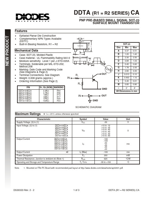
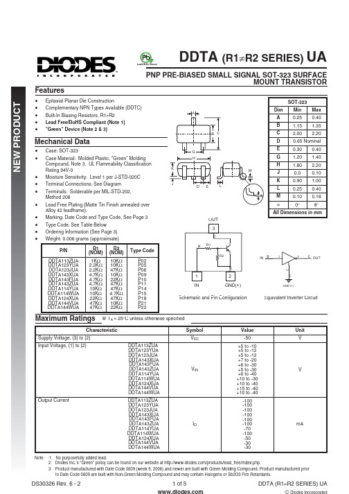
DDTC (R1≠R2 SERIES) UANPN PRE-BIASED SMALL SIGNAL SURFACE MOUNT TRANSISTORFeatures• Ordering Information: See Page 4 • Weight: 0.006 grams (approximate)P/N R1 (NOM) R2 (NOM) Type CodeDDTC113ZUA DDTC123YUA DDTC123JUA DDTC143XUA DDTC143FUA DDTC143ZUA DDTC114YUA DDTC114WUA DDTC124XUA DDTC144VUA DDTC144WUA 1K Ω2.2K Ω2.2K Ω 4.7K Ω4.7K Ω 4.7K Ω 10K Ω10K Ω22K Ω47K Ω47K Ω10K Ω 10K Ω 47K Ω 10K Ω 22K Ω 47K Ω 47K Ω 4.7K Ω 47K Ω 10K Ω 22K Ω N02 N05 N06 N09 N10 N11 N14 N15 N18 N21 N22SOT-323Dim Min Max A 0.25 0.40 B 1.15 1.35 C 2.00 2.20 D0.65 NominalE 0.30 0.40 G1.20 1.40 H 1.802.20 J 0.0 0.10 K 0.90 1.00 L 0.25 0.40 M0.100.18α0° 8° All Dimensions in mmMaximum Ratings @T A = 25°C unless otherwise specifiedCharacteristicSymbol Value Unit Supply Voltage, (3) to (2)V CC50 VInput Voltage, (1) to (2) DDTC113ZUA DDTC123YUA DDTC123JUA DDTC143XUA DDTC143FUA DDTC143ZUA DDTC114YUA DDTC114WUA DDTC124XUA DDTC144VUA DDTC144WUA V IN -5 to +10 -5 to +12 -5 to +12 -7 to +20 -6 to +30 -5 to +30 -6 to +40 -10 to +30 -10 to +40 -15 to +40 -10 to +40 VOutput Current DDTC113ZUA DDTC123YUA DDTC123JUA DDTC143XUA DDTC143FUA DDTC143ZUA DDTC114YUA DDTC114WUA DDTC124XUA DDTC144VUA DDTC144WUA I O 100 100 100 100 100 100 70 100 50 30 30 mAOutput Current AllI C (Max) 100mANotes: 1. No purposefully added lead. 2. Diodes Inc.'s "Green" policy can be found on our website at /products/lead_free/index.php. 3. Product manufactured with Date Code 0627 (week 27, 2006) and newer are built with Green Molding Compound. Product manufactured prior to Date Code 0627 are built with Non-Green Molding Compound and may contain Halogens or Sb2O3 Fire Retardants.R1OUT B CE R2321IN GND(0)132GND (0)C BIN OUTESchematic and Pin Configuration Equivalent Inverter CircuitMaximum Ratings (continued)@T A = 25°C unless otherwise specifiedCharacteristic Symbol Value Unit Output Current All I C (Max) 100 mA Power Dissipation P d200 mW Thermal Resistance, Junction to Ambient Air (Note 4) RθJA625 °C/W Operating and Storage Temperature Range T j, T STG-55 to +150 °CNotes: 4. Mounted on FR4 PC Board with recommended pad layout at /datasheets/ap02001.pdf.Electrical Characteristics@T A = 25°C unless otherwise specifiedCharacteristic Symbol Min Typ Max Unit Test ConditionInput Voltage DDTC113ZUADDTC123YUADDTC123JUADDTC143XUADDTC143FUADDTC143ZUADDTC114YUADDTC114WUADDTC124XUADDTC144VUADDTC144WUAV l(off)0.30.30.50.30.30.50.30.80.41.00.8⎯⎯V CC = 5V, I O = 100μAInput Voltage DDTC113ZUADDTC123YUADDTC123JUADDTC143XUADDTC143FUADDTC143ZUADDTC114YUADDTC114WUADDTC124XUADDTC144VUADDTC144WUAV l(on)⎯⎯3.03.01.12.51.31.31.43.02.55.04.0V V O = 0.3V, I O = 20mAV O = 0.3V, I O = 20mAV O = 0.3V, I O = 5mAV O = 0.3V, I O = 20mAV O = 0.3V, I O = 3mAV O = 0.3V, I O = 5mAV O = 0.3V, I O = 1mAV O = 0.3V, I O = 2mAV O = 0.3V, I O = 2mAV O = 0.3V, I O = 2mAV O = 0.3V, I O = 2mAOutput Voltage V O(on)⎯0.1 0.3 V I O/I l = 5mA/0.25mA DDTC123JUA I O/I l = 5mA/0.25mA DDTC143ZUA I O/I l = 5mA/0.25mA DDTC114YUA I O/I l = 10mA/0.5mA All OthersInput Current DDTC113ZUADDTC123YUADDTC123JUADDTC143XUADDTC143FUADDTC143ZUADDTC114YUADDTC114WUADDTC124XUADDTC144VUADDTC144WUAI l⎯⎯7.23.83.61.81.81.80.880.880.360.160.16mA V I = 5VOutput Current I O(off)⎯⎯0.5 μA V CC = 50V, V I = 0VDC Current Gain DDTC113ZUADDTC123YUADDTC123JUADDTC143XUADDTC143FUADDTC143ZUADDTC114YUADDTC114WUADDTC124XUADDTC144VUADDTC144WUAG l3333803068806824683356⎯⎯⎯V O = 5V, I O = 5mAV O = 5V, I O = 10mAV O = 5V, I O = 10mAV O = 5V, I O = 10mAV O = 5V, I O = 10mAV O = 5V, I O = 10mAV O = 5V, I O = 5mAV O = 5V, I O = 10mAV O = 5V, I O = 5mAV O = 5V, I O = 5mAV O = 5V, I O = 5mAInput Resistor Tolerance ΔR1-30 ⎯+30 % ⎯Resistance Ratio Tolerance ΔR2/R1-20 ⎯+20 % ⎯Gain-Bandwidth Product* f T⎯250 ⎯MHz V CE = 10V, I E = 5mA,f = 100MHz* Transistor - For Reference OnlyTypical Curves – DDTC123JUA-5005010025020015050100T , AMBIENT TEMPERATURE (C)Fig. 1 Derating CurveA °150P , P O W E R D I S S I P A T I O N (m W )D 0.0010.010.111020304050V , C O L L E C T O R E M I T T E R V O L T A G E (V )C E (S A T )I , COLLECTOR CURRENT (mA)Fig. 2 V vs. IC CE(SAT) C101,000100110h , D 100C C U R R E N T G A I NF E I , COLLECTOR CURRENT (mA)Fig. 3 DC Current GainC012342030C , C A P A C IT A N C E (p F )O B V , REVERSE BIAS VOLTAGE (V)Fig. 4 Output CapacitanceR 10515250.0010.01110100012348910I , C O L L E C T O R C U R R E N T (m A )C V , INPUT VOLTAGE (V)Fig. 5 Collector Current vs. Input Voltagein 5670.10.111010203040I , COLLECTOR CURRENT (mA)Fig. 6 Input Voltage vs. Collector CurrentC 50V , I N P U T V O L T A G E (V )i nOrdering Information (Note 3 & 5)Device Packaging Shipping DDTC113ZUA-7-F SOT-323 3000/Tape & ReelDDTC123YUA-7-F SOT-323 3000/Tape & ReelDDTC123JUA-7-F SOT-323 3000/Tape & ReelDDTC143XUA-7-F SOT-323 3000/Tape & ReelDDTC143FUA-7-F SOT-323 3000/Tape & ReelDDTC143ZUA-7-F SOT-323 3000/Tape & ReelDDTC114YUA-7-F SOT-323 3000/Tape & ReelDDTC114WUA-7-F SOT-323 3000/Tape & ReelDDTC124XUA-7-F SOT-323 3000/Tape & ReelDDTC144VUA-7-F SOT-323 3000/Tape & ReelDDTC144WUA-7-F SOT-323 3000/Tape & Reel Notes: 5. For packaging details, go to our website at /datasheets/ap02007.pdf.Marking InformationDate Code Key NXXYMNXX = Product Type Marking CodeSee Page 1 DiagramsYM = Date Code MarkingY = Year ex: T = 2006M = Month ex: 9 = SeptemberYear20022003200420052006200720082009201020112012 Code N P R S T U V W X Y ZMonth Jan Feb Mar Apr May Jun Jul Aug Sep Oct Nov Dec Code 1 2 3 4 5 6 7 8 9 O N DIMPORTANT NOTICEDiodes Incorporated and its subsidiaries reserve the right to make modifications, enhancements, improvements, corrections or other changes without further notice to any product herein. Diodes Incorporated does not assume any liability arising out of the application or use of any product described herein; neither does it convey any license under its patent rights, nor the rights of others. The user of products in such applications shall assume all risks of such use and will agree to hold Diodes Incorporated and all the companies whose products are represented on our website, harmless against all damages.LIFE SUPPORTDiodes Incorporated products are not authorized for use as critical components in life support devices or systems without the expressed written approval of the President of Diodes Incorporated.分销商库存信息:DIODESDDTC124XUA-7-F DDTC143XUA-7-F DDTC114WUA-7-F DDTC114YUA-7-F DDTC143FUA-7-F DDTC143ZUA-7-F DDTC144VUA-7-F DDTC144WUA-7-F DDTC144WUA-7 DDTC144VUA-7DDTC143ZUA-7DDTC123JUA-7 DDTC123JUA-7-F DDTC114WUA-7DDTC113ZUA-7 DDTC113ZUA-7-F DDTC114YUA-7DDTC124XUA-7 DDTC123YUA-7-F DDTC143FUA-7DDTC123YUA-7 DDTC143XUA-7。
1439-3;1439-4;中文规格书,Datasheet资料

PLATING Gold/Gold Tin/Tin Tin/Gold
PLATING OPTIONS
CONTACT
BODY SPRING
Gold
Gold
Tin/Lead Tin/Lead
Tin/ Lead
Gold
RoHS Compliant
Non-Compliant
.015 (.38) - .021 (.53) PIN - PRESS FIT
contact maintains retention after multiple insertions • Ideal for mounting transistors, resistors, diodes, IC’s and similar miniature components • Custom micro jacks manufactured to your specifications • Other platings available upon request
1641A 1641B 1641C .122 (3.1)
NON-RoHS
Mtg.
GOLD/GOLD TIN/TIN TIN/GOLD Hole
CAT. NO. CAT. NO. CAT. NO. Dia.
1697 1698 1699 .063 (1.60)
.025 (.64) - .037 (.94) PIN - SOLDER MOUNT
6-FINGER CLOSED ENTRY CONTACT
GOLD/GOLD TIN/TIN TIN/GOLD Hole
CAT. NO. CAT. NO. CAT. NO. Dia.
1603 1606 1607 .052 (1.32)
DTA143ZUBTL;中文规格书,Datasheet资料
Typ. -0.1 4.7 10 250
Max. -0.5 -0.3 -1.8 -0.5 6.11 12 -
Unit V V mA mA kW MHz
*1 Characteristics of built-in transistor *2 Each terminal mounted on a reference footprint
DIM A A1 A2 b c D E e HE L Lp x DIM e1 b2 l1
Dimension in mm/inches
© 2012 ROHM Co., Ltd. All rights reserved.
6/10
/
e1
2012.04 - Rev.A
VCC = -5V, IO = -100μA VO = -0.3V, IO = -5mA IO / II = -5mA / -0.25mA VI = -5V VCC = -50V, VI = 0V VO = -5V, IO = -10mA VCE = -10V, IE = 5mA, f = 100MHz
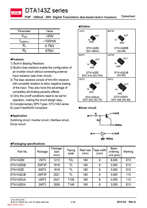
VCC IC(MAX.) R1 R2
lFeatures
-50V -100mA 4.7kW 47kW
EMT3
DTA143ZM (SC-105AA)
UMT3F OUT IN GND
DTA143ZEB (SC-89)
OUT IN GND
1) Built-In Biasing Resistors 2) Built-in bias resistors enable the configuration of an inverter circuit without connecting external input resistors (see inner circuit). 3) The bias resistors consist of thin-film resistors with complete isolation to allow negative biasing of the input. They also have the advantage of completely eliminating parasitic effects. 4) Only the on/off conditions need to be set for operation, making the circuit design easy. 5) Complementary NPN Types :DTC143Z series 6) Lead Free/RoHS Compliant. lApplication Switching circuit, Inverter circuit, Interface circuit, Driver circuit
DTC143ZUBTL;中文规格书,Datasheet资料
DTC143ZE SOT-416 (SC-75A)
UMT3 OUT IN GND SMT3
DTC143ZUB (SC-85)
OUT IN GND
DTC143ZUA SOT-323 (SC-70)
DTC143ZKA SOT-346 (SC-59)
lInner circuit
lPackaging specifications Part No. DTC143ZM DTC143ZEB DTC143ZE DTC143ZUB DTC143ZUA DTC143ZKA Package VMT3 EMT3F EMT3 UMT3F UMT3 SMT3 Package size (mm) 1212 1616 1616 2021 2021 2928 Taping code T2L TL TL TL T106 T146 Basic Reel size Tape width ordering (mm) (mm) unit (pcs) 180 180 180 180 180 180 8 8 8 8 8 8 8,000 3,000 3,000 3,000 3,000 3,000 Marking E23 E23 E23 123 123 E23
Data Sheet
EMT3F
D
A
x
S A
b e
HE
E
c
e
A2
A
A1
S
l1
b2
Patterm of terminal position areas
MILIMETERS MIN MAX 0.65 0.85 0.00 0.10 0.60 0.80 0.21 0.36 0.08 0.18 1.50 1.70 0.76 0.96 0.50 1.50 1.70 0.37 0.35 0.55 0.10 MILIMETERS MIN MAX 1.05 0.46 0.65 INCHES MIN 0 0.024 0.008 0.003 0.059 0.03 0.02 0.059 0.015 0.014 INCHES MIN MAX 0.041 0.018 0.026 0.022 0.004 0.067 MAX 0.004 0.031 0.014 0.007 0.067 0.038
DDTA143ECA中文资料
2005 S
Jan
Feb March Apr
May Jun
1
2
3
4
5
6
2006 T
2007 U
Jul Aug Sep
7
8
9
2008 V
2009 W
Oct
Nov Dec
O
N
D
DS30333 Rev. 2 - 2
2 of 3
DDTA (R1 = R2 SERIES) CA
NEW PRODUCT
Pd, POWER DISSIPATION (MILLIWATTS)
Output Current
All
Power Dissipation
Thermal Resistance, Junction to Ambient Air (Note 1)
Operating and Storage and Temperature Range
Symbol VCC
VIN
IO
IC (Max) Pd RqJA
J 0.013
K 0.903 1.10
L
0.45 0.61
M
0.85 0.80
a
0°
8°
All Dimensions in mm
SCHEMATIC DIAGRAM
Maximum Ratings @ TA = 25°C unless otherwise specified
Characteristic
hFE, DC CURRENT GAIN (NORMALIZED)
TYPICAL CURVES - DDTA143ECA
250
200
150
100
Z23S2445M01中文资料(AEROVOX)中文数据手册「EasyDatasheet - 矽搜」
•单和双额定值 - 双额定值
在SuperMet仅
所有SuperMet和ZEMAX电容TM集成•
60000小时使用寿命.
UL认证压敏灭弧删除•
电容稳定性±整个人生3%
电容器从电路在生命尽头.
•自清除金属化聚丙烯薄膜.
• 专利压力灭弧符合UL810
每个电容器填充有环氧化Soybeanoil
要求.
电介液.大豆油已被证明可靠性
所有AEROMET II电容都可以用时间和成本节约
EIA RS-186-3E状态测试要求.
AeroMount系统.触点厂家触点厂家对于需要reycled了解详细信息.
认证证书
EIA RS-186-2E湿度测试要求(TropiCAL条件).
• UL文件号E51176
• CSA文件号058450
• VDE认证可用
电气特性
• 温度范围:-40〜+ 70℃.源自• 电容范围3至80μF.
• 电容公差±10%.
• 电压范围240至480 VAC,60赫兹.
• 损耗因数0.1%以下
@ 60赫兹和25℃.
• 绝缘电阻千M
●μF.
•耐电压.
• 期限至足月1.75×WVAC
• 期限到案2×WVAC + 1KVAC
应用
• 窗式空调 • 单元式空调 • 电动汽车 • 风扇与鼓风机 • Pumps • 洗衣房设备 • 除湿机
注入
P = Supernol(M系列) S = SuperSoy(Z系列)
电压编码 电压第一个两位数
24 = 240 V交流 33 = 330 V交流 37 = 370 V交流 44 = 440 V交流 48 = 480 V交流 60 = 600 Vac
DDTA143ZUA-7-F中文资料
Symbol Min Typ Max
-0.3
-0.3
-0.5
Packaging SOT-323 SOT-323 SOT-323 SOT-323 SOT-323 SOT-323 SOT-323 SOT-323 SOT-323 SOT-323 SOT-323
Shipping 3000/Tape & Reel 3000/Tape & Reel 3000/Tape & Reel 3000/Tape & Reel 3000/Tape & Reel 3000/Tape & Reel 3000/Tape & Reel 3000/Tape & Reel 3000/Tape & Reel 3000/Tape & Reel 3000/Tape & Reel
+6 to -30
DDTA143ZUA
VIN
+5 to -30
V
DDTA114YUA
+6 to -40
DDTA114WUA
+10 to -30
DDTA124XUA
+10 to -40
DDTA144VUA
+15 to -40
DDTA144WUA
+10 to -40
Output Current
DDTA113ZUA
Mechanical Data
- 1、下载文档前请自行甄别文档内容的完整性,平台不提供额外的编辑、内容补充、找答案等附加服务。
- 2、"仅部分预览"的文档,不可在线预览部分如存在完整性等问题,可反馈申请退款(可完整预览的文档不适用该条件!)。
- 3、如文档侵犯您的权益,请联系客服反馈,我们会尽快为您处理(人工客服工作时间:9:00-18:30)。
Transistors DTA143ZKA / DTA143ZSA
Rev.A 1/3
-100mA / -50V Digital transistors (with built-in resistors)
DTA143ZM / DTA143ZE / DTA143ZUA / DTA143ZKA / DTA143ZSA
z Applications
Inverter, Interface, Driver
z Features
1) Built-in bias resistors enable the configuration of an inverter circuit without connecting external input resistors (see equivalent circuit).
2) The bias resistors consist of thin-film resistors with complete isolation to allow positive biasing of the input. They also have the advantage of almost completely eliminating parasitic effects.
3) Only the on/off conditions need to be set for operation, making the device design easy .
z Structure
PNP epitaxial planar silicon transistor (Resistor built-in type)
z External dimensions (Unit : mm)
Transistors DTA143ZKA / DTA143ZSA
Rev.A 2/3
z Packaging
TL UMT3
EMT3
SMT3
SPT
DTA143ZE DTA143ZM Part No.DTA143ZUA 3000T2L VMT3
8000
T1063000T1463000TP 5000DTA143ZKA DTA143ZSA
−−−−
−−−
−
−
−−−
−−−
−
−−−−
Package Packaging type Taping Taping Taping Taping Taping Code
Basic ordering
unit (pieces)
12
z Absolute maximum ratings (T a=25°C)
Limits
Parameter
Symbol V CC 150
200
300
−50−30 to +5−100−100
150−55 to +150DTA143ZE DTA143ZM DTA143ZUA DTA143ZKA DTA143ZSA
V V mA mW °C °C
V IN I O I C(Max.)P D Tj Tstg
Unit Supply voltage Input voltage Output current Power dissipation Junction temperature Storage temperature
z Electrical characteristics (T a=25°C)
Parameter
Symbol V I(off)V I(on)V O(on)I I I O(off)R 1G I R 2/R 1f T Min.−−1.3−−−3.29808−
−−−0.1−−4.7−10250
−0.5−−0.3−1.8−0.56.11−12−
V V CC =−5V, I O =−100µA V O =−0.3V, I O =−5mA I O /I I =−5mA/−0.25mA V I =−5V
V CC =−50V, V I =0V V O =−5V, I O =−10mA
V CE =−10V, I E =5mA, f =100MHz
∗
V mA µA k Ω−−−
−MHz
Typ.Max.Unit Conditions
Input voltage Output voltage Input current Output current Input resistance DC current gain Resistance ratio Transition frequency
∗ Characteristics of built-in transistor
Transistors DTA143ZKA / DTA143ZSA
Rev.A
z Electrical characteristic curves
I N P U T V O L T A G E : V I (o n ) (V )
OUTPUT CURRENT : I O (A)
−
−−−−−−−−−−Fig.1 Input voltage vs. output current
(ON characteristics)
−−1−−−−200−500−100−20−50−10−2−5INPUT VOLTAGE : V I(off) (V)
O U T P U T C U R R E N T : I o (A
)
Fig.2 Output current vs. input voltage
(OFF characteristics)
−D C C U R R E N T G A I N : G I
OUTPUT CURRENT : I O (A)
Fig.3 DC current gain vs. output
current
−−−−−−−−−−−OUTPUT CURRENT : I O (A)
O U T P U T V O L T A G E : V O (o n ) (V )
Fig.4 Output voltage vs. output
current
3/3
Appendix
About Export Control Order in Japan
Products described herein are the objects of controlled goods in Annex 1 (Item 16) of Export T rade Control
Order in Japan.
In case of export from Japan, please confirm if it applies to "objective" criteria or an "informed" (by MITI clause)
on the basis of "catch all controls for Non-Proliferation of Weapons of Mass Destruction.
Appendix1-Rev1.1。