Lattice XO中文使用教程
Lattice展示基于FPGA的安防和监控解决方案
距 离延 伸至 1 0 i n, 并 实现 高达 l 0 8 0 P的 分 辨 率 。
在 图像 信 号处 理 方 面 , L a t t i c e的 第 三 方 He l i o n公 司 推 出 了基 于 L a t t i c e F P G A的 9 0多 个 独 立 的 图 像 信 号 处 理方面 的 I P, 可 实现 高动 态 范 围成 像 ( HD R) 、 H. 2 6 4编 码器 、 自动对 焦 和 视频 分 析( 人 数 统计 、 入 侵 检 测 、目标 检 测 以及 摄 像 机 篡 改 检 测 ) 等, 客户可 根 据需求 定 制 I P,
( 本 刊供 稿)
S T公布 2 0 1 2年 i N E Mo 校 园设 计 大 赛 中国地 区获奖名 单
近1 3, 意 法半 导 体 宣 布 , 西 安 电 子科 技 大学 “ D r a g o n
器人以 S T M 3 2微 控 制 器 为 上 层 控 制 单 元 ,通 过 i N E M 0
板 载 加 速 度 计 、陀 螺 仪 和 地 磁 计 采 集 数 据 ,然 后 运 用 K a h n a n扩 展 滤 波 算 法 对 这 三 类 数 据 进 行 融 合 处 理 , 根 据 处 理 结 果 并 采 用 多 种 控 制 策 略 ,通 过 l 6路 舵 机 控 制 蛇 形 机器 人的每 个关节 , 使 机 器 人 在 复 杂 水 域 环 境 中 保 持 运 动稳定 性 , 从 而 实 现 了 对 蛇 形 机 器 人 的 闭 环 控 制 。 此
L a t t i c e展示 基于 F P G A的安 防和监控解 决方案
Quattro Micro中文操作手册
Quattro Micro 操作手册目录开启控制软件MassLynx二、以设定溶液开始质谱调谐,确定质谱仪的状态三、信号提取四、查看文件五、液相色谱操作程序六、测试送检样品之标准操作程序七、子离子扫描模式八、质量校正九、当长时间停电或移机必须关机时,关闭电源,和泄真空的程序一、开启控制软件MassLynx:1. 从桌面以鼠标左键双击MassLynx图示打开文件。
2. 开启后将自动开启的预设页面,如图示:3. 单击质谱调谐图示(MS Tune)以开启质谱控制页面4. 开启后质谱调谐页面如下:5. 该画面即为调谐和信号提取的主要画面。
二、以设定溶液(setup solution)开始质谱调谐,确定质谱仪的状态1. 在质谱调谐页面(MS Tune)选择扫描模式和扫描离子质量范围:选中全部四个扫描功能,选择全扫描(MS Scan),设定扫描质量(Mass)为175.1、609.3、1080.8、2034.6,扫描范围(Span)为10(或5)。
2. 以注射针筒抽取设定溶液(setup solution),以直接进样(infusion)的方式连接注射针和管路,让样品得以被注射针泵推送,直接进入质谱仪分析。
3. 在质谱调谐页面(MS Tune)以鼠标左键单击氮气(API GAS)和注射针的图示,接着单击开始操作键(Press for Operate),直到原本红灯的图标显示为绿灯(此时该图标所显示的文字为Press for Standby)。
单击注射针图示则注射针泵会开始运作而推送样品;单击氮气会开始供应三方面的氮气:雾化气体(nebulizing gas)、去溶剂气体(desolvation gas)、气帘气体(cone gas),可以确保样品的气化;而单击操作键之后会开始供应电压,使得样品带电形成离子并使离子通过质谱仪分析。
4. 在质量分析器页面(Analyzer)设定以下的数值,括号内的数值即为设定值:LM Resolution 1(15.0)、HM Resolution 1(15.0)、Ion Energy 1(0.0)、Entrance(50)、Collision(2)、Exit(50)、LM Resolution 2(15.0)、HM Resolution 2(15.0)、Ion Energy 2(3.0),此为配合质谱扫描的参数。
Lattice的ISPlever使用教程

Lattice的ISPlever使用教程Lattice的ISPlever使用教程ispLEVER使用教程目录第一节 ispLEVER 简介第二节 ispLEVER开发工具的原理图输入第三节设计的编译与仿真第四节硬件描述语言和原理图混合输入第五节 ispLEVER工具中VHDL和Verilog语言的设计方法第六节 ispVM System-在系统编程的软件平台第七节约束条件编辑器(Constraint Editor)的使用方法附录一 ispLEVER System上机实习题附录二 ispLEVER软件中文件名后缀及其含义第一节 ispLEVER 简介ispLEVER 是Lattice 公司最新推出的一套EDA软件。
设计输入可采用原理图、硬件描述语言、混合输入三种方式。
能对所设计的数字电子系统进行功能仿真和时序仿真。
编译器是此软件的核心,能进行逻辑优化,将逻辑映射到器件中去,自动完成布局与布线并生成编程所需要的熔丝图文件。
软件中的Constraints Editor工具允许经由一个图形用户接口选择I/O设置和引脚分配。
软件包含Synolicity公司的“Synplify”综合工具和Lattice 的ispVM器件编程工具。
ispLEVER软件提供给开发者一个简单而有力的工具,用于设计所有Lattice可编程逻辑产品。
软件支持所有Lattice公司的ispLSI 、MACH、ispGDX、ispGAL、GAL器件。
ispLEVER工具套件还支持Lattice新的ispXPGATM和ispXPLDTM产品系列,并集成了Lattice ORCA Foundry设计工具的特点和功能。
这使得ispLEVER的用户能够设计新的ispXPGA和ispXPLD产品系列,ORCA FPGA/FPSC系列和所有Lattice的业界领先的CPLD 产品而不必学习新的设计工具。
软件主要特征:1. 输入方式* 原理图输入* ABEL-HDL输入* VHDL输入* Verilog-HDL输入* 原理图和硬件描述语言混合输入2. 逻辑模拟* 功能模拟* 时序模拟3. 编译器* 结构综合、映射、自动布局和布线4. 支持的器件* 含有支持ispLSI器件的宏库及MACH器件的宏库、TTL库* 支持所有ispLSI、MACH、ispGDX、ispGAL、GAL、ORCA FPGA/FPSC、ispXPGA和ispXPLD 器件5. Constraints Editor工具* I/O参数设置和引脚分配6. ispVM工具* 对ISP器件进行编程软件支持的计算机平台:PC: Windows 98/NT/2000/XP第二节 ispLEVER开发工具的原理图输入I. 启动ispLEVER(按Start=>Programs=>Lattice Semiconductor=>ispLEVER Project Navigator)II. 创建一个新的设计项目A. 选择菜单File。
lattice 产品介绍

XP2 系列
LFXP2-17ELFXP2-17E-5FT256C
SC 系列
LFSCM3GA25EP1LFSCM3GA25EP1-5FN900C
SC 系统芯片在业 界领先的FPGA 体 系中集成了4到32 个3.8G Serdes , 可灵活配置成 GE/10GE.PCIE,OC12/48,Fiber channel,业界最 高速率2Gbps的 I/O接口,以及创 新的把结构化Asic 的MACO 块嵌入 了内部,因此和同 类产品相比,性能 更高,集成度更强
Low-Cost FPGAs
• Mainstream FPGA Features/Performance at Lower Cost – DDR/DDR2 – Full-Featured DSP – SERDES
System FPGAs
• Full System-level Solution for Communications Applications – World Class SERDES – Embedded Hard IP
Lattice 第一代通用 型FPGA,低成本, 外围配置芯片可采 用spi flash ,含有 dsp 模块,支持 DDR memory , 是实现简单算法设 计最好的选择
ECP2 系列
LFE2-6ELFE2-6E-5TN144C
ECP2 是业界最低成本 的90 nm的FPGA,以 前只有高端器件才有的 特点和性能,比如说pll 和dll的支持,高速的源 同步I/O,DDR,DDR2, 128Bit AES算法加密, 双端口dual-boot启动, SPI FLASH 加载,近 乎完美
XP 是单芯片,可以单 电源供电的FPGA,应用 于对安全性,单板面积 有要求的场合,而且 lattice 特有的TFR技 术,可以远程的不掉电 系统升级 XP2 也是单芯片的 FPGA ,但是加入了dsp 模块和供用户自己使用 的memory ,成本相比 xp也有降低,
Lattice XO2内部RAM使用手册
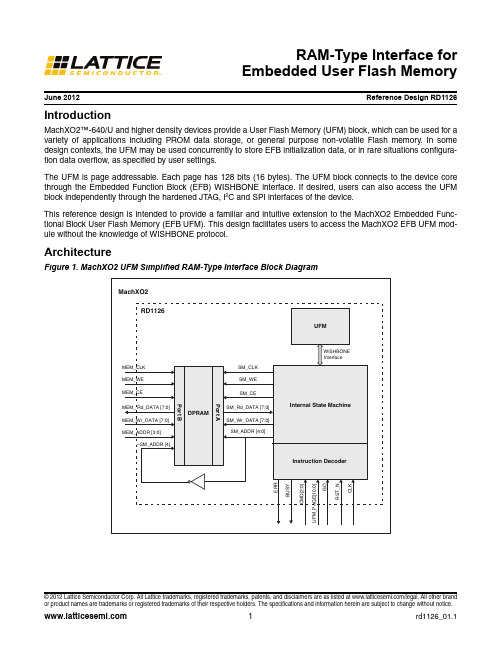
June 2012Reference Design RD1126© 2012 Lattice Semiconductor Corp. All Lattice trademarks, registered trademarks, patents, and disclaimers are as listed at /legal. All other brand or product names are trademarks or registered trademarks of their respective holders. The specifications and information herein are subject to change without notice.IntroductionMachXO2™-640/U and higher density devices provide a User Flash Memory (UFM) block, which can be used for a variety of applications including PROM data storage, or general purpose non-volatile Flash memory. In some design contexts, the UFM may be used concurrently to store EFB initialization data, or in rare situations configura-tion data overflow, as specified by user settings.The UFM is page addressable. Each page has 128 bits (16 bytes). The UFM block connects to the device core through the Embedded Function Block (EFB) WISHBONE interface. If desired, users can also access the UFM block independently through the hardened JTAG, I 2C and SPI interfaces of the device.This reference design is intended to provide a familiar and intuitive extension to the MachXO2 Embedded Func-tional Block User Flash Memory (EFB UFM). This design facilitates users to access the MachXO2 EFB UFM mod-ule without the knowledge of WISHBONE protocol.ArchitectureFigure 1. MachXO2 UFM Simplified RAM-Type Interface Block DiagramRAM-Type Interface forEmbedded User Flash MemoryPort DescriptionsTable 1. Port DescriptionsPort Direction Width (Bits)DescriptionCLK Input1Clock input1RST_N Input1Active low reset signalCommand InterfaceGO Input1High (‘1’) starts command process. GO is ignored if BUSY is asserted. CMD Input3Command operationUFM_P AGE Input11Target UFM PageBUSY Output1Status bit. Indicates operation in progress.ERR Output1Error bit. The last operation failed. Will be cleared on subsequent GO. Data InterfaceMEM_CLK Input1Clock for the DPRAM moduleMEM_WE Input1Write enable for the DPRAM moduleMEM_CE Input1Clock enable for the DPRAM moduleMEM_ADDR Input4DPRAM addressMEM_Wr_DA T A Input8DPRAM write dataMEM_Rd_DA T A Output8DPRAM read data1.Modify the design parameter READ_DELAY when CLK > 16.6 MHz. See discussion below.Functional DescriptionThis design facilitates user access to the MachXO2 EFB UFM module without the knowledge of WISHBONE proto-col. The user has to provide the necessary command sequence with UFM page address. A GO signal will trigger the interface to perform the necessary WISHBONE transactions to read or write the UFM.UFMThe User Flash Memory of the MachXO2 device features non-volatile storage in a single sector. Other features include:•Non-volatile storage up to 256Kbits•100K write cycles•Write access is performed page-wise; each page has 128 bits (16 bytes)•Auto-increment addressingTypical of Flash technology, the array must be cleared (erased) before data can be overwritten. The erased state of the UFM bits is ‘0’. The smallest erasable unit is the entire sector. Thus, any data which must be preserved (e.g. Config data overflow, or EBR init data) must be read out and stored in another available memory (e.g. EBR) prior to the Erase command. After the erase is complete, the data is written back to the UFM. The user is responsible for performing the storage operation. This requirement, along with limited erase cycles and long erase/program times, renders the UFM a poor solution for ‘scratch pad’ RAM (or similar) applications. MachXO2 Embedded Block RAM (EBR) is the recommended on-board memory type for high-churn, volatile data storage.In the design’s default configuration, the internal UFM read operation has been optimized for lower CLK rates. For CLK rates exceeding 16.6 MHz, this design must be configured to insert additional Retrieval Delay into the state machine which generates the UFM read command. A parameter, READ_DELAY, is provided for this purpose. The source file “UFM_WB_top.v” can be modified directly or the parameter passed in the module instantiation. The min-imum value for READ_DELAY can be calculated as follows:READ_DELAY(min) = 240/PERIOD - 4where PERIOD = CLK period in nsExample, for CLK = 47MHz, PERIOD = 21.28ns thus READ_DELAY >= 8 (7.28 rounded up)Refer to the “Reading Flash Pages” section of TN1204, MachXO2 Programming and Configuration Usage Guide for more information on the Read UFM command structure and timing requirements.DPRAMThe design incorporates a 32-byte (2 UFM page), byte addressable True Dual port RAM. The internal state machine accesses one port of the DPRAM. During the UFM write operation the state machine reads data from the DPRAM and writes it to the UFM. During UFM read operations the data read from the UFM is stored in the DPRAM.The second DPRAM port is accessed by the user to exchange data to or from the UFM. The DPRAM memory is divided into two pages of 16 bytes data each. The Most Significant Bit (MSB) of the DPRAM addresses are con-trolled by the internal state machine for page swapping. Thus, only one page (16 bytes) of the DPRAM is available through the user port at any given time. The available page is synchronized by the reference design and optimized for maximum throughput.During a UFM write operation, the DPRAM page swap happens once a GO is recognized. For higher throughput in back-to-back writes, this allows the user to immediately start loading the next page to be transferred to the UFM. During a read operation, the DPRAM page swap happens at the end of a read UFM operation and the user can start reading the DPRAM data once BUSY signal is low. In the case of back-to-back Read operations, the data remains available in the DPRAM until the subsequent Read is complete, allowing for higher throughput operation. CommandsTable 2. List of CommandsCommand Operation BUSY Signal Page Swap 000Read 1 page Clear when finished End of transaction001Read next page Clear when finished End of transaction010Write 1 page Clear upon UFM busy clear.Beginning of transaction011Write next page Clear upon UFM busy clear Beginning of transaction100Enable UFM access Clear upon UFM busy clear.N/A101Disable UFM access Clear when finished N/A110(undefined)––111Erase UFM Clear upon UFM busy clear N/ACommand Descriptions•Enable UFM access (100) – Required to enable UFM read/write access. Exercising this command will tempo-rarily disable certain features of the device, notably GSR, User SPI port and Power Controller. These features are restored when UFM access is disabled using Disable UFM access command (101). See TN1246, MachXO2 EFB User’s Guide, for more information on this behavior. BUSY is asserted until the devices internal Flash pumps are fully charged.•Write 1 page (010) – The 16 bytes of data from DPRAM is written into the UFM page specified by UFM_PAGE. The internal UFM page pointer is auto incremented at the completion of the command. Make sure that 16 bytes of data that has to be written to the UFM is loaded to the DPRAM prior to issuing a GO. BUSY will be asserted as soon as a GO is recognized and will be de-asserted when programming is complete.•Write next page (011) – The 16 bytes of data from DPRAM are written into the subsequent UFM page pointed by the internal UFM page pointer. The internal UFM page pointer is auto-incremented at the completion of thecommand. Make sure that 16 bytes of data that has to be written to the UFM is loaded to the DPRAM prior to issuing a GO. BUSY will be asserted as soon as a GO is recognized and will be de-asserted when programming is complete.•Read 1 page (000) – 16 bytes of data is read back from the UFM page specified by UFM_PAGE and stored in the DPRAM. The internal UFM page pointer is auto-incremented at the completion of the command. Following a Read command, the 16 bytes of UFM data can be read from the DPRAM after BUSY de-asserts.•Read next page (011) – The subsequent UFM page pointed by the internal UFM page pointer is read and stored into the DPRAM. The internal UFM page pointer is auto-incremented at the completion of the command. Follow-ing a Read command, the 16 bytes of UFM data can be read from the DPRAM after BUSY de-asserts.•Disable UFM access (101) – This command disables UFM interface for change access.•Erase UFM (111) – This command is issued to completely erase (set to ‘0’) the UFM. BUSY is asserted until era-sure is complete.Typical Command SequencesNotes:• A GO will be ignored when BUSY is asserted.•Any UFM read/write or erase command while UFM is disabled will assert the ERR signal.Write to UFMThe following sequence explains the necessary commands to be followed for a UFM write operation. The sequence assumes the target UFM row is in the erased state.1.Enable UFM access (100) – Check for BUSY signal to be low and issue enable UFM command on theCMD bus and issue a GO. BUSY signal is asserted once a GO is recognized.2.Write 1 page (010) – Load the DPRAM with one page (16 bytes) of data to be written to the UFM. Checkfor BUSY signal to be low, issue the Write 1 Page command on the CMD bus, UFM page address on the UFM_PAGE bus and issue a GO. The DPRAM page swap happens once a GO is recognized so that the user can load the next page to be written to the UFM into the DPRAM while the first page is being trans-ferred to the UFM.3.Write next page (011) – Wait for the previous page to be transferred to the UFM successfully and theBUSY signal goes low. Now issue a write next page command and issue GO. The internal UFM pagepointer is auto-incremented.4.Repeat steps 2 and 3 until all desired pages are written. Figure 2 illustrates steps 2 and 3.5.Disable UFM access (101) – Check for BUSY signal to be low and issue disable UFM command on theCMD bus and issue a GO. BUSY signal is asserted once a GO is recognized.Figure 2. Write to UFM Waveform DescriptionRead from UFMThe following sequence explains the necessary commands to be followed for a UFM read operation.1.Enable UFM access (100) – Check for the BUSY signal to be low and issue an enable UFM commandon the CMD bus and issue a GO. BUSY signal is asserted once a GO is recognized.2.Read 1 page (000) – Check for BUSY signal to be low, issue the Read 1 Page command on the CMDbus, UFM page address on the UFM_PAGE bus and issue a GO. Data read from UFM will be loaded in the DPRAM and user can access the data once BUSY signal goes low.3.Read next page (011) – Check for the BUSY signal to be low, issue the read next page command on theCMD bus and issue a GO. The internal UFM page pointer is auto. Data read from UFM will be loaded in the DPRAM and user can access the data once the BUSY signal goes low.4.Repeat steps 2 and 3 until all desired pages have been read. Figure 3 illustrates steps 2 and 3.5.Disable UFM access (101) – Check for the BUSY signal to be low and issue a disable UFM commandon the CMD bus and issue a GO. The BUSY signal is asserted once a GO is recognized.Figure 3. Read from UFM Waveform DescriptionRead Modify Write Back to UFMThe page read from UFM can be retained in the DPRAM and data modification may be performed directly on the DPRAM, followed by a Write 1 Page operation. The following sequence explains the necessary commands to be followed in order to modify the contents of UFM.Note: The modified data cannot be arbitrary. Only erased bits/bytes (=‘0’) of the UFM can be given new values. This sequence is provided to support applications where small amounts of data, or data unaligned to UFM page boundaries, is accumulated over time (e.g. a data logger application).1.Enable UFM access (100) – Check for BUSY signal to be low and issue an enable UFM command onthe CMD bus and issue a GO. BUSY signal is asserted once a GO is recognized.2.Read 1 page (000) – Check for BUSY signal to be low, issue the Read 1 Page command on the CMDbus, UFM page address on the UFM_PAGE bus and issue a GO. Data read from the UFM will be loaded in the DPRAM and is available to read or edit once the BUSY signal goes low.3.Modify DPRAM data as needed. The DPRAM data is byte addressable. The user may modify theintended byte(s) directly in the DPRAM. Alternatively, the data may be read from, and re-written to, theDPRAM.4.Write 1 page (010) – Once the data in the DPRAM has been modified or re-written, check for the BUSYsignal to be low, issue the Write 1 Page command on the CMD bus, set the UFM page address on theUFM_PAGE bus and issue a GO. Note that UFM page address must be specified for both read and write.5.Repeat steps 2 through 4 until all desired pages have been modified. Figure 4 illustrates steps 2through 4.6.Disable UFM access (101) – Check for the BUSY signal to be low and issue a disable UFM commandon the CMD bus and issue a GO. BUSY signal is asserted once a GO is recognized.Figure 4. Read-Modify and Write Back to UFM Waveform DescriptionHDL Simulation and VerificationEnable CommandFigure 5. Enable Command HDL Simulation WaveformWrite CommandFigure 6. Loading of DPRAM HDL Simulation WaveformFigure 7. Write to UFM Command Sequence HDL Simulation WaveformRead CommandFigure 8. Read from UFM Command Sequence HDL Simulation WaveformDisable CommandFigure 9. Disable Command HDL Simulation WaveformImplementationTable 3. Performance and Resource UtilizationTechnical Support AssistanceHotline:1-800-LATTICE (North America)+1-503-268-8001 (Outside North America)e-mail:techsupport@ Internet:Revision HistoryFamily Language Speed GradeUtilization fmax (MHZ)I/Os Architecture Resources MachXO21Verilog-3239 LUTs>50421- EFB1- EBR1. Performance and utilization characteristics are generated using LCMXO2-1200ZE-3TG100C with Lattice Diamond ® 1.4 design software.Date Version Change SummaryApril 201201.0Initial release.June 201201.1Updated design and document to include READ_DELAY parameteriza-tion.Appendix A. UFM Command SequencesThe following table explains the different UFM internal command structure involved for the various operations of this reference design.Table 4. MachXO2 Embedded Function Block CommandsOperation Command (Hex)Operand (Hex)Write Data Read Data Enable UFM Access (100)Enable UFM74 08 00 00——Status check F000 00 00— 1 byte status data Write One Page (010)Set Address B400 00 0040 00 aa aa1—Write UFM C900 00 0116 bytes data fromDPRAM—Status check F000 00 00— 1 byte status data Write Next Page (011)Write UFM C900 00 0116 bytes data fromDPRAM—Status check F000 00 00— 1 byte status data Read One Page (000)Set Address B400 00 0040 00 aa aa1—Read UFM CA10 00 01—16 bytes data from UFM Read Next Page (011)Read UFM CA10 00 01—16 bytes data from UFM Disable UFM Access (101)Disable UFM2600 00 00——Bypass FF FF FF FF——Erase UFM (111)Erase UFM0E08 00 00——Status check F000 00 00— 1 byte status data 1.The aa aa value is copied from the 11-bit UFM_PAGE module input.。
利用LatticeXP评估板使用LatticeMico8微控制器
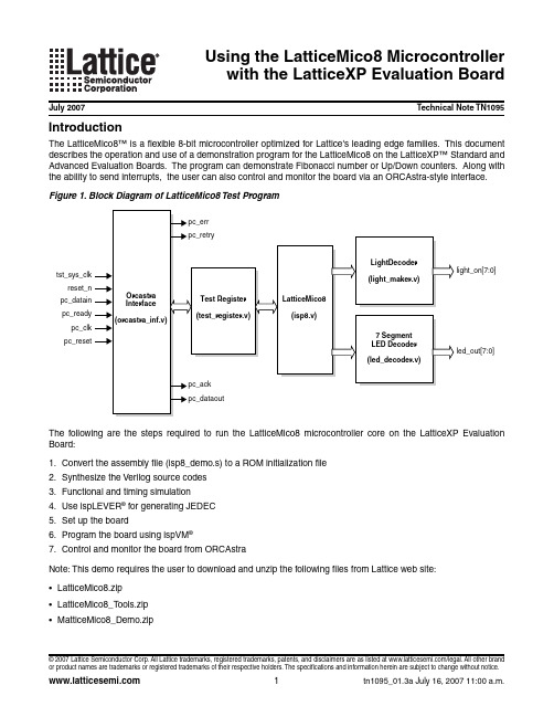
Usin g the LatticeMico8 Microcontrollerwith the LatticeXP Evaluation BoardJuly 2007Technical Note TN1095 IntroductionThe LatticeMico8™ is a flexible 8-bit microcontroller optimized for Lattice's leading edge families. This document describes the operation and use of a demonstration program for the LatticeMico8 on the LatticeXP™ Standard and Advanced Evaluation Boards. The program can demonstrate Fibonacci number or Up/Down counters. Along with the ability to send interrupts, the user can also control and monitor the board via an ORCAstra-style interface. Figure 1. Block Diagram of LatticeMico8 Test ProgramThe following are the steps required to run the LatticeMico8 microcontroller core on the LatticeXP Evaluation Board:1.Convert the assembly file (isp8_demo.s) to a ROM initialization file2.Synthesize the Verilog source codes3.Functional and timing simulatione ispLEVER® for generating JEDEC5.Set up the board6.Program the board using ispVM®7.Control and monitor the board from ORCAstraNote: This demo requires the user to download and unzip the following files from Lattice web site:•LatticeMico8.zip•LatticeMico8_T ools.zip•MatticeMico8_Demo.zip© 2007 Lattice Semiconductor Corp. All Lattice trademarks, registered trademarks, patents, and disclaimers are as listed at /legal. All other brandUsin g the LatticeMico8 Microcontroller Lattice Semiconductor with the LatticeXP Evaluation Board Step 1: Convertin g the Assembly File to a ROM Initialization fileFollow the instructions below to convert the assembly file.•Copy all the files in the directory LatticeMico8_Tools to directoryC:\<your_directory>\LatticeMico8_Demo\test•Open a DOS command window•Change the directory to C:\<your_directory>\LatticeMico8_Demo\test•In the command line, type: isp8asm_win -o prom_init.v -l -ve ..\asm\isp8_demo.s• A new ROM initialization file (prom_init.v) is generatedStep 2: Synthesizin g the Verilo g Source CodesAfter obtaining the prom_init.v file, the next step is to synthesize the Verilog source codes. The file name for the memory initialization file remains unchanged as prom_init.v since the file isp8.v will call the prom_init.v directly.•Open Synplify Synthesis•Add these files in the following order:~/LatticeMico8/ver2.4/models/xp/sim/dpram32x8.v~/LatticeMico8/ver2.4/models/xp/sim/prom.v~/LatticeMico8/ver2.4/models/xp/sim/spram32x8.v~/LatticeMico8/ver2.4/models/xp/sim/spram16x8.v~/LatticeMico8/ver2.4/models/xp/sim/spram16x9.v~/LatticeMico8/ver2.4/models/xp/syn/xp.v~/LatticeMico8/source/isp8.v~/LatticeMico8_Demo/source/test_register/test_register.v~/LatticeMico8_Demo/source/orcastra_inf/orcastra_inf.v~/LatticeMico8_Demo/source/led_decoder/led_decoder.v~/LatticeMico8_Demo/source/light_maker/light_maker.v~/LatticeMico8_Demo/source/top/isp8_top_system.v•Add the following source directory in the Include path:~/LatticeMico8_Demo/source/config3~/LatticeMico8_Demo/test•In the Implementation Options dialog box set the following options under Device tab:–Lattice T echnology = LATTICE XP–Part = LFXP10C–Speed = -5–Package = F256C (Standard Board) / F388C (Advanced Board)•Click RunNote: The above procedure is for synthesizing LatticeMico8 and the demo source codes. Users can synthesize LatticeMico8 (isp8.v) by itself from the LatticeMico8 directory by using the Tcl script located in the Synthesis direc-tory. Before using this Tcl script, please modify the PROJP A TH variable in the Tcl script to resemble the current project directory.Step 3: Functional and Timin g Simulation•Open ModelSim Simulator•From the menu bar, select File -> Chan g e Directory, and set the folder to ~/LatticeMico8_Demo/simula-tionUsin g the LatticeMico8 Microcontroller Lattice Semiconductor with the LatticeXP Evaluation Board •For functional simulation, from the menu bar, select Tools -> TCL -> Execute Macro, click on the Script direc-tory and select demo_func_sim.do•For timing simulation, the .vo and .sdf files must already be generated by ispLEVER Project Navigator and located at ~/LatticeMico8_Demo/par/top. From the menu bar, select Tools -> TCL -> Execute Macro, click on the Script directory and select demo_time_sim.do.Note: The demo_time_sim.do may need to be modified to match the .vo and .sdf file names.Step 4: Usin g ispLEVER for Generatin g JEDEC•Open ispLEVER Project Navigator•T o set the target device, in the Device Selector dialog box, select the following:–Family = LatticeXP–Device = LFXP10C or LFXP10E–Speed Grace = -5–Package T ype = FPBGA256 (Standard Board) / FPBGA388 (Advanced Board)–Operating Conditions = Commercial•From the Project Navigator, double click on Pre-Map Preference Editor to set the pin types and pin locations Table 1. Pin Assignment for LatticeXP Advanced & Standard BoardsSi g nal NamePin LocationI/O Type Standard Board Advanced Boardtst_sys_clk A7A10LVCMOS33 reset_n L12H3LVCMOS33 light_on_0D5H1LVCMOS33 light_on_1A3B16LVCMOS33 light_on_2B3B18LVCMOS33 light_on_3B2C18LVCMOS33 light_on_4A2C19LVCMOS33 light_on_5B1C20LVCMOS33 light_on_6F5W16LVCMOS33 light_on_7C5A16LVCMOS33 led_out_0J14D2LVCMOS33 led_out_1K16F3LVCMOS33 led_out_2K15F1LVCMOS33 led_out_3L14E2LVCMOS33 led_out_4L13E1LVCMOS33 led_out_5K13D1LVCMOS33 led_out_6N16F2LVCMOS33 pc_err H16B4LVCMOS33 pc_retry H12C4LVCMOS33 pc_ack F13A18LVCMOS33 pc_dataout G14C3LVCMOS33 pc_clk C15A3LVCMOS33 pc_ready F16B3LVCMOS33 pc_datain E14A2LVCMOS33 pc_reset C16A4LVCMOS33Usin g the LatticeMico 8 Microcontroller Lattice Semiconductorwith the LatticeXP Evaluation Board•Double click on Generate Timin g Simulation Files . This process will generate .vo and .sdf files that can be used for timing simulation•Double click on Generate Data File (JEDEC) to get the .jed file that will be used later with ispVM System to pro-gram the evaluation boardStep 5: Settin g up the BoardFor the LatticeXP Standard Evaluation Board:•Set the VCCIO pins of all banks of eight jumpers (JP1, JP2, JP12, JP11, JP13, JP14, JP10, and JP3) to 3.3V •The VCC core is set and defaulted to 1.2 V . Don’t change the setting of the VCC core, but keep it as its original setting at 1.2V•Use a 1.2 power supply and a 3.3V power supply that can provide adequate current to the board •T o interface with ORCAstra software, connect the parallel port pins as mentioned in T able 2Note: Unlike the LatticeXP Advanced Board, the Standard board does not have seven-segment display on the board. However, user can easily get a regular seven-segment display such as HDSP7501 and connect it with the pins mentioned in T able 1.For the LatticeXP Advanced Evaluation Board:•Set the V CCIO pins of all banks to 3.3 V by putting all eight jumpers J2-J4 to J1•Use a 5V power supply that can provide adequate current to the board•T o interface with ORCAstra software, connect the following parallel port pins to the board pins Table 2. ORCAstra Interface ConnectionsStep 6: Pro g rammin g the Board Usin g ispVM SystemThe following are the steps for programming the LatticeXP Evaluation Board:•Connect your PC to the target board using a Lattice ispDOWNLOAD ® Cable •Launch ispVM System software •Click File -> New •Click Edit -> Add DeviceParallel Port PinsSi g nal Name DirectionBoard/Pin LocationsStandard BoardAdvanced Board2(tied to 15) 6 PC_Data_InPC Out E14A27PC_Clk PC Out C15A38PC_Reset PC Out C16A49PC_Ready PC Out F16B310PC_Err PC In H16B411PC_Data_Out PC In G14C312PC_Retry PC In H12C413PC_Ack PC In F13A1815(tied to 2)———18-25GND———•Click Select and select LatticeXP-ES for Device Family, LFXP10E_ES for Device, 256_ball fpBGA (Standard board) / 388_ball fpBGA (Advanced board) for Package and then click OK•Click Browse under the Data File field and point to the JEDEC file previously created by the ispLEVER Project Navigator•Highlight Flash Pro g rammin g Mode from the Device Access Options field selection list•Highlight FLASH Erase, Pro g ram, Verify from the Operation field selection list•Click on the OK button•Click GO to program to LatticeXP deviceStep 7: Controllin g and Monitorin g the Evaluation Board from ORCAstraWith ORCAstra, users can control and monitor the evaluation board by writing and reading the registers in the test_register module inside the LatticeXP device.Download the latest ORCAstra software from the Lattice web site at the following address:/products/designsoftware/orcastra.cfm.After downloading ORCAstra, follow these steps to set it up with the board environment:•Launch ORCAstra•On menu bar, click on Device and select Zero No Device•In the same menu bar, click on Interface and select FPGA User Master via Parallel Port•From the menu bar, click on LPT:Port and select 2 0x378Figure 2. ORCAstra System Bus Control GUIThe demo files also come with an additional GUI specially created to support LatticeMico8. This GUI enables users to view the value of all the 32 registers together by clicking on the Read All Re g isters button.T o open the LatticeMico8 GUI from ORCAstra software (v112 or later):•From the menu bar, select Custom Pro g rammability --> Visual Window• A new smaller window will appear titled Custom Visual Interface•Select File --> Open from its menu bar•Browse and select isp 8_g ui.vis file located in LatticeMico8_Demo/gui directory A new window with LatticeMico8 logo will appear.Figure 3. LatticeMico8 GUI Derived From ORCAstraThe assembly file that was converted to a ROM initialization file in Step 1 contains a program that will determine the Fibonacci number and the Up/down counter based on the command that is given from ORCAstra.T able 3 lists the addresses and data that are accepted by the program based on the assembly code (isp8_demo.s).Table 3. List of Demo CommandsThe program will act accordingly based on the address and data written by the user from ORCAstra. For example,by typing Adrs = 00003 and Data = 11 in the ORCAstra GUI and pressing the WR button, the Fibonacci function will be run. The program will generate the first 12 Fibonacci numbers and store the results in Register 0 through Register 12. The value of one of these registers can be read by typing its address. For example, to read Register 0,type 00020 in the Adrs field and press the Rd button. The value will be shown in the Data field.Adrs (Address)Data Type of FunctionSpeed 0000311Fibonacci 1 (Very Slow)0000312Fibonacci 2 (Slow)0000313Fibonacci 3 (Medium)0000314Fibonacci 4 (Fast)0000321Up/Down Counter 1 (Very Slow)0000322Up/Down Counter 2 (Slow)0000323Up/Down Counter 3 (Medium)0000324Up/Down Counter 4 (Fast)0000201Sending Interrupt—Below is the list of registers and their corresponding addresses.Re g ister Name Re g0Re g1Re g2Re g3Re g4Re g5Re g6Re g7Address (hex)0002000021000220002300024000250002600027Re g ister Name Re g8Re g9Re g10Re g11Re g12Re g13Re g14Re g15Address (hex)00028000290002a0002b0002c0002d0002e0002fRe g ister Name Re g16Re g17Re g18Re g19Re g20Re g21Re g22Re g23Address (hex)0003000031000320003300034000350003600037Re g ister Name Re g24Re g25Re g26Re g27Re g28Re g29Re g30Re g31Address (hex)00038000390003a0003b0003c0003d0003e0003fTechnical Support AssistanceHotline:1-800-LA TTICE (North America)+1-503-268-8001 (Outside North America)e-mail:techsupport@Internet:Revision HistoryDate Version Chan g e SummaryJuly 200501.0Initial release.August 200601.2Updated to include LatticeXP Standard Evaluation Board.July 200701.3Updated block diagram (changed pc_data_in signal to read pc_datain).Updated file names in Step 2: Synthesizing theVerilog Source Codes.Clarified some of the menu selections in Step 3: Functional and TimingSimulation.Updated information on how to download ORCAstra software in Step 7:Controlling and Monitoring the Evaluation Board from ORCAstra.。
LatticeXO中文使用教程
LatticeXO中⽂使⽤教程Lattice MachXO TM设计指南v1.11.介绍 (4)1.1特征 (4)1.2产品系列和器件选择⼿册 (5)1.3性能分析 (6)2.体系结构 (7)2.1M ACH XO结构概述 (7)2.1.1PFU结构 (7)2.1.2Slice结构 (8)2.1.3布线资源 (9)2.2结构特征 (9)2.2.1时钟/控制信号⽹络 (9)2.2.2锁相环PLL (10)2.2.3⽚内时钟振荡器 (11)2.2.4嵌⼊块RAM (EBR) (11)2.2.5I/O特性 (11)2.2.6休眠模式 (13)2.2.7器件编程 (13)3.设计综合&实现 (14)3.1开发流程 (14)3.2设置约束项 (16)3.2.1设置I/O位置 &属性 (16)3.2.2设置时钟频率|周期 (16)3.2.3设置建⽴&保持时间 (17)3.2.4设置Tco时间 (19)3.2.5设置MutiCycles | MaxDelay | Tpd (20)3.2.6时序约束例外(BLOCK) (20)3.2.7信号分组 (20)4.器件应⽤要点 (21)4.1M ACH XO系列器件V CC,V CCAUX,V CCIO作⽤和连接 (21) 4.2M ACH XO系列器件各电源上电顺序及要求 (21)4.3M ACH XO热插拔应⽤注意事项 (21)4.4如何使⽤全局复位功能 (22)4.5如何使⽤全局输出三态功能 (22)4.6如何使⽤全局时钟 (23)4.7如何使⽤TFR功能(透明现场升级) (23)4.8如何使⽤M ACH XO的差分信号 (24)4.9如何接⼝5V输⼊信号 (25)4.10如何在同⼀B ANK使⽤不同I/O⼝电平标准 (25)4.11如何减⼩T CO时间 (26)4.12什么-M速度级别? (27)4.13如何获得时序分析结果? (27)4.14如何知道资源利⽤率 (28)4.15如何使⽤M ACH XO的块RAM(EBR) (28)4.16如何利⽤PFU⽣成移位寄存器和分布式RAM (29)4.17如何使⽤锁相环(PLL) (30)4.18下载接⼝(TAP)的连接建议 (30)4.19如何设置加密位和⽤户代码 (30)4.20如何使⽤P OWER C ACULTOR估计功耗 (31)4.21如何快速建⽴器件原理图库? (32)4.22如何选择综合⼯具? (32)4.23关于约束⽂件 (32)4.24如何使⽤M ODELSIM 进⾏仿真 (33)5.相关资料 (33)1.介绍MachXO器件是 Lattice 公司基于FLASH+SRAM技术CPLD器件。
使用lattice进行数据可视化--面板函数
使⽤lattice进⾏数据可视化--⾯板函数使⽤lattice进⾏⾼级绘图-- ⾯板函数每⼀个⾼⽔平的画图函数都采⽤了默认的函数来绘制⾯板图。
默认函数遵循命名规则panel.graph_function,其中graph_function指的是⾼⽔平的函数。
例如:xyplot(mpg~wt|displacement, data=mtcars)也可以写成:xyplot(mpg~wt|displacement, data=mtcars, panel=panel.xyplot)这是⼀个强⼤的功能,因为它可以让我们⽤⾃⼰设计的默认函数来代替默认的⾯板函数。
前⾯,我们画出了以汽车发动机排量为条件的汽车重量的油耗。
如果你想加上回归线、地毯图和⽹格线,需要做什么呢?我们可以通过创建⾃⼰的⾯板函数来实现它,代码如下:(1)⾃定义⾯板函数xyplotlibrary(lattice)displacement <- equal.count(mtcars$disp, number=3, overlap=0)#将四个独⽴的构件函数集成到⾃⼰的mypanel()函数中mypanel <- function(x, y) {panel.xyplot(x, y, pch=19)panel.rug(x, y)panel.grid(h=-1, v=-1) #panel.grid()函数添加⽔平和垂直的⽹格线(使⽤负数迫使其⽤轴标签排队)。
panel.lmline(x, y, col="red", lwd=1, lty=2)}xyplot(mpg~wt|displacement, data=mtcars,layout=c(3, 1),aspect=1.5,main = "Miles per Gallon vs. Weight by Engine Displacement",xlab = "Weight",ylab = "Miles per Gallon",panel = mypanel) #⾃定义⾯板函数,通过xyplot()函数中的panel=option选项使它⽣效结果分析:panel.xyplot()函数使⽤⼀个填充的圆(pch=19)产⽣散点图,也就是实⼼圆,panel.grid()函数添加⽔平和垂直的⽹格线(使⽤负数迫使其⽤轴标签排队),如图中的灰⾊⽹格线,panel.rug()函数把地毯图加到x轴和y轴的每个标签上,如图中的青绿⾊和蓝⾊短线条。
Lattice Reveal逻辑分析仪使用指南
Reveal 逻辑分析仪使用指南在Lattice的PLD开发平台的最新版本ISPLEVER7.0中新增加了一个成员,就是Reveal Logic Analyzer。
其最大的特点就是使用的步骤更为简单,更加的人性化。
目前Reveal逻辑分析仪支持的器件有LatticeECP/EC, LatticeXP, LatticeXP2,LatticeECP2, LatticeECP2S, LatticeECP2M, LatticeECP2MS, LatticeSC, and LatticeSCM。
使用Reveal逻辑分析仪之前先要插入一个逻辑分析仪的CORE到您的FPGA中,用于检测触发条件,存储数据等等。
下面这个流程做一个说明:1.首先就是建立一个工程,添加VHDL或者是VERILOG代码(对于RTL设计流程),或者EDIF网表(对于EDIF网表设计来说);2.点击ISPLEVER工具栏上的Reveal Inserter按钮,启动逻辑分析仪的插入。
图中鼠标所指位置。
3.新建或者是打开一个已经做好的reveal工程;在datasets下面可以建立多个CORE,每个CORE的内容可以不一样,最多16个CORE。
在SMAPLE CLOCK中加入您要作为采样时钟的时钟信号。
采样时钟也是可以不一样的,这就允许多时钟域的调试。
数据采样模式可以是单次,也可以是多次,取决于需要。
设置好测样的深度以及是否要包含触发信号。
加入需要作为触发的信号,或者是要观察的信号,设置好条件。
最多支持256个触发条件,操作类型支持==, !=, >=, >, <, =<, rising edge, falling edge, serial compare。
可以在左边的信号节点列表直接拖拽到触发单元列表中。
在触发单元中有一个radix,就是数的进制,其中有一个token类型,这是一个自定义的类型,可以自己编辑使用来观察状态机的。
LATTICE开发板原理图测试代码软件使用以及中文资料2
MachXO培训教程2005 年8 月英文网址:中文网址:或MachXO系列MachXO系列是新一代的跨越式可编程逻辑器件,支持传统上由高密度的CPLD或者低容量的FPGA所实现的应用,并且拥有更全面和高性能价格比的结构和工艺。
通过采用130nm的非易失性嵌入式Flash处理工艺,以及用于逻辑实现的业界标准,4-输入查找表(LUT)的方法,这些新的器件能让系统设计者在单位逻辑功能上降低50%的成本,而且在特性上有了很大的提升。
MachXO器件不仅能用来处理传统的CPLD应用,在该系列的所有成员中都增加了分布式存贮器、一种低待机功耗的睡眠模式以及通过莱迪思特有的TransFR技术来透明地更新逻辑配置的功能。
此外,在较大的系列成员中,增加了对嵌入式RAM(EBR)和锁相环(PLL)时钟电路以及PCI和LVDS I/O的支持,提供了通常仅在传统的FPGA结构中才有的功能。
与此同时,还保留了莱迪思前几代CPLD(如流行的MACH®器件)的瞬时上电、单片和高速的优点。
MachXO逻辑器件建立在低成本的130nm嵌入式Flash处理工艺上。
它能够在单芯片中瞬时工作,这种特性对于许多CPLD应用来说是十分重要的。
高达3.5ns的管脚至管脚的延时使得器件能够满足当代系统设计的高速要求。
MachXO有两种类型, “E”型和“C”型。
“E”型MachXO器件采用了1.2V逻辑核技术,适用于超低功耗的应用。
一个片上的电压调整器使得“C”型MachXO器件可以支持1.8V, 2.5V或3.3V的外部电压,从而支持传统的系统电源要求。
在每个器件的内核中是一个查找表阵列,可以用来实现逻辑和小型的分布式存储器。
这个阵列被灵活的I/O所包围,这些I/O能够实现多种流行的I/O标准,如LVCMOS。
在大一些的器件中,还支持PCI和LVDS。
器件的睡眠模式可减少100倍的待机功耗,支持那些要求低功耗的应用。
该器件还支持莱迪思特有的TransFR(透明的现场重新配置)技术,能够在器件使用SRAM配置存储器继续正常工作的情况下,对Flash配置存储器进行透明的编程。
- 1、下载文档前请自行甄别文档内容的完整性,平台不提供额外的编辑、内容补充、找答案等附加服务。
- 2、"仅部分预览"的文档,不可在线预览部分如存在完整性等问题,可反馈申请退款(可完整预览的文档不适用该条件!)。
- 3、如文档侵犯您的权益,请联系客服反馈,我们会尽快为您处理(人工客服工作时间:9:00-18:30)。
Lattice MachXO TM设计指南v1.11.介绍 (4)1.1特征 (4)1.2产品系列和器件选择手册 (5)1.3性能分析 (6)2.体系结构 (7)2.1M ACH XO结构概述 (7)2.1.1PFU结构 (7)2.1.2Slice结构 (8)2.1.3布线资源 (9)2.2结构特征 (9)2.2.1时钟/控制信号网络 (9)2.2.2锁相环PLL (10)2.2.3片内时钟振荡器 (11)2.2.4嵌入块RAM (EBR) (11)2.2.5I/O特性 (11)2.2.6休眠模式 (13)2.2.7器件编程 (13)3.设计综合&实现 (14)3.1开发流程 (14)3.2设置约束项 (16)3.2.1设置I/O位置 &属性 (16)3.2.2设置时钟频率|周期 (16)3.2.3设置建立&保持时间 (17)3.2.4设置Tco时间 (19)3.2.5设置MutiCycles | MaxDelay | Tpd (20)3.2.6时序约束例外(BLOCK) (20)3.2.7信号分组 (20)4.器件应用要点 (21)4.1M ACH XO系列器件V CC,V CCAUX,V CCIO作用和连接 (21)4.2M ACH XO系列器件各电源上电顺序及要求 (21)4.3M ACH XO热插拔应用注意事项 (21)4.4如何使用全局复位功能 (22)4.5如何使用全局输出三态功能 (22)4.6如何使用全局时钟 (23)4.7如何使用TFR功能(透明现场升级) (23)4.8如何使用M ACH XO的差分信号 (24)4.9如何接口5V输入信号 (25)4.10如何在同一B ANK使用不同I/O口电平标准 (25)4.11如何减小T CO时间 (26)4.12什么-M速度级别? (27)4.13如何获得时序分析结果? (27)4.14如何知道资源利用率 (28)4.15如何使用M ACH XO的块RAM(EBR) (28)4.16如何利用PFU生成移位寄存器和分布式RAM (29)4.17如何使用锁相环(PLL) (30)4.18下载接口(TAP)的连接建议 (30)4.19如何设置加密位和用户代码 (30)4.20如何使用P OWER C ACULTOR估计功耗 (31)4.21如何快速建立器件原理图库? (32)4.22如何选择综合工具? (32)4.23关于约束文件 (32)4.24如何使用M ODELSIM 进行仿真 (33)5.相关资料 (33)1.介绍MachXO器件是 Lattice 公司基于FLASH+SRAM技术CPLD器件。
FLASH存储用户配置程序,SRAM运行用户逻辑。
上电后,或者在JTAG命令控制下,MachXO自动执行FLASH到SRAM的传输。
MachXO集成了FPGA器件灵活性和传统CPLD器件的非易失特性于一身,为用户提供嵌入式RAM块(EBR),锁相环(PLL),差分I/O等特性。
并且支持不中断业务的现场升级能力(TFR技术)。
1.1特征·器件使用 .13μm SRAM + FLASH 工艺,有E版(1.2V)和C版(1.8/2.5/3.3V)两个版本 。
·非易失器件,瞬间上电( <1ms ),高安全性,单片解决方案。
·TFR技术保证现场升级过程I/O状态受控。
·高性能:系统性能超过250MHz,t PD=3.5ns。
·芯片由FLASH,可编程功能单元PFU,布线网络,嵌入式块RAM,锁相换PLL,I/O单元组成。
·FLASH存储用户程序,支持后台更新。
·PFU可实现逻辑,Ripple①,也可配置为分布式RAM,ROM。
·锁相环支持分频,倍频,移相。
周期抖动小于125ps。
·I/O可配为LVTTL,LVCMOSxx,LVDS,PCI。
·支持输出电流可调,输出边沿斜率可调,集电极开路,总线保持功能,内部上拉,下拉等。
·热插拔支持②。
·兼容IEEE 1149.1边界扫描标准(JTAG),IEEE 1532在系统编程标准。
·低的静态功耗2~10mA。
·休眠模式省电达100倍。
Note:① Ripple模式下,可高效的实现小的运算功能。
如2位计数,2位加减,2位比较等功能。
② 非True LVDS引脚,I DK < 1mA ( 0 < V IN <= V IHMAX ).True LVDS引脚, I DK < 1mA ( V IN <= V CCIO ).True LVDS引脚, I DK = 35mA ( V IN > V CCIO ).1.2产品系列和器件选择手册Table 1. MachXO 系列器件选择手册LCMXO256 LCMXO640 LCMXO1200 LCMXO2280 注查找表256 640 1200 2280 LUTs分布式RAM( Kbits) 2.0 6.0 6.25 7.5 Dist.嵌入式块RAM(Kbits) 0 0 1´ 9 3´ 9 EBR VCC电压 1.2/1.8/2.5/3.3V ①锁相环PLL 0 0 1 2最大I/O 78 159 211 271Package100-TQ (14X14) 78 74 73 73144-TQ (20X20) 113 113 113csBGA 100 (8X8) 78 74csBGA 132 (8X8) 101 101 101fpBGA 256 (17X17) 159 211 211fpBGA 324 (19X19) 271注:① XO器件有三组供电电压,分别为内核电源V CC,辅助电源V CCAUX ,I/O电源V CCIO .E版本器件V CC =1.2V, V CCAUX=3.3V, V CCIO =1.2/1.8/2.5/3.3V.C版本器件V CC =1.2/1.8/2.5/3.3V, V CCAUX=3.3V, V CCIO =1.2/1.8/2.5/3.3V.② MachXO 系列器件不同密度、相同封装的器件是引脚兼容的。
详情咨询技术支持。
③ MachXO 系列为dual mark 芯片,例如LCMXO640E-4F256C ,在此芯片上同时也被标注为-3I也就是说此芯片既可作为-4 commercial 芯片用,也可作-3 industrial 芯片用。
1.3性能分析下表列举了MachXO和Altera MAX II 以及 Lattice传统4k CPLD的指标对比。
Attribute MachXO MAX II 4000工艺130nm 180nm 180nm密度256~2280 LUTs 240~2210 LUTs 32~512 MicroCell Max I/O 78~271 80~272 32~208t PD 3.5ns (smallest device) 3.6ns(smallest device) 2.5~3.5nsI/O 标准LVTTLLVCMOSPCILVDSLVPECL LVTTLLVCMOSPCILVTTLLVCMOSPCI5V容忍-- -- Yes架构PFU阵列.每个PFU有 8个LUT4和8个寄存器组成.部分PFU可配置为分布式RAM. LAB阵列.每个LAB有10个LUT4和10个寄存器组成.所有LAB均不能配置为分布式RAM .GLB阵列.每个GLB有36输入,83乘积项,16个宏单元.没有分布式RAM.Block RAM 0~27.6Kbits None None PLLs 0~2 None None配置支持后台 FLASH编程.FLASH到SRAM的更新过程中I/O受控支持后台 FLASH编程.FLASH到SRAM的更新过程中I/O三态FLASH编程过程中I/O状态受控静态电流2~10mA(<100uA sleep) 2~10mA 2~13mA13~32uA(Z系列)操作电压 1.2V or 1.8/2.5/3.3V 1.8V or 2.5/3.3V 1.8V/ 2.5V/3.3VMachXO器件结合了FPGA和传统CPLD器件的优点,非常适合于逻辑容量介于高密度CPLD和低密度FPGA的之间交叉应用。
与竞争对手相比,先进的工艺和技术使得Lattice MachXO提供更低的成本和更好的特性。
2. 体系结构2.1MachXO 结构概述MachXO 系列器件由可编程功能单元(PFU),可编程I/O单元(sysIO),布线网络,嵌入式RAM块(EBR),模拟锁相环(PLL)等组成。
其中,XO256 不带锁相环,没有RAM块。
I/O分2个Bank.XO640 不带锁相环,没有RAM块。
I/O分4个Bank.XO1200一个锁相环,一个RAM块。
I/O分8个Bank.XO2280两个锁相环,三个RAM块。
I/O分8个Bank.Figure 1. XO2280结构框图2.1.1PFU结构MachXO的内核有PFU块和PFF块组成。
通过编程,PFU块可以实现逻辑,Ripple,分布式RAM和ROM等功能。
PFF除了不能实现分布式RAM外,等同于PFU。
以后将统称PFU。
每个PFU包含4 个slice。
PFU的输入和输出信号全部来自布线网络。
共有53个输入信号,25输出信号。
Figure2.PFU框图2.1.2Slice结构Slice有四种工作模式:逻辑, Ripple, 分布式RAM 或者分布式ROM。
逻辑模式下,LUT4 可实现任意4输入变量的逻辑式,LUT4的输出可以馈给对应的寄存器。
寄存器可工作在FF或者Latch模式下。
另外,还有附加的逻辑使得通过把LUT4组合,实现更宽输入的查找表(LUT5, LUT6, LUT7, LUT8)。
Ripple模式下,可高效的实现小的运算功能。
如2位计数,2位加减,2位比较等功能。
PFU(不含PFF)的LUT4可以配置为16位分布式RAM。
Figure3. Slice框图2.1.3布线资源布线资源有开关电路,缓冲器(buffer),金属线构成。
PFU之间的连接方式分为三种类型,X1类,X2类和X6类。
X1类连接相邻的PFU,提供了最小的延时;X2,X6类连接为跨越2个 PFU和6个PFU的PFU提供连接。
X2,X6类连接路径上插入了buffer,较X1 要慢些。
布局布线工具能够自动完成最佳路径的选择,布线资源的优化,无需人工干预。
用户也可以通过EPIC工具察看布线,并允许手动调整。
2.2结构特征2.2.1时钟/控制信号网络MachXO系列由4个初级全局时钟(primary)和4个次级全局时钟(secondary)。