TP5100中文datasheet
SPMC65P2204A_2202A_数据手册_V1.1

SPMC65P2204A/2202A
目录
頁次
1. 总述.............................................................................................................................................................................................................. 4 2. 特性.............................................................................................................................................................................................................. 4 3. 芯片结构概览 ............................................................................................................................................................................................... 5 4. 信号描述....................................................................................................................................................................................................... 6
MMBT5401-TP;中文规格书,Datasheet资料
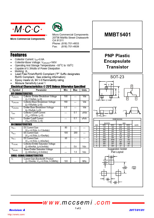
MMBT5401PNP Plastic Encapsulate TransistorFeatures• Collector Current:I CM =0.6A• Collector-Base Voltage:V (BR)CBO =160V• Operating And Storage Temperatures –55O C to 150O C • Capable of 0.3Watts of Power Dissipation • Marking:2LElectrical Characteristics @ 25OC Unless Otherwise SpecifiedSymbol ParameterMin Max Units OFF CHARACTERISTICSV (BR)CEO Coll e ctor -Emitter Breakdown Voltage (I C =1.0m Adc,I B =0)150--- Vdc V (BR)CBO Collector-Base Breakdown Voltage (I C =100uAdc,I E =0)160--- Vdc V (BR)EBO Emitter-Base Breakdown Voltage (I E =10uAdc,I C =0) 5.0--- VdcI CBO Collector Cutoff Current (V CB =120Vdc,I E =0)---0.1uAdcI EBOEmitter Cutoff Current (V EB =4.0Vdc,I C =0)---0.1uAdcON CHARACTERISTICSh FE-1DC Current Gain(V CE =5.0Vdc,I C =1.0mAdc)80------ h FE-2DC Current Gain(V CE =5.0Vdc,I C =10mAdc)100200--- h FE-3DC Current Gain(V CE =5.0Vdc,I C =50mAdc)50------V CE(sat)Collector-Emitter Saturation Voltage (I C =50mAdc,I B =5.0mAdc)---0.5Vdc V BE(sat)Base-Emitter Saturation Voltage (I C =50mAdc,I B =5.0mAdc)---1.0VdcSMALL-SIGNAL CHARACTERISTICSf TCurrent Gain-Bandwidth Product(I C =10mAdc,V CE =5.0Vdc, f=30MHz)100---MHzRevision: A 2011/01/01omp onents 20736Marilla Street Chatsworth! "# $ % ! "#Micro Commercial Componentswww.mccsemi .com1 of 2• Lead Free Finish/RoHS Compliant ("P" Suffix designates RoHS Compliant. See ordering information)• Epoxy meets UL 94 V-0 flammability rating • Moisure Sensitivity Level 1/Revision: A 2011/01/01Micro Commercial Componentswww.mccsemi .com2 of 23Ordering Information :***IMPORTANT NOTICE***Micro Commercial Components Corp. reserve s the right to make changes without further notice to any product herein to make corrections, modifications , enhancements , improvements , or other changes . Micro Commercial Components Corp . does not assume any liability arising out of the application or use of any product described herein; neither does it convey any license under its patent rights ,nor the rights of others . The user of products in such applications shall assume all risks of such use and will agree to hold Micro Commercial Components Corp . and all the companies whose products are represented on our website, harmless against all damages.***LIFE SUPPORT***MCC's products are not authorized for use as critical components in life support devices or systems without the express writtenapproval of Micro Commercial Components Corporation.***CUSTOMER AWARENESS***Counterfeiting of semiconductor parts is a growing problem in the industry. Micro Commercial Components (MCC) is taking strong measures to protect ourselves and our customers from the proliferation of counterfeit parts. MCC strongly encourages customers to purchase MCC parts either directly from MCC or from Authorized MCC Distributors who are listed by country on our web page cited below . Products customers buy either from MCC directly or from Authorized MCC Distributors are genuine parts, have full traceability, meet MCC's quality standards for handling and storage. MCC will not provide any warranty coverage or other assistance for parts bought from Unauthorized Sources. MCC is committed to combat this global problem and encourage our customers to do their part in stopping this practice by buying direct or from authorized distributors.DevicePackingPart Number-T PTape&Reel;3Kpcs/Reel/分销商库存信息: MICRO-COMMERICAL-CO MMBT5401-TP。
HL5100-G;HL-5200;HL-5100;HL-5200-G;HL-5300;中文规格书,Datasheet资料
HL-5300
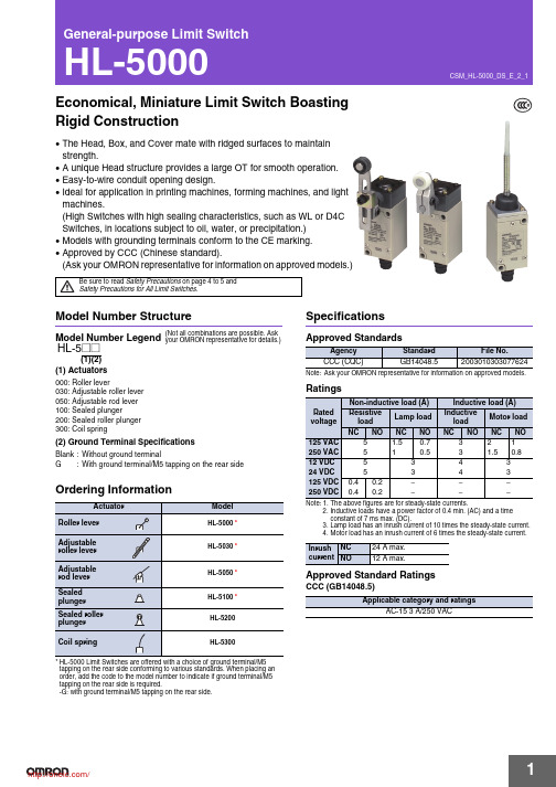
* HL-5000 Limit Switches are offered with a choice of ground terminal/M5 tapping on the rear side conforming to various standards. When placing an order, add the code to the model number to indicate if ground terminal/M5 tapping on the rear side is required. -G: with ground terminal/M5 tapping on the rear side.
(2) Ground Terminal Specifications
Blank : Without ground terminal G : With ground terminal/M5 tapping on the rear side
Ordering Information
Actuator Roller lever Adjustable roller lever Adjustable rod lever Sealed plunger Sealed roller plunger Coil spring Model
Dimensions and Operating Characteristics
Switches (Dimensions not shown are the same as roller lever models.)
Roller Lever HL-5000
58 ±0.8 53 ±0.8 39.5 ±0.8 40.3 ±0.8
TP05-1000-DBW中文资料
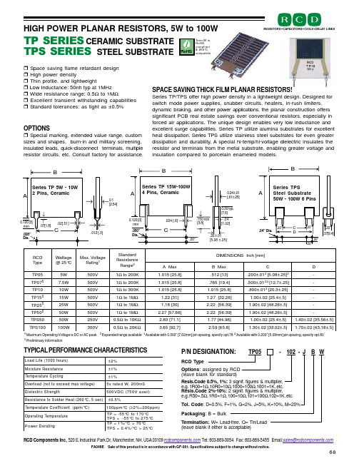
SPACE SAVING THICK FILM PLANAR RESISTORS!Series TP/TPS offer high power density in a lightweight design. Designed for switch mode power supplies, snubber circuits, heaters, in-rush limiters,dynamic braking, and other power applications, the planar construction offers significant PCB real estate savings over conventional resistors, especially in forced air applications. The unique design enables very low inductance and excellent surge capabilities. Series TP utilize alumina substrates for excellent heat dissipation. Series TPS utilize stainless steel substrates for even greater dissipation and durability. A special hi-temp/hi-voltage dielectric insulates the resistor and terminals from the metal substrate, enabling greater voltage and insulation compared to porcelain enameled models.OPTIONSSpecial marking, extended value range, custom sizes and shapes, burn-in and military screening,insulated leads, quick-disconnect terminals, multiple resistor circuits, etc. Consult factory for assistance.HIGH POWER PLANAR RESISTORS, 5W to 100WTP SERIES CERAMIC SUBSTRATE TPS SERIES STEEL SUBSTRATE1 Maximum Operating Voltage is DC or AC peak2 Expanded range available3 Available with 0.300” [7.62mm] pin spacing, specify opt.784 Available with 0.200” [5.08mm] pin spacing, specify opt.80 5Preliminary informationTYPICAL PERFORMANCE CHARACTERISTICSD C R e p y T e g a t t a W C °52@e g a t l o V .x a M g n i t a R 1d r a d n a t Se c n a t s i s e R e g n a R 2]m m [h c n I S N O I S N E M I D x a M A x a M B CD 50P T W 5V 0051ΩK 002o t ]8.52[510.1]31[215.10.±002.3]52.±80.5[3-70P T 5W 5.7V 0051ΩK 002o t ]8.52[510.1]4.91[567.10.±005.4,3]52.±7.21[-01P T W 01V 0051ΩK 003o t ]8.52[510.1]8.52[510.110.±008.3]52.±3.02[-51P T 5W 51V 0051ΩM 1o t Ω]13[22.1]62.23[72.1]5.±4.52[20.±00.1-52P T 5W 52V 0051ΩM 1o t Ω]03[81.1]93.65[22.2]5.±62.84[20.±09.1-05P T 5W 05V 0051ΩM 1o t Ω]66.75[72.2]93.65[22.2]5.±62.84[20.±09.1-05S P T W 05V 0525.0ΩK 01o t Ω]1.17[08.2]69.44[77.1]5.±4.52[20.±00.1]5.±65.53[20.±04.1001S P T W01V0035.0ΩK 02o t Ω]7.29[56.3]8.56[95.2]5.±20.33[20.±03.1]5.±81.34[20.±07.1)s r u o h 0001(e f i L d a o L %2±e c n a t s i s e R e r u t s i o M %1±e T p m e r u t a r e gn i l c y C %1±(d a o l r e v O )e g a t l o v x a m d e e c x e o t t o n S m 002,W d e t a r x 5ht g n e r t S c i r t c e l e i D )l i a v a V 057(C D V 005e c n a t s i s e R )c e s 5,C °062(t a e H r e d l o S o t %5.0±/m p p (t n e i c i f f e o C e r u t a r e p m e T )C °(C °m p p 001≥)m p p 002=%2er u t a r e p m e T g n i t a r e p O C °071o t C °55-=P T C °572o t C °55-=S P T r e w o P gn i t a r e D C °07>C °/%1=P T C°52>C °/%4.0=S P T FA048E Sale of this product is in accordance with GF-061. Specifications subject to change without notice.Space saving flame retardant design High power densityThin profile, and lightweightLow Inductance: 50nh typ at 1MHz Wide resistance range: 0.5Ω to 1M ΩExcellent transient withstanding capabilities Standard tolerances: as tight as ±0.5%.012 [.3]→0.1[2.54]←→ ← ||B|B|||B RCD Components Inc, 520 E.Industrial Park Dr, Manchester, NH, USA 03109 Tel: 603-669-0054 Fax: 603-669-5455 Email:sales@RESISTORS CAPACITOR S C OILS DELAY LINES68P/N DESIGNATION:Termination: W= Lead-free, Q= Tin/Lead (leave blank if either is acceptable)TP05 - 102 - J B WRCD TypePackaging : B = BulkTol. Code : D=0.5%, F=1%, G=2%, J=5%, K=10%, M=20%Options : assigned by RCD (leave blank for standard)Resis.Code 0.5%, 1%: 3 signif. figures & multiplier,e.g. 1R00=1Ω,10R0=10Ω,1000=100Ω,1001=1K, etc.Resis.Code 2%-10%: 2 signif. figures & multiplier,e.g. R50=.5Ω, 1R0=1Ω, 100=10Ω,101=100Ω,102=1K, etc.Term.W is RoHS compliant & 260°C compatible元器件交易网。
菲尼克斯5100说明书
菲尼克斯5100说明书菲尼克斯现货FL WLAN 5100 菲尼克斯现货FL WLAN 5100 WLAN接入点/端/中继器MIMO 3x3:2WLAN 02.11a、b、g、n2.4 GHz/5 GHz3根外置天线2x RJ 45尺寸(宽度 x 高度 x 深度)40 mm x 109 mm x 109 mm尺寸说明高度含天线插座,不含天线电缆FL WLAN以太网端口适配器是一款经济型工业WLAN 适配器,可将兼容以太网的设备连接到WLAN网络。
该以太网端口适配器外形紧凑,坚固耐用,内置无线模块和天线。
该设备防护等级达IP65,可直接现场安装,通过带M12连接器的以太网电缆连接到自动化设备。
优势:可直接在集成到应用以太网端口适配器的主要应用领域安装快捷轻松安装在现场以太网端口适配器是一种简易解决方案,可轻松将带以太网接口的工业自动化设备连接到WLAN网络。
该设备防护等级达IP65,可直接现场安装,通过带M12连接器的以太网电缆连接到自动化设备。
优势:内置天线的紧凑型IP65模块用于以太网和电力传输的M12接口轻松安装在现场自动组态,调试更简单安全通过Mode按钮轻松组态使用Mode按钮,无需组态即可轻松快速地构建安全的点到点网络和小型网络。
此外,也可通过网络浏览器轻松组态。
通过AT命令进行高级设置轻松组态和控制FL EPA 2在WLAN EPA模块运行过程中,可通过控制器发出的简单AT命令对其进行自动组态和控制。
这样就可以通过移动系统的控制器根据位置对漫游过程(即接入点之间的转换)进行控制。
FL EPA产品一览特性FL EPA 2FL EPA 2 RSMAWLAN标准IEEE 02.11a/b/gIEEE 02.11 a/b/g频段和道(*依不同国家而定)2.4 GHz,1-11道5 GHz:36-140道(端)5 GHz:36-4道(接入点)2.4 GHz,1-11道5 GHz:36-140道(端)5 GHz:36-4道(接入点)大数据速率(总值)54Mbps54 Mbps大数据流量(净值)< 20 Mbps< 20 Mbps运行模式端(单端网桥、多端网桥)(微型接入点)两个FL EPA模块之间的无线网桥端(单端网桥、多端网桥)(微型接入点)两个FL EPA模块之间的无线网桥大传输功率2.4 GHz:17 dBm(包括天线)5 GHz:15 dBm(包括天线)2.4 GHz:17 dBm(包括天线)5 GHz:15 dBm(包括天线)天线数1(内置)1(外置),RSMA接口安装后的防护等级IP65IP65环境温度(工作)-30°C … 60°C … 65°C电源9 … 30 V DC,大1.7 W9 …30 V DC,大1.7 W特殊性能双无线板:WLAN和蓝牙双无线板:WLAN和蓝牙功能强大的WLAN IEEE 02.11n模块,通范围更广采用新标准和MIMO技术,扩展通范围该设备有*的无线号,并采用符合IEEE 02.11n标准的MIMO(多点输入,多点输出)多天线技术,可在长距离范围内实现稳定、高速且可靠的无线通。
TP5410

RPROG (Ω) 10k 5k 1.2k 0.75k
IBAT 80mA 160mA 580mA 900 mA
个安全的电平,从而实现满电流充电。
0.68k
1000mA
当 BAT 引脚电压升至 2.9V 以上时,充
电器进入恒定电流模式,此时向电池提供恒
定的充电电流。当 BAT 引脚电压达到最终浮
充电压(4.2V)时,TP5410 进入恒定电压模
TP5410
工作原理
TP5410 是一款采用恒定电流/恒定电压 对单节锂离子电池充电和升压放电控制器。 它能够提供 1000mA 的充电电流(借助一个 热设计良好的 PCB 布局)。升压电路内置了 NMOS 功率管,外部仅需一个电感和肖特基二 极管及少量电容即可完成 5V 升压输出。
当 VOUT 端接入负载时,TP5410 可提供 一个 5V 的稳压源,驱动能力达 1A。
● 150 200
250
mA
PROG 引脚电压
RPROG=1.2K,充电模式
● 0.9
1.0
1.1
V
5
南京拓微集成电路有限公司
TP5410
VCHRG
CHRG 引脚输出低电压 ICHRG =5mA
0.3
VSTDBY
引脚输出低电平 ISTDBY =5mA
0.3
ΔVRECHRG 再充电电池门限电压
VFLOAT-VRECHRG
mA
升压无负载,VBAT=3.8V
●
-10 -100 μA
涓流充电电流
VBAT<VTRIKL,RPROG=1.2K
● 120 130
140
mA
涓流充电门限电压
RPROG=1.5K,VBAT 上升
N50P111;中文规格书,Datasheet资料

DatasheetEasyPoint TMN50P111Navigation Module1 General DescriptionEasyPoint™ N50P111 is a miniature joystick module concept based on contact-less, magnetic movement detection. The integrated two-dimensional linear encoder monitors the movement of the magnet incorporated in the knob and provides directly the x and ycoordinates via I²C output. An integrated mechanical push button built in the module provides a “select” function.Figure 1. N50P111-xxxxx-H2 Key FeaturesXY coordinates direct read with 8-bit resolution 2.7V to 3.6V operating voltage Down to 1.7V I/O voltageLateral magnet movement radius up to 2.0mm High-speed I²C interfaceConfigurable interrupt output for motion detection Push button feature3 ApplicationsThe EasyPoint™ N50P111 is ideal for small form-factor manual input devices in battery operated equipment, such as Mobile phones, MP3 players, PDAs, GPS receivers, Gaming consoles and Analog joystick replacement.4 BenefitsHigh reliability due to magnetic non-contact sensing Low power consumption Two operating modes-Idle mode-Low Power modeN50P111Push button GNDI²C AddressGND: 0x40VDDp: 0x41AS5013Two-dimensional magnetic encoderContents1 General Description (1)2 Key Features (1)3 Applications (1)4 Benefits (1)5 Pin Assignments (4)5.1 Pin Descriptions (4)6 Absolute Maximum Ratings (5)7 Electrical Characteristics (6)7.1 Operating Conditions (6)7.2 Digital IO Pads DC/AC Characteristics (6)7.3 Switch Characteristics (7)7.4 Mechanical Specifications (8)7.5 Recommended Reflow Temperature Profile (8)8 Using the N50P111 Module (9)8.1 Powering up the Module (9)8.2 Registers Initialization (9)8.3 C Source Code Example (10)8.3.1 Initialization (10)8.3.2 Offset Calibration (10)8.3.3 Dead Zone area (11)8.3.4 Interrupt Routine (11)9 XY Coordinates Interpretation (12)9.1 EasyPoint Operating Principle (12)9.1.1 Knob Displacement and Register Value Relation (13)9.2 Operation Principle (14)10 I²C interface (15)10.1 Interface Operation (15)10.2 I²C Electrical Specification (16)10.3 I²C Timing (17)10.4 I²C Modes (18)10.4.1 Automatic Increment of Address Pointer (18)10.4.2 Invalid Addresses (18)10.4.3 Reading (18)10.4.4 Writing (18)10.4.5 High Speed Mode (21)10.4.6 Automatic Increment of Address Pointer (22)10.4.7 Invalid Addresses (22)10.5 SDA, SCL Input Filters (22)11 I²C Registers (23)11.1 Control Register 1 (0Fh) (23)11.2 X Register (10h) (25)11.3 Y_res_int Register (11h) (25)11.4 Xp Register (12h) (25)11.5 Xn Register (13h) (25)11.6 Yp Register (14h) (26)11.7 Yn Register (15h) (26)11.8 M_ctrl Register (2Bh) (26)11.9 J_ctrl Register (2Ch) (27)11.10 T_ctrl Register (2Dh) (27)11.11 Control Register 2 (2Eh) (27)11.12 Registers Table (28)12 Package Drawings and Markings (30)Datasheet - P i n A s s i g n m e n t s5 Pin Assignments5.1 Pin DescriptionsTable 1. Pin DescriptionsConnector Pin #Pin Type Description 1Power VDDp: IO power supply for SCL, SDA, INTn, 1.7V ~ 3.6V2Power VDD: Core power supply, 2.7V ~ 3.6V3Power GND4Bi-directional SDA: I²C bus data, open drain5Input SCL: I²C bus clock6Input RESETn: Reset input, active LOW0: GND → Reset, all registers return to their reset value 1: VDDp → Normal operation mode7Open drain INTn: Interrupt output, open drain: Active: LOWInactive: Hi-Z8Output SWITCHn: Push button signal output: Not pushed: OpenPushed: GND9Input ADDR: I²C Address selection input:0: GND → 0x401: VDDp → 0x411234J1VDDVDDpSCLSDAGNDDatasheet - A b s o lu t e M a x im u m R a ti n g s6 Absolute Maximum RatingsStresses beyond those listed in Table 2 may cause permanent damage to the device. These are stress ratings only, and functional operation of the device at these or any other conditions beyond those indicated in Electrical Characteristics on page 6 is not implied. Exposure to absolute maximum rating conditions for extended periods may affect device reliability.Table 2. Absolute Maximum RatingsSymbol Parameter Min Max Units NotesV DD DC supply voltage-0.35VVDDp Peripheral supply voltage-0.35VDD + 0.3V SCL, SDA, RESETn, ADDRV IN Input pin voltage -0.3VDDp + 0.3VSCL, SDA, RESETn, ADDR - 3.6VI SCR Input current (latchup immunity)-100100mA Norm: JEDEC 78ESD Electrostatic discharge-±2kV All pins, Norm: MIL 883 E method 3015 T Strg Storage temperature-4085ºCHumidity non-condensing585%Degrees of protection IP5X Norm: IEC 605297 Electrical Characteristics7.1 Operating ConditionsT AMB = -20 to +70ºC, VDD = 3.3V 7.2 Digital IO Pads DC/AC CharacteristicsTable 3. Operating Conditions Symbol ParameterMin TypMax Units NotesVDDCore Supply voltage2.73.6VVDDp Peripheral Supply voltage 1.7VDD VInput: RESETnOpen drain outputs: SCL, SDA, INTn.External I²C pull up resistor to be connected to VDDp.IDD SMaximal average current consumption on VDD,Pulsed peaks = IDD fdepends on the sampling time ts[ms]3+3760/ts [ms]µAT AMB = -20 to +50 ºC10+3760/ts [ms]T AMB = 50 to +70 ºC IDD I Current consumption on core supply, Idle mode,no readout (ts = infinite)3µAT AMB = -20 to +50 ºC10T AMB = 50 to +70 ºC IDD f Current consumption on core supply,Full Power mode 10mA Continuous current pin VDD Maximum sampling ts = 450µs Tpua Power up time analog 1000µs Step on VDD to Data_Ready Tconv Conversion time 450µs Read X/Y coordinate I²C STOP condition to Data_Readyt P,W Nominal wakeup time 20320ms T AMBAmbient temperature range -20+70ºCResolution of XY displacement8Over 2*dx and 2*dy axisTable 4. Digital IO Pads DC/AC Characteristics Symbol ParameterMinMaxUnitsNotesInputs: SCL, SDAV IH High level input voltage 0.7 * VDDpV I²C V IL Low level input voltage 0.3 * VDDpV I²C I LEAK Input leakage current 1µA VDDp = 3.6V Inputs: ADDR, RESETn (JEDEC76)V IH High level input voltage 0.65 * VDDpV JEDEC V IL Low level input voltage 0.35 * VDDpV JEDEC I LEAK Input leakage current1µAVDDp = 3.6VOutputs: SDAV OHHigh level output voltageOpen drainLeakage current 1µA High level outputvoltage7.3 Switch CharacteristicsV OL1Low level output voltageVSS + 0.4V-6mA; VDDP > 2V;fast mode V OL3VDDP * 0.2V-6mA; VDDP ≤ 2V;fast mode V OL1VSS + 0.4V-3mA; VDDP > 2V;high speed V OL3VDDP * 0.2V -3mA; VDDP ≤ 2V;high speed C L Capacitive load 400pF standard mode ( 100 kHz )400pF fast mode ( 400 kHz )100pFhigh speed mode ( 3.4 MHz )Outputs: INTn (JEDEC76)V OH High level output voltage Open drain1µA Leakage current High level output voltageV OL Low level output voltageVSS + 0.2V -100µA VSS + 0.45-2mA C LCapacitive load30pFstandard mode ( 100 kHz )Table 5. Switch CharacteristicsParameterMinMax Units Notes Contact resistance of dome switch 750m ΩNorm: EIA-364-23Dielectric withstanding voltage100Vac Norm: EIA-364-20Insulation resistance 100m ΩNorm: EIA-364-21, 100VdcBouncing (On/Off)5msRate: 2 times/sec.Table 4. Digital IO Pads DC/AC Characteristics Symbol ParameterMinMax Units Notes7.4 Mechanical Specifications7.5 Recommended Reflow Temperature ProfileTable 6. Mechanical SpecificationsParameter Note Number of operating shaftsSingle shaft Shaft material LCP Housing material LCP & PA46Shell material Stainless Steel or Copper alloyTravel (XY operation)±2.00mm (±10%)Travel (Z push operation)0.22mm (±0.05mm)Directional operating force (XY direction)0.70N (±0.15N)Push operating force (Z direction)1.80N (±15%)Vibration10-500-10Hz 15 minutes, 12 cycles, 3 axes (total 36 cycles)Operating life – XY direction Each direction > 1 million cyclesOperating life – Push Z direction > 1 million cyclesShaft strength (XYZ direction)> 3.5 kgfFree fall Dispensing Glue40 drops(2X6 sides + 1X12 edges + 2X8 corners) @ 1.5m drop height to concrete surface, module is assembled to phone mechanics.Over forceDispensing Glue 1.5kgf > 100k cycles8 Using the N50P111 Module8.1 Powering up the ModuleThe N50P111 module has a Power ON Reset (POR) cell to monitor the VDD voltage at startup and reset all the internal registers. After the internal reset is completed, the POR cell is disabled in order to save current during normal operation.If VDD drops below 2.7V down to 0.2V, the POR cell will not be enabled back, and the registers will not be correctly reseted or can get random values.Note:It is highly recommended to control the external RESETn signal by applying a LOW pulse of >100ns once VDD has reached 2.7V and VDDp reached 1.7V.8.2 Registers InitializationAfter Power Up, the following sequence must be performed:1. VDD and VDDp Power up, and reached their nominal values (VDD>2.7V, VDDp>1.7V).2. Initialization:a. RESETn pulse LOW during >100ns, then RESETn HIGHb. Loop check register [0Fh] until the value F0h or F1h is present (reset finished, registers to default values)c. Write value 16h into register [2Dh]3. Perform an Offset Calibration (X and Y coordinate compensation for zero position)4. Configure the Dead Zone Area for Wake-up function (if needed)5. Configure the wanted Power Mode and INT function into register [0Fh] (Idle mode / Low Power Mode with Timebase configuration, INTfor Wake-up or Coordinates ready)6. X Y coordinates are ready to be read.8.3 C Source Code Example8.3.1 Initializationvoid EasyPoint_init (void){unsigned char Reset_status = 0;RESETn = 0;Delay_ms(1);// RESETn pulse after power upRESETn = 1; Delay_ms(1);while (Reset_status != 0xF0)// Check the reset has been done{Reset_status = I2C_Read8(0x40, 0x0F) & 0xFE;}I2C_Write8(0x40, 0x2E, 0x16); // Scaling factor for N50 (2.0mm knob travel) }8.3.2 Offset Calibrationvoid Offset_Calibrate (void){char i;int x_cal=0, y_cal=0;EA = 0;// Disable the MCU interruptsI2C_Write8(0x40, 0x0F, 0x00);// Low Power Mode 20msDelay_ms(1);I2C_Read8(0x40, 0x11); // Flush an unused Y_reg to reset the interruptfor (i=0; i<16; i++)// Read 16 times the coordinates and then average{while (INTn);// Wait until next interrupt (new coordinates)x_cal += (signed char) I2C_Read8(0x40, 0x10); // Read X positiony_cal += (signed char) I2C_Read8(0x40, 0x11); // Read Y position }// offset_X and offset_Y are global variables, used for each coordinate readout in the interrupt routineoffset_X = -(x_cal>>4); // Average X: divide by 16offset_Y = -(y_cal>>4); // Average Y: divide by 16EA = 1; // Enable the MCU interrupts}分销商库存信息: AMSN50P111。
TP5100中文数据手册

TP5100
南京拓品微电子有限公司
NanJing Top Power ASIC Corp.
数据手册 DATASHEET
TP5100
器芯片
U
2A开关降压 8.4V/4.2V锂电池充电
南京拓品微电子有限公司
TP5100
概述
TP5100是一款开关降压型双节8.4V/单节4.2V锂电池充电管理芯片。 其QFN16超小型封装 与简单的外围电路, 使得TP5100非常适用于便携式设备的大电流充电管理应用。 同时, TP5100 内置输入过流、欠压保护、芯片过温保护、短路保护、电池温度监控、电池反接保护。 TP5100具有5V-18V宽输入电压,对电池充电分为涓流预充、恒流、恒压三个阶段,涓流 预充电电流、 恒流充电电流都通过外部电阻调整, 最大充电电流达2A。 TP5100采用频率400kHz 的开关工作模式使它可以使用较小的外围器件,并在大电流充电中仍保持较小的发热量。 TP5100内置功率PMOSFET、防倒灌电路,所以无需防倒灌肖特基二极管等外围保护。
R R R R
PWR_ON-(引脚 6):电源切换控制引脚。 当芯片接电源时, PWR_ON- 被内部开关拉 到低电平,驱动 PMOS 导通,当芯片不接电 源时,PWR_ON-被内部开关拉到高电平为 BAT 端电池电压,驱动 PMOS 关断。此引 脚可以用于电源供电切换, 也可用作检测电 源上电建立是否正常。 GND(引脚 7) :电源地。 VS(引脚 8) :输出电流检测的正极输入端。 BAT(引脚 9) :电池电压检测端。将电池 的正端连接到此管脚。 VREG(引脚 10) :内部电源。VREG 是一个 内部电源, 它外接一个 0.1uF 旁路电容到地, 可以最大驱动 5mA。 TS(引脚 11) :电池温度检测输入端。将 TS 管脚接到电池的 NTC(负温度系数热敏 电阻)传感器的输出端。如果 TS 管脚的电 压小于 VREG 的 45%或者大于 VREG 电压 的 80%,意味着电池温度过低或过高,则充 电被暂停。如果 TS 直接接 GND,电池温度 检测功能取消,其他充电功能正常。
- 1、下载文档前请自行甄别文档内容的完整性,平台不提供额外的编辑、内容补充、找答案等附加服务。
- 2、"仅部分预览"的文档,不可在线预览部分如存在完整性等问题,可反馈申请退款(可完整预览的文档不适用该条件!)。
- 3、如文档侵犯您的权益,请联系客服反馈,我们会尽快为您处理(人工客服工作时间:9:00-18:30)。
STDBY (引脚 14) :绿灯电池充电完成指 示端。 当电池充电完成时 STDBY 被内部开
关拉到低电平,表示充电完成。除此之外,
STDBY 管脚将处于高阻态。 :红灯充电中状态指示 CHRG (引脚 15) 端。当充电器向电池充电时, CHRG 管脚
被内部开关拉到低电平,表示充电正在进 行;否则 CHRG 管脚处于高阻态。
RTRICK (引脚 12) : 涓流预充电流设置端。 将 RTRICK 引脚接地则预充电电流为 10% 设置恒流, 通过外接电阻可以设置预充电电 流。 如果 RTRICK 悬空则预充电电流等于恒 流电流。 CS(引脚 13) :锂离子状态片选输入端。CS 端高输入电平(VREG)将使 TP5100 处于 锂离子电池充电 8.4V 关断电压状态。CS 端 悬空使 TP5100 处于锂离子电池 4.2V 关断电 压状态。低输入电平使 TP5100 处于停机状 态。 CS 端可以被 TTL 或者 CMOS 电平驱动 控制。
t RECHARGE
R
V BAT 高至低
R R
mS mS
t TERM
R
I BAT 降至C /10 以下
R R
4
南京拓品微电子有限公司
TP5100
典型性能指标(CS 设置为 8.4V 锂电池充电模式)
截止电压与电源电压关系
截止电压与环境温度关系
充电电流与电池电压关系
效率与电源电压关系
5
南京拓品微电子有限公司
南京拓品微电子有限公司
TanJing Top Power ASIC Corp.
数据手册 DATASHEET
TP5100
器芯片
U
2A开关降压 8.4V/4.2V锂电池充电
南京拓品微电子有限公司
TP5100
概述
TP5100是一款开关降压型双节8.4V/单节4.2V锂电池充电管理芯片。 其QFN16超小型封装 与简单的外围电路, 使得TP5100非常适用于便携式设备的大电流充电管理应用。 同时, TP5100 内置输入过流、欠压保护、芯片过温保护、短路保护、电池温度监控、电池反接保护。 TP5100具有5V-18V宽输入电压,对电池充电分为涓流预充、恒流、恒压三个阶段,涓流 预充电电流、 恒流充电电流都通过外部电阻调整, 最大充电电流达2A。 TP5100采用频率400kHz 的开关工作模式使它可以使用较小的外围器件,并在大电流充电中仍保持较小的发热量。 TP5100内置功率PMOSFET、防倒灌电路,所以无需防倒灌肖特基二极管等外围保护。
R
R S=0.067Ω
R
VCHRG VSTDBY
V TEMP-H
R
ICHRG =5mA
ISTDBY =5mA
V TEMP-L
R
Δ V RECHRG
R
V FLOAT -V RECHRG
R R R
●
T LIM
R
R ON
R
t ss
R
I BAT =0 至I BAT =0.1V/Rs
R R R R
20 0.8 0.8 1.8 1.8 4 4
单位 V μ A μ A μ A V V mA mA uA uA mA KHz
● ● ●
I CC
R
输入电源电流
待机模式(充电终止) 停机模式(CS=GND, V in <V BAT ,或V in <V UV )
R R R R R R R R
V FLOAL
R
充电截止电压
R
4.2V 锂离子电池 8.4V 锂离子电池 R S=0.1Ω ,恒流模式 R S =0.067Ω ,恒流模式
16 引脚 4mm*4mmQFN16 封装顶视图
(散热片可接地)
2
南京拓品微电子有限公司
TP5100
TP5100 功能方框图
图 3 TP5100 功能框图
3
南京拓品微电子有限公司
TP5100
电特性
表1 TP5100电特性能参数 凡注●表示该指标适合 8.4V、4.2V模式,否则仅指 8.4V,T A =25℃,VIN=12V,除特别注明。
R
V UV
R
从V IN 低至高
R R
V UVHYS
R
V IN 欠压闭锁迟滞
R R
V ASD
R
V IN -V BAT 闭锁门限电压
R R R R
V IN 从低到高
R R
V IN 从高到低
R R
Vreg I TERM
R
内部电源 C/10 终止电流门限 引脚输出低电压 引脚输出低电平 TEMP 引脚高端关机电压 TEMP 引脚低端关机电压 再充电电池门限电压 芯片保护温度 功率 FET“导通”电阻 软启动时间 再充电比较器滤波时间 终止比较器滤波时间
6
南京拓品微电子有限公司
TP5100
工作原理
TP5100 是专门为双节 8.4V/单节 4.2V 锂 离子电池而设计的开关型大电流充电器芯 片, 利用芯片内部的功率晶体管对电池进行 涓流、恒流和恒压充电。充电电流可以用外 部电阻编程设定,最大持续充电电流可达 2A,不需要另加防倒灌二极管。TP5100 包 含两个漏极开路输出的状态指示输出端, 充 电状态指示端 CHRG 和电池充满状态指示 输出端 STDBY 。 芯片内部的功率管理电路 在芯片的结温超过 145℃时自动降低充电电 流, 这个功能可以使用户最大限度的利用芯 片的功率处理能力, 不用担心芯片过热而损 坏芯片或者外部元器件。 当输入电压大于芯片启动阈值电压和 芯片使能输入端接高电平(VREG)或者悬空 时,TP5100 开始对电池充电, CHRG 管脚 输出低电平,表示充电正在进行。如果双节 锂离子电池电压低于 5.8V (单节锂电子池电 压低于 2.9V) ,充电器用小电流对电池进行 涓流预充电(预充电电流通过外接电阻可 调) 。恒流充电电流由 VS 管脚和 VBAT 管 脚之间的电阻确定。 当双节锂离子电池电压 接近 8.4V(单节锂离子电池接近 4.2V)时, 距离充电截止电压约 50mV(根据不同的电 路连接电阻与电池内阻电压不同) ,充电电 流逐渐减小, TP5100 进入恒压充电模式。 当 充电电流减小到截止电流时,充电周期结 束, CHRG 端输出高阻态, STDBY 端输 出低电位。 当电池电压降到再充电阈值 (双节锂离 子电池 8.1V/单节锂离子电池 4.05V) 时, 自 动开始新的充电周期。 芯片内部的高精度的 电压基准源, 误差放大器和电阻分压网络确 保电池端截止电压的精度在+-1%以内, 满足 了锂离子电池的充电要求。 当输入电压掉电 或输入电压低于电池电压时, 充电器进入低 功耗的停机模式,无需外接防倒灌二极管 , 电池从芯片的漏电接近 1uA。 图 4 受外部控制的 8.4V 锂离子电池充电状 态与停机状态的切换 截止电压的选择。当 CS 端连接高电位 VREG 时,为 8.4V 双节锂离子电池充电标 准,截止电压 8.4V。当 CS 端悬空,为单节 锂离子电池电池充电标准,截止电压 4.2V。 当将 CS 端接低电平 GND 时,充电器停止 充电。 TP5100 的 CS 端的复合设计,可以通过 外部控制决定 TP5100 处于充电模式与停机 模式的切换。 当 CS 端悬空, 表示 TP5100 为单节锂离 子电池充电。 8.4V 双节锂离子电池充电状态与停机 模式的切换。如图 4 所示,通过一个开漏输 出端口与 CS 端连接, 如果 NMOS 管栅极输入 低电平,N1 截止,此时 CS 端接高电平,则 充电截止电压为 8.4V,TP5100 为双节锂离 子电池充电。当 NMOS 管栅极输入高电平, N1 导通,此时 CS 端被下拉到 GND,TP5100 为停机模式。VREG 引脚可以最大提供 5mA 驱动电流,上拉电阻可选 1k-100k。
R R R R
PWR_ON-(引脚 6):电源切换控制引脚。 当芯片接电源时, PWR_ON- 被内部开关拉 到低电平,驱动 PMOS 导通,当芯片不接电 源时,PWR_ON-被内部开关拉到高电平为 BAT 端电池电压,驱动 PMOS 关断。此引 脚可以用于电源供电切换, 也可用作检测电 源上电建立是否正常。 GND(引脚 7) :电源地。 VS(引脚 8) :输出电流检测的正极输入端。 BAT(引脚 9) :电池电压检测端。将电池 的正端连接到此管脚。 VREG(引脚 10) :内部电源。VREG 是一个 内部电源, 它外接一个 0.1uF 旁路电容到地, 可以最大驱动 5mA 负载。 TS(引脚 11) :电池温度检测输入端。将 TS 管脚接到电池的 NTC(负温度系数热敏 电阻)传感器的输出端。如果 TS 管脚的电 压小于 VREG 的 45%或者大于 VREG 电压 的 80%,意味着电池温度过低或过高,则充 电被暂停。如果 TS 直接接 GND,电池温度 检测功能取消,其他充电功能正常。
R R
BAT 引脚电流: I BAT
R
(电流模式测试条件是 CS=VREG、电池=7.5V)
待机模式,V BAT =8.4V
R R
VIN=0V , V BAT =8.4V
R R
I TRIKL
R
涓流预充电电流 RTRICK 引脚接地 振荡频率 最大占空比 最小占空比 涓流充电门限电压 (8.4V) 涓流充电门限电压 (4.2V) 涓流充电迟滞电压 V IN 欠压闭锁门限
TP5100
引脚功能
VIN(引脚 1、4、5、16) :输入电压正输入 端。此管脚的电压为内部电路的工作电源, VIN的变化范围在 5V至 18V之间, 并通过一 个 10uF和 0.1uF的电容进行旁路。当VIN和 V BAT 压差低于 30mv时, TP5100 进入停机模 式,从而使I BAT 降至 1μ A。 LX(引脚 2、3) :内置 PMOSFET 功率管漏极 连接点。LX 为 TP5100 的电流输出端与外部 电感相连作为电池充电电流的输入端。