4511;中文规格书,Datasheet资料
MW6S004NT1;中文规格书,Datasheet资料

RF Power Field Effect TransistorN-Channel Enhancement-Mode Lateral MOSFETDesigned for Class A or Class AB base station applications with frequencies up to 2000 MHz. Suitable for analog and digital modulation and multicarrier amplifier applications.•Typical Two-Tone Performance @ 1960 MHz, 28 Volts, I DQ = 50 mA, P out = 4 Watts PEP Power Gain — 18 dB Drain Efficiency — 33%IMD — -34 dBc•Typical Two-Tone Performance @ 900 MHz, 28 Volts, I DQ = 50 mA, P out = 4 Watts PEP Power Gain — 19 dB Drain Efficiency — 33%IMD — -39 dBc•Capable of Handling 5:1 VSWR, @ 28 Vdc, 1960 MHz, 4 Watts CW Output Power Features•Characterized with Series Equivalent Large-Signal Impedance Parameters •On-Chip RF Feedback for Broadband Stability •Integrated ESD Protection •RoHS Compliant•In Tape and Reel. T1 Suffix = 1000 Units per 12 mm, 7 inch Reel.Table 1. Maximum RatingsRatingSymbol Value Unit Drain-Source Voltage V DSS -0.5, +68Vdc Gate-Source Voltage V GS -0.5, +12Vdc Storage Temperature Range T stg -65 to +150°C Operating Junction TemperatureT J150°CTable 2. Thermal CharacteristicsCharacteristicSymbol Value (1,2)Unit Thermal Resistance, Junction to CaseCase Temperature 76°C, 4 W PEP , Two-Tone Case Temperature 79°C, 4 W CWR θJC8.88.5°C/WTable 3. ESD Protection CharacteristicsTest MethodologyClass Human Body Model (per JESD22-A114)1C (Minimum)Machine Model (per EIA/JESD22-A115) A (Minimum)Charge Device Model (per JESD22-C101)IV (Minimum)1.MTTF calculator available at /rf. Select Software & Tools/Development Tools/Calculators to access MTTF calculators by product.2.Refer to AN1955, Thermal Measurement Methodology of RF Power Amplifiers. Go to /rf. Select Documentation/Application Notes - AN1955.Document Number: MW6S004NRev. 4, 6/2009Freescale Semiconductor Technical DataMW6S004NT1Table 4. Moisture Sensitivity LevelTest MethodologyRating Package Peak TemperatureUnit Per JESD 22-A113, IPC/JEDEC J-STD-0203260°CTable 5. Electrical Characteristics (T A = 25°C unless otherwise noted)CharacteristicSymbolMinTypMaxUnitOff CharacteristicsZero Gate Voltage Drain Leakage Current (V DS = 68 Vdc, V GS = 0 Vdc)I DSS ——10μAdc Zero Gate Voltage Drain Leakage Current (V DS = 28 Vdc, V GS = 0 Vdc)I DSS ——10μAdc Gate-Source Leakage Current (V GS = 5 Vdc, V DS = 0 Vdc)I GSS——500nAdcOn CharacteristicsGate Threshold Voltage(V DS = 10 Vdc, I D = 50 mAdc)V GS(th) 1.22 2.7Vdc Gate Quiescent Voltage(V DS = 28 Vdc, I D = 50 mAdc)V GS(Q)— 2.7—Vdc Fixture Gate Quiescent Voltage (1)(V DD = 28 Vdc, I D = 50 mAdc, Measured in Functional Test)V GG(Q) 2.23 4.2Vdc Drain-Source On-Voltage(V GS = 10 Vdc, I D = 50 mAdc)V DS(on)—0.270.37VdcDynamic CharacteristicsReverse Transfer Capacitance(V DS = 28 Vdc ± 30 mV(rms)ac @ 1 MHz, V GS = 0 Vdc)C rss —21—pF Output Capacitance(V DS = 28 Vdc ± 30 mV(rms)ac @ 1 MHz, V GS = 0 Vdc)C oss —25—pF Input Capacitance(V DS = 28 Vdc, V GS = 0 Vdc ± 30 mV(rms)ac @ 1 MHz)C iss—30—pFFunctional Tests (In Freescale Test Fixture, 50 ohm system) V DD = 28 Vdc, I DQ = 50 mA, P out = 4 W PEP , f1 = 1960 MHz, f2 = 1960.1 MHz, Two-Tone Test Power Gain G ps 16.51820dB Drain EfficiencyηD 2833—%Intermodulation Distortion IMD —-34-28dBc Input Return LossIRL—-12-10dBTypical Performance (In Freescale 900 MHz Demo Board, 50 ohm system) V DD = 28 Vdc, I DQ = 50 mA, P out = 4 W PEP , f = 900 MHz, Two-Tone Test, 100 kHz Tone Spacing Power Gain G ps —19—dB Drain EfficiencyηD —33—%Intermodulation Distortion IMD —-39—dBc Input Return LossIRL—-12—dB1.V GG = 11/10 x V GS(Q). Parameter measured on Freescale Test Fixture, due to resistive divider network on the board. Refer to Test Circuit Schematic.MW6S004NT1Figure 1. MW6S004NT1 Test Circuit SchematicZ70.210″ x 1.220″ Microstrip Z80.054″ x 0.680″ Microstrip Z90.054″ x 0.260″ Microstrip Z100.025″ x 0.930″ MicrostripPCBArlon CuClad 250GX-0300-55-22, 0.020″, εr = 2.5Z10.054″ x 0.430″ Microstrip Z20.054″ x 0.137″ Microstrip Z30.580″ x 0.420″ Microstrip Z40.580″ x 0.100″ Microstrip Z50.025″ x 0.680″ Microstrip Z60.210″ x 0.100″ MicrostripV SUPPLYTable 6. MW6S004NT1 Test Circuit Component Designations and ValuesPartDescriptionPart Number Manufacturer C1100 nF Chip Capacitor CDR33BX104AKYS Kemet C2, C3, C6, C79.1 pF Chip Capacitors ATC100B9R1CT500XT ATC C4, C510 μF, 50 V Chip Capacitors GRM55DR61H106KA88B Murata C810 μF, 35 V Tantalum Chip Capacitor T490D106K035AT Kemet R1 1 k Ω, 1/4 W Chip Resistor CRCW12061001FKEA Vishay R210 k Ω, 1/4 W Chip Resistor CRCW12061002FKEA Vishay R310 Ω, 1/4 W Chip ResistorCRCW120610R0FKEAVishayMW6S004NT1Figure 2. MW6S004NT1 Test Circuit Component LayoutMW6S004NT1TYPICAL CHARACTERISTICS1420191716G p s , P O W E R G A I N (d B )100.1TWO−TONE SPACING (MHz)1100Figure 6. Intermodulation Distortion Productsversus Tone Spacing 26P in , INPUT POWER (dBm)1618222414Figure 7. Pulsed CW Output Power versusInput PowerI M D , I N T E R M O D U L A T I O N D I S T O R T I O N (d B c )181520MW6S004NT1TYPICAL CHARACTERISTICSA C P R (dB )−70P out , OUTPUT POWER (WATTS) AVG.50−2040−3030−4020−5010−600.01110Figure 8. Single-Carrier CDMA ACPR, Power Gainand Drain Efficiency versus Output PowerP out , OUTPUT POWER (WATTS) CWFigure 10. Power Gain versus Output Power 7151906171618234G p s , P O W E R G A I N (d B )1800−250f, FREQUENCY (MHz)Figure 11. Broadband Frequency Response−5−10−15−20210020502000195019001850S 11 (d B )851ηD , D R A I N E F F I C I E N C Y (%), G p s , P O W E R G A I N (d B )0.118.517.516.515.5MW6S004NT1TYPICAL CHARACTERISTICS25010790T J , JUNCTION TEMPERATURE (°C)Figure 12. MTTF versus Junction TemperatureThis above graph displays calculated MTTF in hours when the device is operated at V DD = 28 Vdc, P out = 4 W PEP, and ηD = 33%.MTTF calculator available at /rf. Select Software & Tools/Development Tools/Calculators to access MTTF calculators by product.106105104110130150170190M T T F (H O U R S )210230MW6S004NT1f = 1930 MHzZ o = 10 ΩZ loadZ sourcef = 1990 MHzf = 1930 MHzf = 1990 MHzV DD = 28 Vdc, I DQ = 50 mA, P out = 4 W PEPfMHzZ sourceWZ loadW1930 1.96 - j5.348.78 + j6.961960 1.89 - j5.108.93 + j7.461990 1.82 - j4.859.11 + j7.97Z source=Test circuit impedance as measured fromgate to ground.Z load=Test circuit impedance as measured fromdrain to ground.Z source Z loadOutputMatchingNetworkFigure 13. Series Equivalent Source and Load ImpedanceMW6S004NT1Table 7. Common Source Scattering Parameters (V DD = 28 V, 50 ohm system)I DQ = 50 mAf MH S 11S 21S 12S 22MHz |S 11|∠φ|S 21|∠φ|S 12|∠φ|S 22|∠φ5000.649-116.3407.902105.4200.056-73.7500.548-33.5705500.695-121.6807.50298.7900.053-80.5700.593-41.4806000.733-126.5607.11192.3800.049-87.0100.632-48.8906500.770-131.340 6.69986.2900.045-93.2800.669-56.0007000.800-135.740 6.30280.4500.041-99.1200.701-62.8107500.827-140.030 5.92274.8500.038-104.8500.727-69.2908000.848-143.950 5.55269.6300.035-110.1100.750-75.3508500.866-147.690 5.22064.5800.032-115.2200.770-81.1309000.882-151.140 4.89159.9700.029-119.9600.786-86.5709500.895-154.560 4.59755.4900.026-124.7900.800-91.73010000.907-157.590 4.31551.2400.024-129.0900.813-96.66010500.916-160.540 4.06047.1700.022-133.3700.824-101.34011000.923-163.310 3.81943.3400.020-137.4600.833-105.79011500.929-165.930 3.60139.6500.018-141.4400.840-110.05012000.935-168.430 3.39836.1100.017-145.3300.847-114.17012500.938-170.770 3.21032.7400.015-149.5400.851-118.06013000.942-173.030 3.03629.4900.014-153.4300.856-121.88013500.945-175.140 2.87526.3600.013-157.4600.859-125.52014000.948-177.170 2.72823.3300.012-161.9100.863-129.02014500.951-179.090 2.59020.4400.011-166.1800.866-132.39015000.953179.030 2.46417.6400.010-170.6300.869-135.65015500.954177.270 2.34714.9200.009-174.8900.872-138.76016000.955175.570 2.24012.3200.008179.9500.875-141.75016500.956173.980 2.1399.7400.008173.9200.877-144.65017000.957172.350 2.0477.2500.007167.7100.880-147.48017500.957170.800 1.958 4.8100.007161.8100.882-150.18018000.958169.340 1.879 2.4400.006155.3700.884-152.76018500.959167.920 1.8060.2600.006148.9400.886-155.23019000.959166.510 1.736-1.9800.005142.6300.887-157.58019500.960165.200 1.668-4.3100.005136.7400.888-160.05020000.959163.800 1.611-6.2400.005129.9100.890-162.07020500.959162.420 1.555-8.2900.005123.8100.891-164.19021000.958161.170 1.504-10.2700.005118.2000.892-166.14021500.958159.840 1.456-12.2100.005112.7400.893-168.06022000.957158.560 1.412-14.1300.005108.4600.894-169.84022500.957157.160 1.372-16.0100.005103.8400.896-171.61023000.955155.870 1.334-17.8700.00599.3100.896-173.26023500.954154.510 1.300-19.7000.00595.3600.897-174.83024000.953153.120 1.268-21.5100.00591.0300.898-176.39024500.953151.7301.238-23.2500.00587.4600.899-177.840MW6S004NT1Table 7. Common Source Scattering Parameters (V DD = 28 V, 50 ohm system) (continued)I DQ = 50 mAf MH S 11S 21S 12S 22MHz |S 11|∠φ|S 21|∠φ|S 12|∠φ|S 22|∠φ25000.952150.340 1.211-25.1200.00684.1600.899-179.27025500.950149.010 1.187-26.9200.00680.7800.897179.42026000.949147.380 1.166-28.6500.00677.8800.897178.12026500.948145.920 1.144-30.4200.00774.6700.898176.84027000.944144.200 1.121-32.3100.00771.3600.896175.48027500.944142.790 1.105-34.2300.00767.9800.897174.06028000.943141.020 1.088-36.0000.00763.9500.897172.93028500.941139.410 1.073-37.8700.00761.2300.896171.63029000.940137.640 1.058-39.7600.00859.8100.896170.33029500.938135.900 1.045-41.6800.00858.2800.896169.04030000.937133.8601.032-43.6100.00856.7400.895167.510分销商库存信息: FREESCALEMW6S004NT1。
XL4501规格书(中文版)

宽输入电压范围n输出电压从1.25V到32V可调n最小压差0.3Vn固定150KHz开关频率n最大5A开关电流n内置功率MOSn出色的线性与负载调整率n内置恒流环路n内置频率补偿功能n内置输出短路保护功能n内置输入过压保护功能n内置热关断功能n TO263-5L封装应用n车载充电器n电池充电器n LCD电视与显示屏n便携式设备供电n通讯设备供电n降压恒流驱动n显示器LED背光n通用LED照明描述XL4501是一款高效降压型DC-DC转换器,可工作在DC8V到36V输入电压范围,低纹波,内置功率MOS。
XL4501内置固定频率振荡器与频率补偿电路,简化了电路设计。
PWM控制环路可以调节占空比从0~100%之间线性变化。
内置输出过电流保护功能。
内部补偿模块可以减少外围元器件数量。
图1.XL4501封装150KHz 36V 5A开关电流自带恒流环路降压型DC-DC转换器XL4501 引脚配置图2. XL4501引脚配置表1.引脚说明引脚号引脚名称引脚描述1 GND 接地引脚。
2 FB 反馈引脚,通过外部电阻分压网络,检测输出电压进行调整,参考电压为1.25V。
3 SW 功率开关输出引脚,SW是输出功率的开关节点。
4 CS 输出电流检测引脚(IOUT=0.11V/RCS)。
5 VIN 输入电压,支持DC8V~36V宽范围电压操作,需要在VIN与GND 之间并联电解电容以消除噪声。
150KHz 36V 5A开关电流自带恒流环路降压型DC-DC转换器XL4501 方框图图3. XL4501方框图典型应用图4. XL4501系统参数测量电路150KHz 36V 5A开关电流自带恒流环路降压型DC-DC转换器XL4501典型应用(降压LED恒流驱动)ILED=0.11V/RCS图5.XL4501系统参数测量电路(LED恒流驱动)订购信息产品型号打印名称封装方式包装类型XL4501E1 XL4501E1 TO263-5L 800只每卷XLSEMI无铅产品,产品型号带有“E1”后缀的符合RoHS标准。
TEA1753TN1,518;中文规格书,Datasheet资料

2.4 Flyback green features
Valley switching for minimum switching losses (NXP patented) Frequency reduction with adjustable minimum peak current at low-power operation to maintain high efficiency at low output power levels
3 ofductors
TEA1753T
HV start-up flyback controller with integrated PFC controller
5. Block diagram
3)&'5,9(5 3)& GULYHU
TEA1753T
HV start-up DCM/QR flyback controller with integrated DCM/QR PFC controller
Rev. 3 — 24 August 2012 Product data sheet
1. General description
The TEA1753T is the third generation of green Switched Mode Power Supply (SMPS) controller ICs. The TEA1753T combines a controller for Power Factor Correction (PFC) and a flyback controller. Its high level of integration allows the design of a cost-effective power supply with a very low number of external components. The special built-in green functions provide high efficiency at all power levels. This efficiency applies to quasi-resonant operation at high-power levels, quasi-resonant operation with valley skipping, as well as reduced frequency operation at lower power levels. At low-power levels, the PFC switches off to maintain high efficiency. During low-power conditions, the flyback controller switches to frequency reduction mode and limits the peak current to an adjustable minimum value. This mode ensures high efficiency at low-power and good standby power performance while minimizing audible noise from the transformer. The controller is switched to the power-down mode for no-load operation. In this mode, the controller is shut down for very low standby power applications. The TEA1753T is a Multi-Chip Module, (MCM), containing two chips. The proprietary high-voltage BCD800 process which makes direct start-up possible from the rectified universal mains voltage in an effective and green way. The second low voltage Silicon On Insulator (SOI) is used for accurate, high-speed protection functions and control. The TEA1753T enables the design of highly efficient and reliable supplies with power requirements of up to 250 W using the minimum number of external components. Remark: All values provided throughout this data sheet are typical values unless otherwise stated.
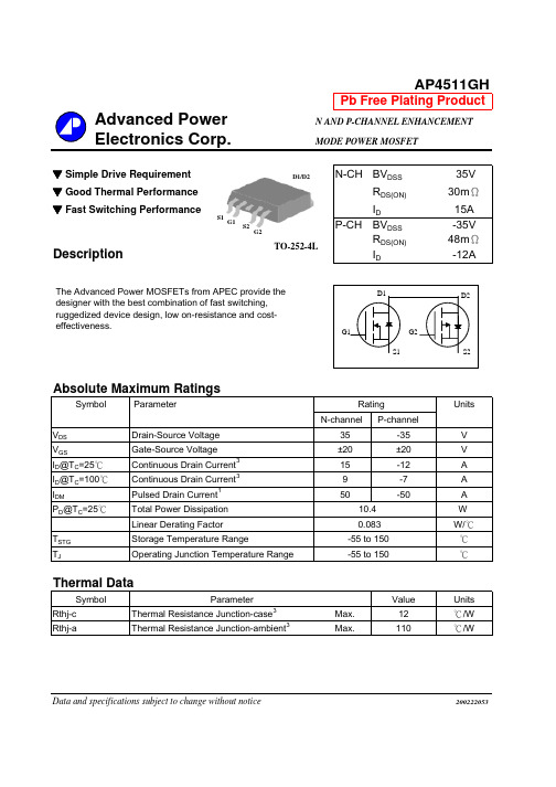
AP4511GH资料
25
Q G , Total Gate Charge (nC)
Fig 7. Gate Charge Characteristics
100
100us
10
ID (A)
1
T C =25 o C Single Pulse
1ms
10ms 100ms
DC
0.1
0.1
1
10
100
V DS , Drain-to-Source Voltage (V)
Parameter Forward On Voltage2 Reverse Recovery Time2
Reverse Recovery Charge
Test Conditions IS=-6A, VGS=0V IS=-6A, VGS=0V dI/dt=-100A/µs
Min. Typ. Max. Units
BVDSS
ΔBVDSS/ΔTj
RDS(ON)
VGS(th) gfs IDSS
IGSS Qg Qgs Qgd td(on) tr td(off) tf Ciss Coss Crss Rg
Drain-Source Breakdown Voltage VGS=0V, ID=250uA
Breakdown Voltage Temperature Coefficient Reference to 25℃, ID=1mA Static Drain-Source On-Resistance2 VGS=10V, ID=8A
Fig 6. Gate Threshold Voltage v.s. Junction Temperature
元器件交易网
N-Channel
14
CD4511BNSR;CD4511BPWR;CD4511BE;CD4511BPWRE4;CD4511BPWRG4;中文规格书,Datasheet资料
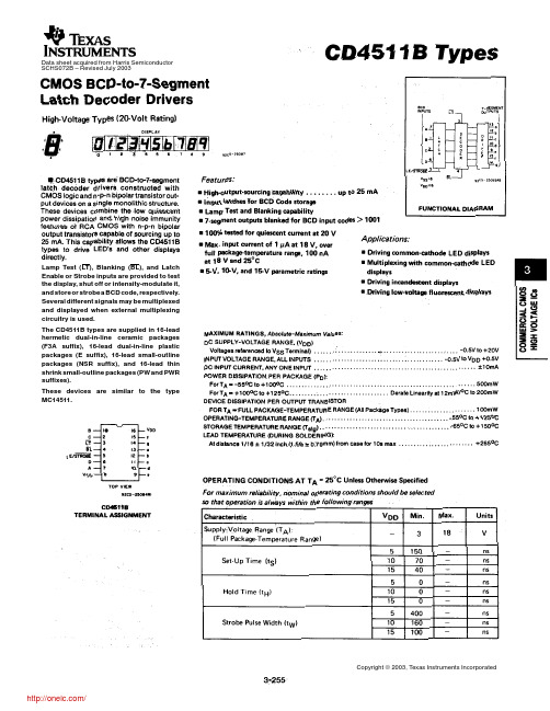
PACKAGING INFORMATIONOrderable Device Status(1)PackageType PackageDrawingPins PackageQtyEco Plan(2)Lead/Ball Finish MSL Peak Temp(3)CD4511BE ACTIVE PDIP N1625Pb-Free(RoHS)CU NIPDAU N/A for Pkg TypeCD4511BEE4ACTIVE PDIP N1625Pb-Free(RoHS)CU NIPDAU N/A for Pkg Type CD4511BF ACTIVE CDIP J161TBD A42N/A for Pkg Type CD4511BF3A ACTIVE CDIP J161TBD A42N/A for Pkg Type CD4511BNSR ACTIVE SO NS162000Green(RoHS&no Sb/Br)CU NIPDAU Level-1-260C-UNLIMCD4511BNSRE4ACTIVE SO NS162000Green(RoHS&no Sb/Br)CU NIPDAU Level-1-260C-UNLIMCD4511BNSRG4ACTIVE SO NS162000Green(RoHS&no Sb/Br)CU NIPDAU Level-1-260C-UNLIMCD4511BPW ACTIVE TSSOP PW1690Green(RoHS&no Sb/Br)CU NIPDAU Level-1-260C-UNLIMCD4511BPWE4ACTIVE TSSOP PW1690Green(RoHS&no Sb/Br)CU NIPDAU Level-1-260C-UNLIMCD4511BPWG4ACTIVE TSSOP PW1690Green(RoHS&no Sb/Br)CU NIPDAU Level-1-260C-UNLIMCD4511BPWR ACTIVE TSSOP PW162000Green(RoHS&no Sb/Br)CU NIPDAU Level-1-260C-UNLIMCD4511BPWRE4ACTIVE TSSOP PW162000Green(RoHS&no Sb/Br)CU NIPDAU Level-1-260C-UNLIMCD4511BPWRG4ACTIVE TSSOP PW162000Green(RoHS&no Sb/Br)CU NIPDAU Level-1-260C-UNLIM(1)The marketing status values are defined as follows:ACTIVE:Product device recommended for new designs.LIFEBUY:TI has announced that the device will be discontinued,and a lifetime-buy period is in effect.NRND:Not recommended for new designs.Device is in production to support existing customers,but TI does not recommend using this part in a new design.PREVIEW:Device has been announced but is not in production.Samples may or may not be available.OBSOLETE:TI has discontinued the production of the device.(2)Eco Plan-The planned eco-friendly classification:Pb-Free(RoHS),Pb-Free(RoHS Exempt),or Green(RoHS&no Sb/Br)-please check /productcontent for the latest availability information and additional product content details.TBD:The Pb-Free/Green conversion plan has not been defined.Pb-Free(RoHS):TI's terms"Lead-Free"or"Pb-Free"mean semiconductor products that are compatible with the current RoHS requirements for all6substances,including the requirement that lead not exceed0.1%by weight in homogeneous materials.Where designed to be soldered at high temperatures,TI Pb-Free products are suitable for use in specified lead-free processes.Pb-Free(RoHS Exempt):This component has a RoHS exemption for either1)lead-based flip-chip solder bumps used between the die and package,or2)lead-based die adhesive used between the die and leadframe.The component is otherwise considered Pb-Free(RoHS compatible)as defined above.Green(RoHS&no Sb/Br):TI defines"Green"to mean Pb-Free(RoHS compatible),and free of Bromine(Br)and Antimony(Sb)based flame retardants(Br or Sb do not exceed0.1%by weight in homogeneous material)(3)MSL,Peak Temp.--The Moisture Sensitivity Level rating according to the JEDEC industry standard classifications,and peak solder temperature.Important Information and Disclaimer:The information provided on this page represents TI's knowledge and belief as of the date that it is provided.TI bases its knowledge and belief on information provided by third parties,and makes no representation or warranty as to the accuracy of such information.Efforts are underway to better integrate information from third parties.TI has taken and continues to take reasonable steps to provide representative and accurate information but may not have conducted destructive testing or chemical analysis on incoming materials and chemicals.TI and TI suppliers consider certain information to be proprietary,and thus CAS numbers and other limited information may not be available for release.In no event shall TI's liability arising out of such information exceed the total purchase price of the TI part(s)at issue in this document sold by TI to Customer on an annual basis.TAPE AND REEL INFORMATION*All dimensions are nominalDevicePackage Type Package Drawing Pins SPQReel Diameter (mm)Reel Width W1(mm)A0(mm)B0(mm)K0(mm)P1(mm)W (mm)Pin1Quadrant CD4511BNSR SO NS 162000330.016.48.210.5 2.512.016.0Q1CD4511BPWRTSSOPPW162000330.012.46.95.61.68.012.0Q1*All dimensions are nominalDevice Package Type Package Drawing Pins SPQ Length(mm)Width(mm)Height(mm) CD4511BNSR SO NS162000367.0367.038.0CD4511BPWR TSSOP PW162000367.0367.035.0分销商库存信息:TICD4511BNSR CD4511BPWR CD4511BECD4511BPWRE4CD4511BPWRG4CD4511BNSRE4 CD4511BNSRG4CD4511BEE4CD4511BPW CD4511BPWE4CD4511BPWG4。
4511GM

-
9
-
S
-
- -1 uA
-
- -25 uA
-
- ±100 nA
- 10 16 nC
-
2
- nC
-
6
- nC
- 10 - ns
-
6
- ns
- 26 - ns
-
7
- ns
- 690 1100 pF
- 165 - pF
- 130 - pF
- 5.2 7.8 Ω
Source-Drain Diode
Symbol VSD trr Qrr
The SO-8 package is universally preferred for all commercialindustrial surface mount applications and suited for low voltage applications such as DC/DC converters.
50
T A = 150 o C
40
30
20
10V 7.0V 5.0V
4.5V
10
V G =3.0V
0
0
1
2
3
4
5
V DS , Drain-to-Source Voltage (V)
Fig 2. Typical Output Characteristics
1.8
1.6
ID=7A
V G =10V
1.4
1.2
Min. Typ. Max. Units
-
- 1.2 V
- 18 - ns
- 12 - nC
AP4511GM
CD4511中文资料

A→Y
-
BI → Y
-
BI → Y
-
LT → Y LT → Y
-
tTHL 传输转换时间
-
tTLH 传输转换时间
-
tW LE 脉冲宽度
400 160 100 150 70 40 0 0 0
tSU 建立时间
-
ns
tH 保持时间
-
ns
C1 输入电容 (任一输入端)
7.5
pF
动态特性(TA=25℃) : 参数 tPLH 传输延 迟时间 tPHL 传输延 迟时间 tPLH 传输延 迟时间 tPHL 传输延 迟时间 tPLH 传输延 迟时间 tPHL 传输延 迟时间 A→Y 测试条件 CL=50pF RL=200k tr=20ns tf=20ns VDD(V) 最小 5.0 10.0 15.0 5.0 10.0 15.0 5.0 10.0 15.0 5.0 10.0 15.0 5.0 10.0 15.0 5.0 10.0 15.0 5.0 10.0 15.0 5.0 10.0 15.0 5.0 10.0 15.0 5.0 10.0 15.0 规范值 最大 1040 420 300 800 350 300 700 350 250 300 150 100 500 250 170 310 185 160 100 75 65 ns ns ns 单位
BI
LE
输出消隐控制端 数据锁定控制 灯测试 正电源 地 数据输出端
LT
VDD Vss Ya~Yg 功能表
静态特性: 参数 IoH (mA) VOL 输出低电 平电压 (最大) VOH 输出高电 平电压 (最小) VIL 输入低电平 电压 (最大) VIH 输入高电平 电压 (最小) VOH 输出高电 平驱动电压 (最小) 测试条件 V0 (V) V1 (V) 5/0 10/0 15/0 5/0 10/0 15/0 VDD (V) 5.0 10.0 15.0 5.0 10.0 15.0 5.0 10.0 15.0 5.0 10.0 15.0 5.0 4.0 3.8 -3.55 3.4 9.0 8.85 8.7 8.6 14.0 13.9 13.75 13.65 0.64 1.6 4.2 5.0 10.0 20.0 0.61 1.5 4.0 ±0.1 5.0 10.0 20.0 4.0 9.0 14.0 -55℃ -40℃ 规范值 25℃ 0.05 85℃ 125℃ 单 位 V
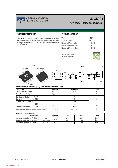
AO4821;中文规格书,Datasheet资料
100% UIS Tested 100% Rg TestedSymbol V DS V GSI DM T J , T STGSymbolt ≤ 10s Steady-State Steady-StateR θJLW 2Maximum Junction-to-Lead°C/W°C/W Maximum Junction-to-Ambient A D 329040Maximum Junction-to-Ambient A T A =25°C T A =70°C Power DissipationBP D Pulsed Drain Current CContinuous Drain CurrentT A =25°C AI D -9-7-60V MaximumUnits Parameter Absolute Maximum Ratings T A =25°C unless otherwise noted V ±8Gate-Source Voltage Drain-Source Voltage -12°C/W R θJA 487462.5°CThermal Characteristics Units ParameterTyp Max 1.28T A =70°CJunction and Storage Temperature Range -55 to 150G1S1G2S2D1D1D2D224513867 Top ViewSOIC-8Top View Bottom ViewPin1G1D11S1RgG2D2S2RgSymbolMin Typ Max Units BV DSS -12VV DS =-12V, V GS =0V-1T J =55°C-5I GSS ±10µA V GS(th)Gate Threshold Voltage -0.35-0.53-0.85V I D(ON)-60A 1619T J =125°C22271924m Ω2330m Ωg FS 45S V SD -0.56-1V I S-3A C iss 139017402100pF C oss 230334435pF C rss 120200280pF R g0.9 1.3 1.7k ΩQ g (4.5V)151923nC Q gs 3.6 4.5 5.4nC Q gd 35.37.4nC t D(on)240ns t r 580ns t D(off)7µs t f 4.2µst rr 182226ns Q rr141720nCTHIS PRODUCT HAS BEEN DESIGNED AND QUALIFIED FOR THE CONSUMER MARKET. APPLICATIONS OR USES AS CRITICAL COMPONENTS IN LIFE SUPPORT DEVICES OR SYSTEMS ARE NOT AUTHORIZED. AOS DOES NOT ASSUME ANY LIABILITY ARISING OUT OF SUCH APPLICATIONS OR USES OF ITS PRODUCTS. AOS RESERVES THE RIGHT TO IMPROVE PRODUCT DESIGN,FUNCTIONS AND RELIABILITY WITHOUT NOTICE.Body Diode Reverse Recovery TimeDrain-Source Breakdown Voltage On state drain currentI D =-250µA, V GS =0V V GS =-4.5V, V DS =-5V V GS =-4.5V, I D =-9AReverse Transfer Capacitance I F =-9A, dI/dt=500A/µsV GS =0V, V DS =-6V, f=1MHz SWITCHING PARAMETERS Electrical Characteristics (T J =25°C unless otherwise noted)STATIC PARAMETERS ParameterConditions I DSS µA V DS =V GS I D =-250µA V DS =0V, V GS = ±8V Zero Gate Voltage Drain Current Gate-Body leakage current Forward Transconductance Diode Forward VoltageR DS(ON)Static Drain-Source On-Resistancem ΩI S =-1A,V GS =0VV DS =-5V, I D =-9A V GS =-1.8V, I D =-6AV GS =-2.5V, I D =-8A Gate resistanceV GS =0V, V DS =0V, f=1MHzTurn-Off Fall TimeTotal Gate Charge V GS =-4.5V, V DS =-6V, I D =-9AGate Source Charge Gate Drain Charge Body Diode Reverse Recovery Charge I F =-9A, dI/dt=500A/µsMaximum Body-Diode Continuous CurrentInput Capacitance Output CapacitanceTurn-On DelayTime DYNAMIC PARAMETERS Turn-On Rise Time Turn-Off DelayTime V GS =-4.5V, V DS =-6V, R L =0.67Ω,R GEN =3ΩA. The value of R θJA is measured with the device mounted on 1in 2FR-4 board with 2oz. Copper, in a still air environment with T A =25°C. The value in any given application depends on the user's specific board design.B. The power dissipation P D is based on T J(MAX)=150°C, using ≤ 10s junction-to-ambient thermal resistance.C. Repetitive rating, pulse width limited by junction temperature T J(MAX)=150°C. Ratings are based on low frequency and duty cycles to keep initialT J =25°C.D. The R θJA is the sum of the thermal impedence from junction to lead R θJL and lead to ambient.E. The static characteristics in Figures 1 to 6 are obtained using <300µs pulses, duty cycle 0.5% max.F. These curves are based on the junction-to-ambient thermal impedence which is measured with the device mounted on 1in 2 FR-4 board with 2oz. Copper, assuming a maximum junction temperature of T J(MAX)=150°C. The SOA curve provides a single pulse ratin g.TYPICAL ELECTRICAL AND THERMAL CHARACTERISTICS5101520Q g (nC)Figure 7: Gate-Charge Characteristics-V G S (V o l t s )24681012-V DS (Volts)Figure 8: Capacitance Characteristics C a p a c i t a n c e (p F )VdsCharge Gate Charge Test Circuit & WaveformD iode RVVddVddVR esistive S w itching Test C ircuit & W aveform s分销商库存信息: AOSAO4821。