锁相环中的相位噪声研究
第2.6章 锁相环路的噪声性能

因此,本章节的分析方法称为环路在弱噪声作用下的线性分析。
3
2.6.1 输入加性噪声的特性
锁相环输入噪声常常是经过环路前的选择性回路才加到输入端的, 其选择性回路的带宽远小于中心频率,即 B f0 。
当噪声通过选择性回路,形成一个振幅和相位都作随机变化的高频 噪声。统计分析表明,这种噪声具有窄带高斯白噪声性质。
增大K 时,BL 随之也增大,很难满足多方面性能需求,故很少应用。
20
2.6.3 环路对输入噪声的线性过滤
(2)各种锁相环的相位噪声带宽 采用无源比例积分滤波器的二阶环噪声带宽为:
BL
n 8
1
2
n
K
2
当
K
n
时,近似为:
BL
n 8
N
t
由上式,得到下面的加性噪声输入时的环路相位模型 。
14
2.6.3 环路对输入噪声的线性过滤
(一)环路等效输入相位噪声
在弱噪声作用下,即相位差 e t 的均方根值 e 13o 时, 环路相
位误差 et 300 的概率近似为1,可将 sine e ,使方程线性化,
0 f B 2
9
2.6.2 输入加性噪声的环路相位模型
在已知环路输入噪声性质的基础上,可以获得环路的相位模型。 当有输入加性噪声时,加在环路输入端的电压是信号与噪声之和,即:
Vi t nt Vi sin0t 1t nc tcos0t ns tsin 0t
(2)各种锁相环的相位噪声带宽 采用不同滤波器的环路,其闭环频率响应不同,因此计算出的相
锁相环中相位噪声的确定
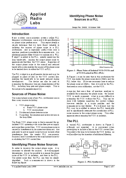
output impedance is only really correct for active loop filters, if passive filters are used then the widget design is complicated by the need to use a low-noise buffer amplifier. We will not consider this case here. Choosing some convenient values (not particularly critical) R1 = 100k , R2 = 1k and C 2 = 10 µF gives a pole at 0.16Hz and a zero at 16Hz. The response is shown in Figure 5:
The PLL
A typical PLL synthesiser is shown in Figure 2. Although not essential, it is convenient when prototyping to include a link on the VCO control line. This allows the loop to be broken for VCO testing, as well as allowing the insertion of additional filtering.
锁相环电路的设计及相位噪声分析
和响应速度之间折衷考虑,相位裕度越大,系统越稳定,但是响应速度变慢。
这里取相位裕度为60度。
同样的,这两个环路参数是估计出来的,在实际电路中仍然需要多次考虑。
最后根据上面的两个环路参数,利用第二章第六节的公式2-22到2-24可以计算出低通滤波器的电阻和电容的值大约为:R2=12K,C2=138PF,CI=1IPF。
根据以上估算的参数可以将锁相环系统的幅频和相频特性曲线画出,如图4.2所示。
图4-2PLL的幅频与相频特性曲线4.3锁相环系统级模型4.3.1Matlab构造数学模型Mauab是MathWorks公司开发的具有强大科学运算功能的数学工具,其中的软件包--Simulink是专门用于数学建模的工具。
通过建立锁相环系统的线性模型,如图4—3所示,分别建立环路中每个模块的传输函数,然后设置输入输出点。
该线性模型不仅可以分析系统的冲击响应和阶跃响应,还可以分析零极点与波特图。
冲击响应和阶越响应的模拟结果如图4-4所示,此模型可以很方便的修改参数,仿真速度非常快,模拟结果也非常直观,对于理解二阶系统的特性非常有帮助。
t№啦*血瞻呻目删e,ra口aap蝌m鼬rtrartim'哥缸眦h恤啪蚓of恤VCO图4-3Matlab建立PLL的线性模型图4—4PLL的阶跃响应与冲击响应4.3.2VerilogA构造行为级模型VerilogA语言是Verilog硬件描述语言的扩展,主要用来描述模拟系统的结构和行为,包括电子,机械,流体力学和热力学系统等㈣。
下面给出VerilogA描述锁相环的行为级模型,并应用Mica进行仿真。
首先,以电阻的行为级模型为例,简单的说明一下VerilogA语言的特点和应用。
、include“disciplines.”’’include“constants.h,’moduleres(a,b);inouta,b;electricala,b;parameterrealR21.O:analogbeginI(a,b)<+V(a,b)/R;//Altemative:V(a,b)<+I(a,b)4R;第五章锁相环电路设计及模拟第五章锁相环电路设计及模拟5.1整体设计本章主要是关于锁相环的晶体管级电路的设计,不但详细的分析了电路的结构,而且给出了模拟结构及相关的解释。
锁相频率源混频信号的相位噪声分析
锁相频率源混频信号的相位噪声分析为了研究锁相频率源的混频信号的相位噪声问题,本文将锁相源的相位噪声构成作为基础,构建起两路相关锁相源混频相位噪声近似数学模型,并开展了相关实验。
实验数据表明,模型仿真能够得到与实验一致的结果,可以在很大程度上降低相位噪声估值偏差。
标签:锁相频率源;混频信号;相位噪声1 相位噪声概述通常来讲,信号频率或者相位本身的短期性、随机性起伏是引发相位噪声的主要原因,理想的频率源信号得到的频谱近似直线,数学上一般用带有幅度的Delta函数表示。
而从实际测量的角度,频谱信号两侧可以看到宽度较大的连续分布谱,其形成的原因是热能与其他噪声源随机起伏对于频率信号的调整,这里的连续分布谱实际上就是相位噪声。
假定θ(t)表示噪声形成的调制信号,考虑到相位噪声同样属于较小的信号调制,满足θ(t)《1,可以将频率源信号表示为:(1)公式中,fc表示载波信号,对于公式进行相应的Fourier变换,可以得到(2)这里的S(f)表示S(t)的Fourier頻率谱,Sθ=F(θ(t)),表示相位与频率抖动的功率谱密度。
结合上述公式,参考相位噪声的内涵,可以通过分贝值的形式来对频率源相位噪声进行表示,有(3)公式中,=f-fc,该公式实际上是偏离载波位置1Hz带宽的相位噪声。
调制信号本身属于非平稳性的随机过程,而结合相应的文献研究以及工程实践,可以将其近似看做是平稳的高斯过程,能够得到近乎实际工程值的结果。
设相应的高斯过程θ(t)为N(0,),均值E=0,相位与频率会于载波信号附近抖动。
方差表示为相位噪声的功率,依照上述公式,可以得到相应的公式(4)2 锁相频率源相位噪声结构就目前而言,比较常见的锁相源一般都是有压控振荡器、鉴相器、环路滤波器以及分频器等构成,所有元器件的噪声都会影响最终输出频率的相位噪声,而其中最为关键,最不可避免的,是鉴相器鉴相基底倍频以及参考信号锁相倍频的恶化。
参考公式(4),可以将锁相源相位噪声表示为(5)在公式中,表示锁相源最终输出的相位噪声功率,和分别表示晶振锁相倍频恶化以及鉴相基底倍频恶化后的相位噪声功率,结合上述分析,参照公式(4)和公式(5),可以将相位噪声改写成分贝值的形式,得到锁相源相位噪声计算公式:(6)3 加入混频器后的相位噪声分析理想状态下,混频器的输出包含了两个输入信号的和频与差频,而实际上,混频器具备多个交调分量,不过和频与差频是主要分量。
锁相跳频源相位噪声预测方法的研究
・ 0・ 8
兵 工 自动 化
第 3 卷 1
晶 振 对 应 的 噪 声 传 递 函 数 为 式 () 4:
,
一
振 荡器 、 相器 、 分频器和 R分频器噪 声的大小 ; 鉴 N
() 4
() 1
I I l十
G ()
U l I 仃 I l .
而 带 外 (3 ) 0> 的相 位 噪 声 要 取 决 于 VC 的 相 O
2 20 01 . 2
Or na c nd s r t m a i n d n e I u t y Au o to
兵 工 自 动 化
・7 ・ 9
3 () 12
锁 相跳 频 源相 位 噪 声预 测 方法 的研 究
彭 永 怀 , 周 雷 ,冯 江 华
( .总 装 驻 绵 阳 地 区 军 代 室 , 四 』I绵 阳 6 1 0 ; 2 1 I 2 0 0 .四 川 九 洲 电器 集 团 有 限 责 任 公 司 , 四 川 绵 阳 6 1 0 ) I 2 0 0o N (2 1)
由 式 () 5 、( )可 以看 出 ,鉴 相 器 、R 分 频 4 、( ) 6 器 、 N 分 频 器 和 参 考 晶 振 的噪 声 传 递 函 数 有 一 个 共
同的 闪予: ,这 是 它 们 与 VC 噪 声 传 O
Ke r s p aelc e o ;rq e c y teie; h s os; rq e c mps nh s e ywo d : h s o k dl p fe u n ysnh szr p a e ie f u n yj y tei r o n e u z
O 引 言
相 位 噪 声 是 影 响现 代 通 信 系 统 灵 敏 度 和 选 择 性
锁相环的相位噪声分析

锁相环路相位噪声分析张文军 电信0802【摘要】本文对锁相电路的相位噪声进行了论述,并对其中各组成部件的相位噪声也做了较为详细的分析。
文中最后提出了改进锁相环相位噪声的办法。
【关键词】锁相环;相位噪声;分析 引言相位噪声是一项非常重要的性能指标,它对电子设备和电子系统的影响很大,从频域看它分布的载波信号两旁按幂律谱分布。
用这种信号无论做发射激励信号,还是接收机本振信号以及各种频率基准,这些信号在解调过程中都会和信号一样出现在解调终端,引起基带信噪比下降。
在通信系统中使环路信噪比下将,误码率增加;在雷达系统中影响目标的分辨能力,即改善因子。
接收机本振的相位噪声遇到强干扰信号时,会产生“倒混频”,使接收机有效噪声系数增加。
随着电子技术的发展,对频率源的信号噪声要求越来越严格,因此低相位噪声在物理、天文、无线电通信、雷达、航空、航天以及精密计量、仪器仪表等各种领域里都受到重视。
1 相位噪声概述相位噪声 ,就是指在系统内各种噪声作用下所表现的相位随机起伏,相位的随机起伏起必然引起频率随机起伏,这种起伏速度较快,所以又称之为短期频率稳定度。
理想情况下,合成器的输出信号在频域中为根单一的谱线,而实际上任何信号的频谱都不可能绝对纯净,总会受到噪声的调制产生调制边带。
由于相位噪声的存在,使波形发生畸变。
在频域中其输出信号的谱线就不再是一条单根的谱线,而是以调制边带的形式连续地分布在载波的两边,在主谱两边出现了一些附加的频谱,从而导致频谱的扩展,相位噪声的边带是双边的,是以0f 为中心对称的,但为了研究方便,一般只取一个边带。
其定义为偏离载频1Hz带宽内单边带相位噪声的功率与载频信号功率之比,它是偏离 载频的复氏频率m f 的函数 ,记为()m f ζ,单位为d B c / Hz ,即()010lg[/](1)m SSB f P P ζ=式中SSB P 为偏离载频m f 处,1Hz 带宽内单边带噪声功率;0P 为载波信号功率。
锁相环输出信号相位噪声噪声及杂散特性分析应用实践
锁相环输出信号相位噪声噪声及杂散特性分析应用实践【摘要】本文详细地介绍了锁相环的鉴频鉴相器、分频器和输入参考信号的相位噪声对锁相环合成输出信号的近端相位噪声的具体贡献值。
并以CDMA 1X基站系统中800MHz的FS 单板的锁相环输出信号相位噪声指标进行理论计算。
为广大锁相环设计者提供理论计算方法的参考和实践设计的参考依据。
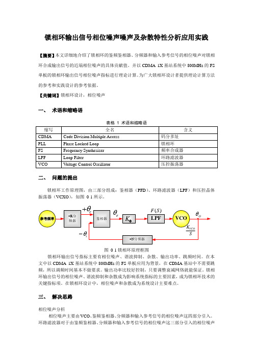
【关键词】锁相环设计,相位噪声一、术语和缩略语表格 1 术语和缩略语二、问题的提出锁相环工作原理图,由三部分组成:鉴相器(PFD)、环路滤波器(LPF)和压控晶体振荡器(VCXO),如图0-1所示。
图0-1锁相环原理框图锁相环输出信号指标主要有相位噪声、谐波抑制、杂散、输出功率、跳频时间。
在本文中以CDMA 1X基站系统中800MHz的FS单板应用为背景,在CDMA基站中不需要跳频,所以调频时间基本不做要求。
输出功率比较好控制,只要调整衰减网络就能保证。
锁相环输出信号的相位噪声、谐波抑制和杂散成为影响系统指标的主要因素,成为锁相环技术的关键指标项。
在锁相环设计中,相位噪声和杂散成为系统设计主要难点。
三、解决思路相位噪声分析相位噪声主要由VCO、鉴频鉴相器、分频器和输入参考信号的相位噪声这四部分引入。
环路滤波器对于由鉴频鉴相器、分频器和输入参考信号的相位噪声这三部分引入的相位噪声具有低通特性,对于VCO产生的相位噪声具有高通特性。
一般来说环路带宽内的相位噪声主要决定于由鉴频鉴相器、分频器和输入参考信号,环路带宽以外的相位噪声主要决定于VCO,在环路带宽周围,这四部分的噪声影响相当。
所以为了尽量降低输出信号的相位噪声环路滤波器的环路带宽的最佳点是由鉴频鉴相器、分频器和输入参考信号的相位噪声这三部分引入的相位噪声总和与VCO引入的相位噪声相同时的频率。
在实际运用中还礼滤波器的设计是非常重要的。
对于远端相位噪声如100KHz和1MHz处的一般远远高于环路带宽,其相位噪声主要决定于VCO,要保证其指标主要是选择良好的VCO。
相位噪声基础及测试原理和方法
摘要:相位噪声指标对于当前的射频微波系统、移动通信系统、雷达系统等电子系统影响非常明显,将直接影响系统指标的优劣。
该项指标对于系统的研发、设计均具有指导意义。
相位噪声指标的测试手段很多,如何能够精准的测量该指标是射频微波领域的一项重要任务。
随着当前接收机相位噪声指标越来越高,相应的测试技术和测试手段也有了很大的进步。
同时,与相位噪声测试相关的其他测试需求也越来越多,如何准确的进行这些指标的测试也愈发重要。
1、引言随着电子技术的发展,器件的噪声系数越来越低,放大器的动态范围也越来越大,增益也大有提高,使得电路系统的灵敏度和选择性以及线性度等主要技术指标都得到较好的解决。
同时,随着技术的不断提高,对电路系统又提出了更高的要求,这就要求电路系统必须具有较低的相位噪声,在现代技术中,相位噪声已成为限制电路系统的主要因素。
低相位噪声对于提高电路系统性能起到重要作用。
相位噪声好坏对通讯系统有很大影响,尤其现代通讯系统中状态很多,频道又很密集,并且不断的变换,所以对相位噪声的要求也愈来愈高。
如果本振信号的相位噪声较差,会增加通信中的误码率,影响载频跟踪精度。
相位噪声不好,不仅增加误码率、影响载频跟踪精度,还影响通信接收机信道内、外性能测量,相位噪声对邻近频道选择性有影响。
如果要求接收机选择性越高,则相位噪声就必须更好,要求接收机灵敏度越高,相位噪声也必须更好。
总之,对于现代通信的各种接收机,相位噪声指标尤为重要,对于该指标的精准测试要求也越来越高,相应的技术手段要求也越来越高。
2、相位噪声基础2.1、什么是相位噪声相位噪声是振荡器在短时间内频率稳定度的度量参数。
它来源于振荡器输出信号由噪声引起的相位、频率的变化。
频率稳定度分为两个方面:长期稳定度和短期稳定度,其中,短期稳定度在时域内用艾伦方差来表示,在频域内用相位噪声来表示。
2.2、相位噪声的定义以载波的幅度为参考,在偏移一定的频率下的单边带相对噪声功率。
这个数值是指在1Hz的带宽下的相对噪声电平,其单位为dBc/Hz。
- 1、下载文档前请自行甄别文档内容的完整性,平台不提供额外的编辑、内容补充、找答案等附加服务。
- 2、"仅部分预览"的文档,不可在线预览部分如存在完整性等问题,可反馈申请退款(可完整预览的文档不适用该条件!)。
- 3、如文档侵犯您的权益,请联系客服反馈,我们会尽快为您处理(人工客服工作时间:9:00-18:30)。
The Research of Noise in The PLLLU Shiqiang , YANG Guoyu( School of the Microwave engineering ,UESTC ChengDu 610054 China ) Absract This articles introducs the basic concepts and the phase noise in phase-locked loops (PLLs). It focus on a detailed examination of two critical specifications associated with PLLs : phase noise and reference spurs. What causes them and how can they be minimized? Also it inculdes an example .Key words :PLL ; Phase Noise ; Oscillator1 . The Basic Theory of the PLLA phase-locked loop is a feedback system combining a voltage controlled oscillator and a phase comparator so connected that the oscillator maintains a constant phase angle relative to a reference signal. Phase-locked loops can be used, for example, to generate stable output frequency signals from a fixed low-frequency signal . The phase locked loop can be analyzed in general as a negative feedback system with a forward gain term and a feedback term. .A simple block diagram of a voltage-based negative-feedback system is shown in Figure 1.Figure 1. Standard negative-feedback control system model In a phase-locked loop, the error signal from the phase comparator is proportional to the relative phase of the input and feedback signals. The average output of the phase detector will be constant when the input and feedback signals are the same frequency. The usual equations for a negative-feedback system apply.Forward Gain = G(s), [s = jw = j2pif]Loop Gain = G(s) H(s)Closed Loop Gain = G(s)/[1+G(s)H(s)]Because of the integration in the loop, at low frequencies the steady state gain, G(s) is very high and VO/VI, Closed-Loop Gain =1/ H and Fo=NF REF. .The components of a PLL that contribute to the loop gain include :1. The phase detector (PD) and charge pump (CP).2. The loop filter, with a transfer function of Z(s)3. The voltage-controlled oscillator (VCO), with a sensitivity of KV /s4. The feedback divider, 1/NFigure 2 Basic phase-locked-loop modelThe following equations have be developed for the the error signal, Error Detector e(s)=ΦREF –Φ0/N , de(s)/dt=F REF –F0/NWhen e(s) =constant, F0/N = F REFThus F0 / N = F REF .In commercial PLLs , the phase detector and charge pump together form the error detector block. When F0/N≠F REF, the error detector will output source/sink current pulses to the low-pass loop filter. This smooths the current pulses into a voltage which in turn drives the VCO. The charge pump and VCO thus serves as an integrator , seeking to increase or decrease its output frequency to the value required so as to restore its input (from the phase detector) to zero.The loop filter is a low-pass type, typically with one pole and one zero. The transient response of the loop depends on:1. the magnitude of the pole/zero,2. the charge pump magnitude,3. the VCO sensitivity,4. the feedback factor, N.In addition, the filter must be designed to be stable (usually a phase margin of pi/4 is recommended).The 3-dB cutoff frequency of the response is usually called the loop bandwidth, BW. Large loop bandwidths result in very fast transient response . However, this is not always advantageous, and there is a tradeoff between fast transient response and reference spur attenuation.2. Noise in the OsillatorBefore we look at phase noise in a PLL system, it is worth considering the phase noise in a voltage-controlled oscillator (VCO).2.1 Noise in Oscillator SystemsIn any oscillator design, frequency stability is of critical importance. We are interested in both long-term and short-term stability. Long-term frequency stability is concerned with how the output signal varies over a long period of time (hours, days or months). It is usually specified as the ratio, Df/f for a given period of time, expressed as a percentage or in dB. Short-term stability, on the other hand, is concerned with variations that occur over a period of seconds or less.These variations can be random or periodic. A spectrum analyzer can be used to examine the short-term stability of a signal. Figure 1 shows a typical spectrum, with random and discrete frequency components causing a broad skirt and spurious peaks.Figure 1 Short-term stability in oscillatorsThe discrete spurious components could be caused by known clock frequencies in the signal source, power line interference, and mixer products. The broadening caused by random noise fluctuation is due to phase noise. It can be the result of thermal noise, shot noise and/or flicker noise in active and passive devices.2.2 Phase noise in VCO (Voltage Control Oscillator )Figure 2 Phase representation of phase noiseA signal of angular velocity w0 and peak amplitude VSPK is shown. Superimposed on this is an error signal of angular velocity wm. Dqrms represents the rms value of the phase fluctuations and is expressed in rms degrees. In many radio systems, an overall integrated phase error specification must be met. This overall phase error is made up of the PLL phase error, the modulator phase error and the phase error due to base band components. In GSM, for example, the total allowed is 5 degrees rms.Leeson’s EquationLeeson developed an equation to describe the different noise components in a VCO.where:LPM is single-sideband phase noise density (dBc/Hz)F is the device noise factor at operating power level A (linear)k is Boltzmann’s constant, 1.38E-23 J/KT is temperature (K)A is oscillator output power (W)Q l is loaded Q (dimensionless)f0 is the oscillator carrier frequencyf m is the frequency offset from the carrierFor Leeson’s equation to be valid, the following must be true:1.fm, the offset frequency from the carrier, is greater than the 1/f flicker corner frequency;2.the noise factor at the operating power level is known;3.the device operation is linear;4.Q includes the effects of component losses, device loading and buffer loading;Figure 3 Phase noise in a VCO vs frequency offsetLeeson’s equation only applies in the knee region between the break (f1) to the transition from the “1/f ” (more generally 1/fg ) flicker noise frequency to a frequency beyond which amplified white noise dominates (f2). This is shown in Figure 3 [g = 3]. f1 should be as low as possible; typically, it is less than 1 kHz, while f2 is in the region of a few MHz. High-performance oscillators require devices specially selected for low 1/f transition frequency. Some guidelines to minimizing the phase noise in VCOs are:1. Keep the tuning voltage of the varactor sufficiently high (typically between 3 and 3.8 V)2. Use filtering on the dc voltage supply.3. Keep the inductor Q as high as possible. Typical off-the-shelf coils provide a Q of between50 and 60.4. Choose an active device that has minimal noise figure as well as low flicker frequency.The flicker noise can be reduced by the use of feedback elements.5. Most active device exhibit a broad U-shaped noise-figure-vs.-bias-current curve. Use thisinformation to choose the optimal operating bias current for the device.6. Maximize the average power at the tank circuit output.7. When buffering the VCO, use devices with the lowest possible noise figure.3 . Phase noise of the VCO in the PLLHaving looked at phase noise in a free-running VCO and considered how it can be minimized, we will now consider the effect of closing the loop on phase noise.Figure4 PLL-phase-noise contributors in the PLLThe system transfer function may be described by the following equations.Closed Loop Gain = G/(1+GH) ;G= [ K d K v Z(s)] / s ;H= 1/N 。