开关型三端稳压器LM78Mxx-500系列数据手册 V1.1
78L05中文资料_数据手册_参数

LM78LXX系列三端正稳压器一般描述 LM78LXX系列三端正向稳压器是可用几个固定的输出电压使他们在广泛的应用中 有用.当用作齐纳二极管/电阻组合替代,LM78LXX usu-盟友导致有效的输出阻抗改善两个数量级以及更低的静态电流.这 些监管机构可以提供当地的卡规,消除与单点规则相关的分配问题 - 灰.可用电压允许LM78LXX用于逻辑系统,仪器仪 表,HiFi等固态电子设备. LM78LXX采用塑料TO-92(Z)封装,塑料SO-8(M)封装和芯片尺寸封装 (8-Bump micro SMD)采用美国国家半导体的微型SMD封装技术.如果有足够的散热片,肝脏100毫安输出电流.电流限制包括在内将峰 值输出电流限制在安全值.安全区域pro-提供对输出晶体管的检测以限制内部功耗.如果内部功耗变得太大高散热提供, 热关断CIR - cuit接管防止IC过热.特征 ? LM78L05采用微型SMD封装 ? 输出电压容差 在整个温度 范围内的 ± 5%范围 ?输 出电流100毫安 ?内部热过载保护 ?输出晶体管安全区域保护 ?内部短路电流限制 ?提供塑料TO-92和塑料SO-8低轮廓包 ?没 有外部元件 ?输出电压为5.0V,6.2V,8.2V,9.0V,12V,15V连接图 SO-8塑料(M) (窄体) DS007744-2顶视图 8凹凸 微型SMD DS007744-24顶视图 (凹凸面朝下) (TO-92)塑料包装(Z) DS007744-3底视图微型SMD标记方向 DS007744-33顶视图 可用性和规格.功耗(注5)内部限制输入电压 35V储存温度 -65?C至+150?C工作结温 SO-8 0?C至125?C微型SMD -40?C至 85?C焊接信息红外或对流(20秒) 235C波峰焊接(10秒) 260?C(提前期) ESD敏感度(注2)千伏 LM78LXX电气特性 标准字体的限制是T J =25?C,粗体字ap- SO-8封装的工作温度范围为0?C至125?C,微型SMD封装的工作温度范围为-40?C 至85?C.限制由产品保证,使用标准的统计质量控制(SQC)方法进行测试或相关技术.除非另有说明:I ? = 40毫安,C I =0.33μF,C0 =0.1μF. LM78L05除非另有规定,V IN = 10V符号参数条件敏典型马克斯单位 V ?输出电压 4.8五 5.2 V 7V ≤V IN≤20V 1毫安 ≤我 O≤40 mA (注3) 4.75 5.25 1毫安 ≤我 O≤70 mA (注3) 4.75 5.25 ΔV ?线路调整 7V ≤V IN≤20V 18 75毫伏 8V ≤V IN≤20V 10 54 ΔV ?负载调节 1毫安 ≤我 O≤100 mA 20 60 1毫安 ≤我 O≤40 mA五三十一世 Q 静态电流 3五 ΔI Q静态电流变化 8V ≤V IN≤20V 1.0 1毫安 ≤我 O≤40 mA 0.1 V ?输出噪声电压 f = 10Hz至100kHz (注 4) 40 μV波纹拒绝 f = 120Hz 8V ≤V IN≤16V 47 62 D b一世 PK峰值输出电流 140嘛平均输出电压温度系数一世 O = 5mA -0.65毫伏/℃ V IN (小)输入电压的小值保持线路规定所需 6.7 7 V θ JA热阻 (8凹凸微型SMD) 230.9 C / W LM78L62AC除非另有规定,V IN = 12V符号参数条件敏典型马克斯单位 V ?输出电压 5.95 .2 6.45 V 8.5V ≤V IN≤20V 1毫 安 ≤我 O≤40 mA (注3) 5.9 6.5 1毫安 ≤我 O≤70 mA (注3) 5.9 6
78,79系列三端稳压器器件资料

7805 790578XX系列集成稳压器的典型应用电路如下图所示,这是一个输出正5V直流电压的稳压电源电路。
IC采用集成稳压器7805,C1、C2分别为输入端和输出端滤波电容,RL为负载电阻。
当输出电较大时,7805应配上散热板。
下图为提高输出电压的应用电路。
稳压二极管VD1串接在78XX稳压器2脚与地之间,可使输出电压Uo得到一定的提高,输出电压Uo为78XX稳压器输出电压与稳压二极管VC1稳压值之和。
VD2是输出保护二极管,一旦输出电压低于VD1稳压值时,VD2导通,将输出电流旁路,保护7800稳压器输出级不被损坏。
下图为输出电压可在一定范围内调节的应用电路。
由于R1、RP电阻网络的作用,使得输出电压被提高,提高的幅度取决于R P与R1的比值。
调节电位器RP,即可一定范围内调节输出电压。
当RP=0时,输出电压Uo等于78XX稳压器输出电压;当RP逐步增大时,Uo也随之逐步提高。
下图为扩大输出电流的应用电路。
VT2为外接扩流率管,VT1为推动管,二者为达林顿连接。
R1为偏置电阻。
该电路最大输出电流取决于VT2的参数。
下图为提高输入电压的应用电路。
78XX稳压器的最大输入电压为35V(7824为40V),当输入电压高于此值时,可采用下图所示的电路。
VT、R1和VD组成一个预稳压电路,使得加在7800稳压器输入端的电压恒定在VD的稳压值上(忽略VT的b-e结压降)。
Ui端的最大输入电压仅取决于VT的耐压。
集成稳压器还可以用作恒流源。
下图为78XX稳压器构成的恒流源电路,其恒定电流Io等于78XX稳压器输出电压与R1的比值。
79XX系列集成压器是常用的固定负输出电压的三端集成稳压器,除输入电压和输出电压均为负值外,其他参数和特点与78XX系列集成稳压器相同。
79XX系列集成稳压的三个引脚为:1脚为接地端,2脚为输入端,3脚为输出端。
79XX系列集成稳压器的应用电路也很简单。
下图所示为输出-5V直流电压的稳压电源电路,IC采用集成稳压器7905,输出电流较大时应配上散热板。
78L05规格书

参数
输出电压
负载调整率
电压调整率 静态电流 静态电流变化量 输出噪声电压 输出电压温漂 纹波抑制比 输出电压降
测试条件 Tj=25°C 14.5V≤Vi≤27V;Io=1mA~40mA 14.5V≤Vi≤Vmax; Io=1mA~70mA Tj=25°C; Io=1mA~100mA Tj=25°C; Io=1mA~40mA Tj=25°C; 14.5V≤Vi≤27V Tj=25°C; 16V≤Vi≤27V
14.4
15 15.6
V
14.25 14.25
15.75
V
15.75 V (注 2)
20 150
mV
25 150
mV
25
150
mV
15
75
mV
2.2 6.5
mA
1.5
mA
0.1
mA
90
µV
-1.3
mV/°C
34
63
dB
1.7
V
绍兴芯谷科技有限公司
5/8
www. Silicore. com. cn
CHMC
16V≤Vi≤27V 1mA≤Io≤40mA 10Hz≤f≤100kHz Io=5mA 15V≤Vi≤25V; f=120Hz; Tj=25°C Tj=25°C
符号
Vo
∆Vo
∆Vo Iq ∆Iq VN ∆Vo/∆T RR Vd
最小值 典型值 最大值 单位
11.5
15
15.6
V
11.4
12.6
V
11.4
CHMC
Silicore
绍兴芯谷科技有限公司
78Lxx
极限值(绝对最大额定值,若无其它规定,Tamb=25℃)
LM7805中文资料
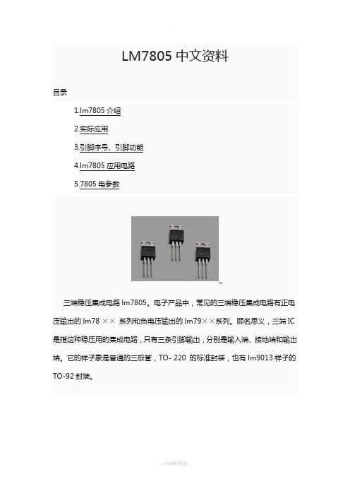
LM7805中文资料目录1.lm7805介绍2.实际应用3.引脚序号、引脚功能4.lm7805应用电路5.7805电参数三端稳压集成电路lm7805。
电子产品中,常见的三端稳压集成电路有正电压输出的lm78 ××系列和负电压输出的lm79××系列。
顾名思义,三端IC 是指这种稳压用的集成电路,只有三条引脚输出,分别是输入端、接地端和输出端。
它的样子象是普通的三极管,TO- 220 的标准封装,也有lm9013样子的TO-92封装。
1.lm7805介绍用lm78/lm79系列三端稳压IC来组成稳压电源所需的外围元件极少,电路内部还有过流、过热及调整管的保护电路,使用起来可靠、方便,而且价格便宜。
该系列集成稳压IC型号中的lm78或lm79后面的数字代表该三端集成稳压电路的输出电压,如lm7806表示输出电压为正6V,lm7909表示输出电压为负9V。
因为三端固定集成稳压电路的使用方便,电子制作中经常采用。
最大输出电流1.5A,LM78XX系列输出电压分别为5V;6V;8V;9V;10V;12V;15V;18V;24V。
2.实际应用在实际应用中,应在三端集成稳压电路上安装足够大的散热器(当然小功率7805IC内部电路图.的条件下不用)。
当稳压管温度过高时,稳压性能将变差,甚至损坏。
当制作中需要一个能输出1.5A以上电流的稳压电源,通常采用几块三端稳压电路并联起来,使其最大输出电流为N个1.5A,但应用时需注意:并联使用的集成稳压电路应采用同一厂家、同一批号的产品,以保证参数的一致。
另外在输出电流上留有一定的余量,以避免个别集成稳压电路失效时导致其他电路的连锁烧毁。
在lm78 ** 、lm79 ** 系列三端稳压器中最常应用的是TO-220 和TO-202 两种封装。
这两种封装的图形以及引脚序号、引脚功能如附图所示。
图中的引脚号标注方法是按照引脚电位从高到底的顺序标注的。
LM78LXX中文资料

LM78LXX Series3-Terminal Positive RegulatorsGeneral DescriptionThe LM78LXX series of three terminal positive regulators isavailable with several fixed output voltages making themuseful in a wide range of applications.When used as a zenerdiode/resistor combination replacement,the LM78LXX usu-ally results in an effective output impedance improvement oftwo orders of magnitude,and lower quiescent current.Theseregulators can provide local on card regulation,eliminatingthe distribution problems associated with single point regu-lation.The voltages available allow the LM78LXX to be usedin logic systems,instrumentation,HiFi,and other solid stateelectronic equipment.The LM78LXX is available in the plastic TO-92(Z)package,the plastic SO-8(M)package and a chip sized package(8-Bump micro SMD)using National’s micro SMD packagetechnology.With adequate heat sinking the regulator candeliver100mA output current.Current limiting is included tolimit the peak output current to a safe value.Safe areaprotection for the output transistors is provided to limit inter-nal power dissipation.If internal power dissipation becomestoo high for the heat sinking provided,the thermal shutdowncircuit takes over preventing the IC from overheating.Featuresn LM78L05in micro SMD packagen Output voltage tolerances of±5%over the temperaturerangen Output current of100mAn Internal thermal overload protectionn Output transistor safe area protectionn Internal short circuit current limitn Available in plastic TO-92and plastic SO-8low profilepackagesn No external componentsn Output voltages of5.0V,6.2V,8.2V,9.0V,12V,15Vn See AN-1112for micro SMD considerations Connection DiagramsSO-8Plastic(M)(Narrow Body)00774402Top View8-Bump micro SMD00774424Top View(Bump Side Down)(TO-92)Plastic Package(Z)00774403Bottom Viewmicro SMD Marking Orientation00774433Top ViewFebruary2005LM78LXXSeries3-TerminalPositiveRegulators ©2005National Semiconductor Corporation Ordering InformationPackageOrder Number Output VoltageNSC Drawing Supplied As microSMDLM78L05IBP5V BPA08AAB Reel of 250LM78L05IBPX 5V BPA08AAB Reel of 3000LM78L09ITP 9V TPA08AAA Reel of 250LM78L09ITPX9V TPA08AAA Reel of 3000SOIC NarrowLM78L05ACM 5V M08A Rail of 95LM78L05ACMX 5V M08A Reel of 2500LM78L12ACM 12V M08A Rail of 95LM78L12ACMX 12V M08A Reel of 2500LM78L15ACM 15V M08A Rail of 95LM78L15ACMX15V M08A Reel of 2500TO-92LM78L05ACZ 5V Z03A Box of 1800LM78L62ACZ 6.2V Z03A Box of 1800LM78L82ACZ 8.2V Z03A Box of 1800LM78L09ACZ 9V Z03A Box of 1800LM78L12ACZ 12V Z03A Box of 1800LM78L15ACZ15VZ03ABox of 1800L M 78L X X S e r i e s 2Absolute Maximum Ratings (Note 1)If Military/Aerospace specified devices are required,please contact the National Semiconductor Sales Office/Distributors for availability and specifications.Power Dissipation (Note 5)Internally LimitedInput Voltage 35VStorage Temperature −65˚C to +150˚CESD Susceptibility (Note 2)1kVOperating Junction Temperature SO-8,TO-920˚C to 125˚C micro SMD −40˚C to 85˚CSoldering InformationInfrared or Convection (20sec.)235˚CWave Soldering (10sec.)260˚C (lead time)LM78LXX Electrical CharacteristicsLimits in standard typeface are for T J =25˚C,Bold typefaceapplies over 0˚C to 125˚C for SO-8and TO-92packages,and −40˚C to 85˚C for micro SMD package.Limits are guaran-teed by production testing or correlation techniques using standard Statistical Quality Control (SQC)methods.Unless other-wise specified:I O =40mA,C I =0.33µF,C O =0.1µF.LM78L05Unless otherwise specified,V IN =10V Symbol ParameterConditionsMin Typ Max UnitsV OOutput Voltage4.855.2V7V ≤V IN ≤20V 1mA ≤I O ≤40mA (Note 3)4.755.251mA ≤I O ≤70mA (Note 3)4.755.25∆V O Line Regulation 7V ≤V IN ≤20V 1875mV8V ≤V IN ≤20V 1054∆V O Load Regulation 1mA ≤I O ≤100mA 20601mA ≤I O ≤40mA530I Q Quiescent Current 35mA ∆I Q Quiescent Current Change 8V ≤V IN ≤20V 1.01mA ≤I O ≤40mA 0.1V nOutput Noise Voltage f =10Hz to 100kHz (Note 4)40µV Ripple Rejectionf =120Hz8V ≤V IN ≤16V4762dB I PKPeak Output Current140mA Average Output Voltage TempcoI O =5mA−0.65mV/˚C V IN (Min)Minimum Value of Input VoltageRequired to Maintain Line Regulation 6.77V θJAThermal Resistance (8-Bump micro SMD)230.9˚C/W LM78L62ACUnless otherwise specified,V IN =12V Symbol ParameterConditionsMin Typ Max UnitsV OOutput Voltage5.956.26.45V8.5V ≤V IN ≤20V 1mA ≤I O ≤40mA (Note 3)5.96.51mA ≤I O ≤70mA (Note 3)5.96.5LM78LXX Series3LM78LXX Electrical Characteristics Limits in standard typeface are for T J =25˚C,Bold typefaceapplies over 0˚C to 125˚C for SO-8and TO-92packages,and −40˚C to 85˚C for micro SMD package.Limits areguaranteed by production testing or correlation techniques using standard Statistical Quality Control (SQC)methods.Unless otherwise specified:I O =40mA,C I =0.33µF,C O =0.1µF.(Continued)LM78L62AC(Continued)Unless otherwise specified,V IN =12VSymbol ParameterConditions MinTyp Max Units∆V O Line Regulation 8.5V ≤V IN ≤20V 65175mV 9V ≤V IN ≤20V 55125∆V O Load Regulation 1mA ≤I O ≤100mA 13801mA ≤I O ≤40mA640I Q Quiescent Current 25.5mA ∆I Q Quiescent Current Change 8V ≤V IN ≤20V 1.51mA ≤I O ≤40mA 0.1V nOutput Noise Voltage f =10Hz to 100kHz (Note 4)50µV Ripple Rejectionf =120Hz10V ≤V IN ≤20V4046dB I PKPeak Output Current140mA Average Output Voltage TempcoI O =5mA−0.75mV/˚C V IN (Min)Minimum Value of Input VoltageRequired to Maintain Line Regulation7.9V LM78L82ACUnless otherwise specified,V IN =14V Symbol ParameterConditionsMin Typ Max UnitsV OOutput Voltage7.878.28.53V11V ≤V IN ≤23V 1mA ≤I O ≤40mA (Note 3)7.88.61mA ≤I O ≤70mA (Note 3)7.88.6∆V O Line Regulation 11V ≤V IN ≤23V 80175mV12V ≤V IN ≤23V 70125∆V O Load Regulation 1mA ≤I O ≤100mA 15801mA ≤I O ≤40mA840I Q Quiescent Current 25.5mA ∆I Q Quiescent Current Change 12V ≤V IN ≤23V 1.51mA ≤I O ≤40mA 0.1V nOutput Noise Voltage f =10Hz to 100kHz (Note 4)60µV Ripple Rejectionf =120Hz12V ≤V IN ≤22V3945dB I PKPeak Output Current140mA Average Output Voltage TempcoI O =5mA−0.8mV/˚C V IN (Min)Minimum Value of Input VoltageRequired to Maintain Line Regulation9.9V L M 78L X X S e r i e s 4LM78LXX Electrical Characteristics Limits in standard typeface are for T J =25˚C,Bold typefaceapplies over 0˚C to 125˚C for SO-8and TO-92packages,and −40˚C to 85˚C for micro SMD package.Limits areguaranteed by production testing or correlation techniques using standard Statistical Quality Control (SQC)methods.Unless otherwise specified:I O =40mA,C I =0.33µF,C O =0.1µF.(Continued)LM78L09ACUnless otherwise specified,V IN =15V Symbol ParameterConditionsMin Typ Max UnitsV OOutput Voltage8.649.09.36V11.5V ≤V IN ≤24V 1mA ≤I O ≤40mA (Note 3)8.559.451mA ≤I O ≤70mA (Note 3)8.559.45∆V O Line Regulation 11.5V ≤V IN ≤24V 100200mV13V ≤V IN ≤24V 90150∆V O Load Regulation 1mA ≤I O ≤100mA 20901mA ≤I O ≤40mA1045I Q Quiescent Current 25.5mA ∆I Q Quiescent Current Change 11.5V ≤V IN ≤24V 1.51mA ≤I O ≤40mA0.1V nOutput Noise Voltage 70µV Ripple Rejectionf =120Hz15V ≤V IN ≤25V3844dB I PKPeak Output Current140mA Average Output Voltage TempcoI O =5mA−0.9mV/˚C V IN (Min)Minimum Value of Input VoltageRequired to Maintain Line Regulation10.7V LM78L12ACUnless otherwise specified,V IN =19V Symbol ParameterConditionsMin Typ Max UnitsV OOutput Voltage11.51212.5V14.5V ≤V IN ≤27V 1mA ≤I O ≤40mA (Note 3)11.412.61mA ≤I O ≤70mA (Note 3)11.412.6∆V O Line Regulation 14.5V ≤V IN ≤27V 30180mV16V ≤V IN ≤27V 20110∆V O Load Regulation 1mA ≤I O ≤100mA 301001mA ≤I O ≤40mA1050I Q Quiescent Current 35mA ∆I Q Quiescent Current Change 16V ≤V IN ≤27V 11mA ≤I O ≤40mA0.1V nOutput Noise Voltage 80µV Ripple Rejectionf =120Hz15V ≤V IN ≤254054dB I PKPeak Output Current140mA Average Output Voltage TempcoI O =5mA−1.0mV/˚C LM78LXX Series5LM78LXX Electrical Characteristics Limits in standard typeface are for T J =25˚C,Bold typefaceapplies over 0˚C to 125˚C for SO-8and TO-92packages,and −40˚C to 85˚C for micro SMD package.Limits areguaranteed by production testing or correlation techniques using standard Statistical Quality Control (SQC)methods.Unless otherwise specified:I O =40mA,C I =0.33µF,C O =0.1µF.(Continued)LM78L12AC(Continued)Unless otherwise specified,V IN =19VSymbol ParameterConditionsMinTyp Max Units V IN (Min)Minimum Value of Input VoltageRequired to Maintain Line Regulation13.714.5VLM78L15ACUnless otherwise specified,V IN =23V Symbol ParameterConditionsMin Typ Max UnitsV OOutput Voltage14.415.015.6V17.5V ≤V IN ≤30V 1mA ≤I O ≤40mA (Note 3)14.2515.751mA ≤I O ≤70mA (Note 3)14.2515.75∆V O Line Regulation 17.5V ≤V IN ≤30V 37250mV20V ≤V IN ≤30V 25140∆V O Load Regulation 1mA ≤I O ≤100mA 351501mA ≤I O ≤40mA1275I QQuiescent Current 35mA ∆I QQuiescent Current Change 20V ≤V IN ≤30V 11mA ≤I O ≤40mA0.1V nOutput Noise Voltage 90µV Ripple Rejectionf =120Hz18.5V ≤V IN ≤28.5V3751dB I PKPeak Output Current140mA Average Output Voltage TempcoI O =5mA−1.3mV/˚C V IN (Min)Minimum Value of Input VoltageRequired to Maintain Line Regulation16.717.5V Note 1:Absolute Maximum Ratings indicate limits beyond which damage to the device may occur.Electrical specifications do not apply when operating the device outside of its stated operating conditions.Note 2:Human body model,1.5k Ωin series with 100pF.Note 3:Power dissipation ≤0.75W.Note 4:Recommended minimum load capacitance of 0.01µF to limit high frequency noise.Note 5:Typical thermal resistance values for the packages are:Z Package:θJC =60˚C/W,=θJA =230˚C/W M Package:θJA =180˚C/Wmicro SMD Package:θJA =230.9˚C/WL M 78L X X S e r i e s 6Typical Performance CharacteristicsMaximum Average Power Dissipation (Z Package)Peak Output Current0077441400774416Dropout Voltage Ripple Rejection0077441700774418Output Impedance Quiescent Current0077441900774420LM78LXX Series7Typical Performance Characteristics(Continued)Quiescent Current00774421Equivalent CircuitLM78LXX00774407L M 78L X X S e r i e s 8Typical ApplicationsFixed Output Regulator00774408*Required if the regulator is located more than 3"from the power supply filter.**See (Note 4)in the electrical characteristics table.Adjustable Output Regulator00774409V OUT =5V +(5V/R1+I Q )R25V/R1>3I Q ,load regulation (L r )≈[(R1+R2)/R1](L r of LM78L05)Current Regulator00774410I OUT =(V OUT /R1)+I Q>I Q =1.5mA over line and load changes5V,500mA Regulator with Short Circuit Protection00774411*Solid tantalum.**Heat sink Q1.***Optional:Improves ripple rejection and transient response.Load Regulation:0.6%0≤I L ≤250mA pulsed with t ON =50ms.LM78LXX Series9Typical Applications(Continued)±15V,100mA Dual Power Supply00774412*Solid tantalum.Variable Output Regulator 0.5V-18V00774413*Solid tantalum.V OUT =V G +5V,R1=(−V IN /I Q LM78L05)V OUT =5V (R2/R4)for (R2+R3)=(R4+R5)A 0.5V output will correspond to (R2/R4)=0.1(R3/R4)=0.9L M 78L X X S e r i e s 10Physical Dimensions inches(millimeters)unless otherwise notedNOTES:UNLESS OTHERWISE SPECIFIED1.EPOXY COATING2.63Sn/37Pb EUTECTIC BUMP3.RECOMMEND NON-SOLDER MASK DEFINED LANDING PAD.4.PIN A1IS ESTABLISHED BY LOWER LEFT CORNER WITH RESPECT TO TEXT ORIENTATION.REMAINING PINS ARE NUMBERED COUNTERCLOCKWISE.5.XXX IN DRAWING NUMBER REPRESENTS PACKAGE SIZE VARIATION WHERE X1IS PACKAGE WIDTH,X2IS PACKAGE LENGTH AND X3IS PACKAGE HEIGHT.6.REFERENCE JEDEC REGISTRATION MO-211,VARIATION BC.8-Bump micro SMD for LM78L05IBP OnlyNS Package Number BPA08AABX1=1.285mm X2=1.285mm X3=0.850mm LM78LXX Series 11Physical Dimensionsinches (millimeters)unless otherwise noted (Continued)8-Bump micro SMD for LM78L09ITP OnlyNS Package Number TPA08AAAX1=1.285mm X2=1.285mm X3=0.500mmL M 78L X X S e r i e s 12Physical Dimensions inches(millimeters)unless otherwise noted(Continued)S.O.Package(M)NS Package Number M08ALM78LXXSeries 13Physical Dimensionsinches (millimeters)unless otherwise noted (Continued)Molded Offset TO-92(Z)NS Package Number Z03ANational does not assume any responsibility for use of any circuitry described,no circuit patent licenses are implied and National reserves the right at any time without notice to change said circuitry and specifications.For the most current product information visit us at .LIFE SUPPORT POLICYNATIONAL’S PRODUCTS ARE NOT AUTHORIZED FOR USE AS CRITICAL COMPONENTS IN LIFE SUPPORT DEVICES OR SYSTEMS WITHOUT THE EXPRESS WRITTEN APPROVAL OF THE PRESIDENT AND GENERAL COUNSEL OF NATIONAL SEMICONDUCTOR CORPORATION.As used herein:1.Life support devices or systems are devices or systems which,(a)are intended for surgical implant into the body,or (b)support or sustain life,and whose failure to perform when properly used in accordance with instructions for use provided in the labeling,can be reasonably expected to result in a significant injury to the user.2.A critical component is any component of a life support device or system whose failure to perform can be reasonably expected to cause the failure of the life support device or system,or to affect its safety or effectiveness.BANNED SUBSTANCE COMPLIANCENational Semiconductor manufactures products and uses packing materials that meet the provisions of the Customer Products Stewardship Specification (CSP-9-111C2)and the Banned Substances and Materials of Interest Specification (CSP-9-111S2)and contain no ‘‘Banned Substances’’as defined in CSP-9-111S2.National Semiconductor Americas Customer Support CenterEmail:new.feedback@ Tel:1-800-272-9959National SemiconductorEurope Customer Support CenterFax:+49(0)180-5308586Email:europe.support@Deutsch Tel:+49(0)6995086208English Tel:+44(0)8702402171Français Tel:+33(0)141918790National Semiconductor Asia Pacific Customer Support CenterEmail:ap.support@National SemiconductorJapan Customer Support Center Fax:81-3-5639-7507Email:jpn.feedback@ Tel:81-3-5639-7560L M 78L X X S e r i e s 3-T e r m i n a l P o s i t i v e R e g u l a t o r s。
三端稳压器的参数介绍
∙如何正确理解三端稳压器数据手册中各个参数的含义∙发布时间:2010-8-9 10:22:07 | 来源: 第一价值网| 查看: 1554次| 收藏 | 打印TAG:三端稳压器7805、7809、7812数据参数|输出电压|线性调整率|负载调整率|静态电流|静态电流变化量|输出噪声电压78系列三端稳压器是最常见的电子元件,很多初学者最先接触到的就是这类器件,但是,能够系统全面的介绍三端稳压器知识的书籍甚少,很多朋友都是一知半解,本想系统总结一下线性稳压器的各种参数及其意义,想了好久,还是没有头绪,就先从7805的数据手册上写的一些参数入手,来讨论一下各参数的意义吧。
LM7805是国家半导体开发出来比较成熟,较早的一种线性稳压半导体器件,现在仍然还有很多公司在使用,个人也用得比较多,因为很便宜且性能比较稳定。
常提到的三端稳压块7805就是指它了。
拿它作为例子很有代表性。
参数一:输出电压最简单的一个参数,就是稳压器的输出电压,能稳定在多少V,7805输出电压稳定在5V参数二:线性调整率稳压器的输入电压一般都比较宽,在该范围内,输入如果变化输出电压的变化有多大呢?该参数就是描述这种变化的一个参数。
很显然输出电压的变化是越小越好了,一般都是几毫伏。
拿7805作为例子来说吧,参考Data Sheet就可以知道,在常温,输出500mA电流的情况下,输入电压在7~25V之间变化的时候,输出电压的变化典型值为3mV,最大值为50mV参数三:负载调整率负载发生变化时,输出电压也会相应的发生变化,一般是负载越重,输出电压会有所下降,负载越轻输出电压会有所上升。
负载调整率就是反应这种变化的一个量。
看7805的Data Sheet可知,在负载变化在5mA~1.5A时,输出电压的变化范围在10~50mV参数四:静态电流对于线性稳压器来说是一个非常重要的参数。
该电流为驱动大功率调整管所必须的,它不流向负载,而是直接流向地,因此该电流是越小越好。
开关型三端稳压器LM78Fxx-2A系列数据手册
工作条件 焊点距离外壳 1.5mm, 10 秒
Min
Type
Max 单位
---
---
95
%
-40
---
85
-55
---
125
℃
---
---
300
铝合金材料
注:本文数据除特殊说明外,都是在 TA=25℃,湿度<75%,
输入标称电压和输出额定负载时测得。
1
REV:1.1 2014/08/26
3
REV:1.1 2014/08/26
LM78Fxx-2A系列
高耐压 52V,输出 2A 电流,效率高达 92%,超低纹波,非隔离 DC-DC
机械尺寸 & 引脚功能
引脚功能
引脚
功能
1
Vin
2
GND
3
+Vout
4
GND
注: 1. 尺寸单位:mm[inch] 2. 引脚公差:±0.10mm[±0.004inch] 3. 未标注之公差:±0.25mm[±0.010inch]
测试输入/输出纹波噪声
推荐电路图
注:请使用BNC接头套在示波器的探头上,并在BNC上并联一个0.1uF的陶瓷电容。
外接电容 型号 LM78F03-2A LM78F05-2A LM78F12-2A
C1
10uF/100V 10uF/100V 10uF/100V
C2
100uF/6.3V 100uF/10V 47uF/16V
注:
1. 为了使电路工作在最佳状态,必须外接电容C1和C2,而且尽量靠近转换器的引脚端; 2. C1、C2的电容值请参照外接电容表,根据需要可适当加大,优先选用MLCC电容,若要使用电解电容,请选用低ESR的钽电容或高频电解电
LM78L05ACM三端稳压

LM78LXX Series3-Terminal Positive RegulatorsGeneral DescriptionThe LM78LXX series of three terminal positive regulators isavailable with several fixed output voltages making themuseful in a wide range of applications.When used as a zenerdiode/resistor combination replacement,the LM78LXX usu-ally results in an effective output impedance improvement oftwo orders of magnitude,and lower quiescent current.Theseregulators can provide local on card regulation,eliminatingthe distribution problems associated with single point regu-lation.The voltages available allow the LM78LXX to be usedin logic systems,instrumentation,HiFi,and other solid stateelectronic equipment.The LM78LXX is available in the plastic TO-92(Z)package,the plastic SO-8(M)package and a chip sized package(8-Bump micro SMD)using National’s micro SMD packagetechnology.With adequate heat sinking the regulator candeliver100mA output current.Current limiting is included tolimit the peak output current to a safe value.Safe areaprotection for the output transistors is provided to limit inter-nal power dissipation.If internal power dissipation becomestoo high for the heat sinking provided,the thermal shutdowncircuit takes over preventing the IC from overheating.Featuresn LM78L05in micro SMD packagen Output voltage tolerances of±5%over the temperaturerangen Output current of100mAn Internal thermal overload protectionn Output transistor safe area protectionn Internal short circuit current limitn Available in plastic TO-92and plastic SO-8low profilepackagesn No external componentsn Output voltages of5.0V,6.2V,8.2V,9.0V,12V,15Vn See AN-1112for micro SMD considerations Connection DiagramsSO-8Plastic(M)(Narrow Body)00774402Top View8-Bump micro SMD00774424Top View(Bump Side Down)(TO-92)Plastic Package(Z)00774403Bottom Viewmicro SMD Marking Orientation00774433Top ViewFebruary2005LM78LXXSeries3-TerminalPositiveRegulators ©2005National Semiconductor Corporation Ordering InformationPackageOrder Number Output VoltageNSC Drawing Supplied As microSMDLM78L05IBP5V BPA08AAB Reel of 250LM78L05IBPX 5V BPA08AAB Reel of 3000LM78L09ITP 9V TPA08AAA Reel of 250LM78L09ITPX9V TPA08AAA Reel of 3000SOIC NarrowLM78L05ACM 5V M08A Rail of 95LM78L05ACMX 5V M08A Reel of 2500LM78L12ACM 12V M08A Rail of 95LM78L12ACMX 12V M08A Reel of 2500LM78L15ACM 15V M08A Rail of 95LM78L15ACMX15V M08A Reel of 2500TO-92LM78L05ACZ 5V Z03A Box of 1800LM78L62ACZ 6.2V Z03A Box of 1800LM78L82ACZ 8.2V Z03A Box of 1800LM78L09ACZ 9V Z03A Box of 1800LM78L12ACZ 12V Z03A Box of 1800LM78L15ACZ15VZ03ABox of 1800L M 78L X X S e r i e s 2Absolute Maximum Ratings (Note 1)If Military/Aerospace specified devices are required,please contact the National Semiconductor Sales Office/Distributors for availability and specifications.Power Dissipation (Note 5)Internally LimitedInput Voltage 35VStorage Temperature −65˚C to +150˚CESD Susceptibility (Note 2)1kVOperating Junction Temperature SO-8,TO-920˚C to 125˚C micro SMD −40˚C to 85˚CSoldering InformationInfrared or Convection (20sec.)235˚CWave Soldering (10sec.)260˚C (lead time)LM78LXX Electrical CharacteristicsLimits in standard typeface are for T J =25˚C,Bold typefaceapplies over 0˚C to 125˚C for SO-8and TO-92packages,and −40˚C to 85˚C for micro SMD package.Limits are guaran-teed by production testing or correlation techniques using standard Statistical Quality Control (SQC)methods.Unless other-wise specified:I O =40mA,C I =0.33µF,C O =0.1µF.LM78L05Unless otherwise specified,V IN =10V Symbol ParameterConditionsMin Typ Max UnitsV OOutput Voltage4.855.2V7V ≤V IN ≤20V 1mA ≤I O ≤40mA (Note 3)4.755.251mA ≤I O ≤70mA (Note 3)4.755.25∆V O Line Regulation 7V ≤V IN ≤20V 1875mV8V ≤V IN ≤20V 1054∆V O Load Regulation 1mA ≤I O ≤100mA 20601mA ≤I O ≤40mA530I Q Quiescent Current 35mA ∆I Q Quiescent Current Change 8V ≤V IN ≤20V 1.01mA ≤I O ≤40mA 0.1V nOutput Noise Voltage f =10Hz to 100kHz (Note 4)40µV Ripple Rejectionf =120Hz8V ≤V IN ≤16V4762dB I PKPeak Output Current140mA Average Output Voltage TempcoI O =5mA−0.65mV/˚C V IN (Min)Minimum Value of Input VoltageRequired to Maintain Line Regulation 6.77V θJAThermal Resistance (8-Bump micro SMD)230.9˚C/W LM78L62ACUnless otherwise specified,V IN =12V Symbol ParameterConditionsMin Typ Max UnitsV OOutput Voltage5.956.26.45V8.5V ≤V IN ≤20V 1mA ≤I O ≤40mA (Note 3)5.96.51mA ≤I O ≤70mA (Note 3)5.96.5LM78LXX Series3LM78LXX Electrical Characteristics Limits in standard typeface are for T J =25˚C,Bold typefaceapplies over 0˚C to 125˚C for SO-8and TO-92packages,and −40˚C to 85˚C for micro SMD package.Limits areguaranteed by production testing or correlation techniques using standard Statistical Quality Control (SQC)methods.Unless otherwise specified:I O =40mA,C I =0.33µF,C O =0.1µF.(Continued)LM78L62AC(Continued)Unless otherwise specified,V IN =12VSymbol ParameterConditions MinTyp Max Units∆V O Line Regulation 8.5V ≤V IN ≤20V 65175mV 9V ≤V IN ≤20V 55125∆V O Load Regulation 1mA ≤I O ≤100mA 13801mA ≤I O ≤40mA640I Q Quiescent Current 25.5mA ∆I Q Quiescent Current Change 8V ≤V IN ≤20V 1.51mA ≤I O ≤40mA 0.1V nOutput Noise Voltage f =10Hz to 100kHz (Note 4)50µV Ripple Rejectionf =120Hz10V ≤V IN ≤20V4046dB I PKPeak Output Current140mA Average Output Voltage TempcoI O =5mA−0.75mV/˚C V IN (Min)Minimum Value of Input VoltageRequired to Maintain Line Regulation7.9V LM78L82ACUnless otherwise specified,V IN =14V Symbol ParameterConditionsMin Typ Max UnitsV OOutput Voltage7.878.28.53V11V ≤V IN ≤23V 1mA ≤I O ≤40mA (Note 3)7.88.61mA ≤I O ≤70mA (Note 3)7.88.6∆V O Line Regulation 11V ≤V IN ≤23V 80175mV12V ≤V IN ≤23V 70125∆V O Load Regulation 1mA ≤I O ≤100mA 15801mA ≤I O ≤40mA840I Q Quiescent Current 25.5mA ∆I Q Quiescent Current Change 12V ≤V IN ≤23V 1.51mA ≤I O ≤40mA 0.1V nOutput Noise Voltage f =10Hz to 100kHz (Note 4)60µV Ripple Rejectionf =120Hz12V ≤V IN ≤22V3945dB I PKPeak Output Current140mA Average Output Voltage TempcoI O =5mA−0.8mV/˚C V IN (Min)Minimum Value of Input VoltageRequired to Maintain Line Regulation9.9V L M 78L X X S e r i e s 4LM78LXX Electrical Characteristics Limits in standard typeface are for T J =25˚C,Bold typefaceapplies over 0˚C to 125˚C for SO-8and TO-92packages,and −40˚C to 85˚C for micro SMD package.Limits areguaranteed by production testing or correlation techniques using standard Statistical Quality Control (SQC)methods.Unless otherwise specified:I O =40mA,C I =0.33µF,C O =0.1µF.(Continued)LM78L09ACUnless otherwise specified,V IN =15V Symbol ParameterConditionsMin Typ Max UnitsV OOutput Voltage8.649.09.36V11.5V ≤V IN ≤24V 1mA ≤I O ≤40mA (Note 3)8.559.451mA ≤I O ≤70mA (Note 3)8.559.45∆V O Line Regulation 11.5V ≤V IN ≤24V 100200mV13V ≤V IN ≤24V 90150∆V O Load Regulation 1mA ≤I O ≤100mA 20901mA ≤I O ≤40mA1045I Q Quiescent Current 25.5mA ∆I Q Quiescent Current Change 11.5V ≤V IN ≤24V 1.51mA ≤I O ≤40mA0.1V nOutput Noise Voltage 70µV Ripple Rejectionf =120Hz15V ≤V IN ≤25V3844dB I PKPeak Output Current140mA Average Output Voltage TempcoI O =5mA−0.9mV/˚C V IN (Min)Minimum Value of Input VoltageRequired to Maintain Line Regulation10.7V LM78L12ACUnless otherwise specified,V IN =19V Symbol ParameterConditionsMin Typ Max UnitsV OOutput Voltage11.51212.5V14.5V ≤V IN ≤27V 1mA ≤I O ≤40mA (Note 3)11.412.61mA ≤I O ≤70mA (Note 3)11.412.6∆V O Line Regulation 14.5V ≤V IN ≤27V 30180mV16V ≤V IN ≤27V 20110∆V O Load Regulation 1mA ≤I O ≤100mA 301001mA ≤I O ≤40mA1050I Q Quiescent Current 35mA ∆I Q Quiescent Current Change 16V ≤V IN ≤27V 11mA ≤I O ≤40mA0.1V nOutput Noise Voltage 80µV Ripple Rejectionf =120Hz15V ≤V IN ≤254054dB I PKPeak Output Current140mA Average Output Voltage TempcoI O =5mA−1.0mV/˚C LM78LXX Series5LM78LXX Electrical Characteristics Limits in standard typeface are for T J =25˚C,Bold typefaceapplies over 0˚C to 125˚C for SO-8and TO-92packages,and −40˚C to 85˚C for micro SMD package.Limits areguaranteed by production testing or correlation techniques using standard Statistical Quality Control (SQC)methods.Unless otherwise specified:I O =40mA,C I =0.33µF,C O =0.1µF.(Continued)LM78L12AC(Continued)Unless otherwise specified,V IN =19VSymbol ParameterConditionsMinTyp Max Units V IN (Min)Minimum Value of Input VoltageRequired to Maintain Line Regulation13.714.5VLM78L15ACUnless otherwise specified,V IN =23V Symbol ParameterConditionsMin Typ Max UnitsV OOutput Voltage14.415.015.6V17.5V ≤V IN ≤30V 1mA ≤I O ≤40mA (Note 3)14.2515.751mA ≤I O ≤70mA (Note 3)14.2515.75∆V O Line Regulation 17.5V ≤V IN ≤30V 37250mV20V ≤V IN ≤30V 25140∆V O Load Regulation 1mA ≤I O ≤100mA 351501mA ≤I O ≤40mA1275I QQuiescent Current 35mA ∆I QQuiescent Current Change 20V ≤V IN ≤30V 11mA ≤I O ≤40mA0.1V nOutput Noise Voltage 90µV Ripple Rejectionf =120Hz18.5V ≤V IN ≤28.5V3751dB I PKPeak Output Current140mA Average Output Voltage TempcoI O =5mA−1.3mV/˚C V IN (Min)Minimum Value of Input VoltageRequired to Maintain Line Regulation16.717.5V Note 1:Absolute Maximum Ratings indicate limits beyond which damage to the device may occur.Electrical specifications do not apply when operating the device outside of its stated operating conditions.Note 2:Human body model,1.5k Ωin series with 100pF.Note 3:Power dissipation ≤0.75W.Note 4:Recommended minimum load capacitance of 0.01µF to limit high frequency noise.Note 5:Typical thermal resistance values for the packages are:Z Package:θJC =60˚C/W,=θJA =230˚C/W M Package:θJA =180˚C/Wmicro SMD Package:θJA =230.9˚C/WL M 78L X X S e r i e s 6Typical Performance CharacteristicsMaximum Average Power Dissipation (Z Package)Peak Output Current0077441400774416Dropout Voltage Ripple Rejection0077441700774418Output Impedance Quiescent Current0077441900774420LM78LXX Series7Typical Performance Characteristics(Continued)Quiescent Current00774421Equivalent CircuitLM78LXX00774407L M 78L X X S e r i e s 8Typical ApplicationsFixed Output Regulator00774408*Required if the regulator is located more than 3"from the power supply filter.**See (Note 4)in the electrical characteristics table.Adjustable Output Regulator00774409V OUT =5V +(5V/R1+I Q )R25V/R1>3I Q ,load regulation (L r )≈[(R1+R2)/R1](L r of LM78L05)Current Regulator00774410I OUT =(V OUT /R1)+I Q>I Q =1.5mA over line and load changes5V,500mA Regulator with Short Circuit Protection00774411*Solid tantalum.**Heat sink Q1.***Optional:Improves ripple rejection and transient response.Load Regulation:0.6%0≤I L ≤250mA pulsed with t ON =50ms.LM78LXX Series9Typical Applications(Continued)±15V,100mA Dual Power Supply00774412*Solid tantalum.Variable Output Regulator 0.5V-18V00774413*Solid tantalum.V OUT =V G +5V,R1=(−V IN /I Q LM78L05)V OUT =5V (R2/R4)for (R2+R3)=(R4+R5)A 0.5V output will correspond to (R2/R4)=0.1(R3/R4)=0.9L M 78L X X S e r i e s 10Physical Dimensions inches(millimeters)unless otherwise notedNOTES:UNLESS OTHERWISE SPECIFIED1.EPOXY COATING2.63Sn/37Pb EUTECTIC BUMP3.RECOMMEND NON-SOLDER MASK DEFINED LANDING PAD.4.PIN A1IS ESTABLISHED BY LOWER LEFT CORNER WITH RESPECT TO TEXT ORIENTATION.REMAINING PINS ARE NUMBERED COUNTERCLOCKWISE.5.XXX IN DRAWING NUMBER REPRESENTS PACKAGE SIZE VARIATION WHERE X1IS PACKAGE WIDTH,X2IS PACKAGE LENGTH AND X3IS PACKAGE HEIGHT.6.REFERENCE JEDEC REGISTRATION MO-211,VARIATION BC.8-Bump micro SMD for LM78L05IBP OnlyNS Package Number BPA08AABX1=1.285mm X2=1.285mm X3=0.850mm LM78LXX Series 11Physical Dimensionsinches (millimeters)unless otherwise noted (Continued)8-Bump micro SMD for LM78L09ITP OnlyNS Package Number TPA08AAAX1=1.285mm X2=1.285mm X3=0.500mmL M 78L X X S e r i e s 12Physical Dimensions inches(millimeters)unless otherwise noted(Continued)S.O.Package(M)NS Package Number M08ALM78LXXSeries 13Physical Dimensionsinches (millimeters)unless otherwise noted (Continued)Molded Offset TO-92(Z)NS Package Number Z03ANational does not assume any responsibility for use of any circuitry described,no circuit patent licenses are implied and National reserves the right at any time without notice to change said circuitry and specifications.For the most current product information visit us at .LIFE SUPPORT POLICYNATIONAL’S PRODUCTS ARE NOT AUTHORIZED FOR USE AS CRITICAL COMPONENTS IN LIFE SUPPORT DEVICES OR SYSTEMS WITHOUT THE EXPRESS WRITTEN APPROVAL OF THE PRESIDENT AND GENERAL COUNSEL OF NATIONAL SEMICONDUCTOR CORPORATION.As used herein:1.Life support devices or systems are devices or systems which,(a)are intended for surgical implant into the body,or (b)support or sustain life,and whose failure to perform when properly used in accordance with instructions for use provided in the labeling,can be reasonably expected to result in a significant injury to the user.2.A critical component is any component of a life support device or system whose failure to perform can be reasonably expected to cause the failure of the life support device or system,or to affect its safety or effectiveness.BANNED SUBSTANCE COMPLIANCENational Semiconductor manufactures products and uses packing materials that meet the provisions of the Customer Products Stewardship Specification (CSP-9-111C2)and the Banned Substances and Materials of Interest Specification (CSP-9-111S2)and contain no ‘‘Banned Substances’’as defined in CSP-9-111S2.National Semiconductor Americas Customer Support CenterEmail:new.feedback@ Tel:1-800-272-9959National SemiconductorEurope Customer Support CenterFax:+49(0)180-5308586Email:europe.support@Deutsch Tel:+49(0)6995086208English Tel:+44(0)8702402171Français Tel:+33(0)141918790National Semiconductor Asia Pacific Customer Support CenterEmail:ap.support@National SemiconductorJapan Customer Support Center Fax:81-3-5639-7507Email:jpn.feedback@ Tel:81-3-5639-7560L M 78L X X S e r i e s 3-T e r m i n a l P o s i t i v e R e g u l a t o r s。
- 1、下载文档前请自行甄别文档内容的完整性,平台不提供额外的编辑、内容补充、找答案等附加服务。
- 2、"仅部分预览"的文档,不可在线预览部分如存在完整性等问题,可反馈申请退款(可完整预览的文档不适用该条件!)。
- 3、如文档侵犯您的权益,请联系客服反馈,我们会尽快为您处理(人工客服工作时间:9:00-18:30)。
IC内置
100%负载,输入电压范围 100%<->10%负载 输入电压范围 -40 ℃~+85℃
Min Type Max ±2 ±3 ±0.5 ±0.8
单位 %
±0.5 ±1.0
20 50
mVp-p
可持续短路,故障去除后,需重
新上电。
短路时间 0.5 秒,故障去除后, 需重新上电。
160 1300 1500
LM78M05-500
10uF/25V
10uF/10V
输入端熔断丝推荐使用 Slow ‐ Blow Type,500mA。
REV:0.9 2013/06/01
2
机械尺寸 & 引脚功能
11.5
LM78Mxx-500系列
效率高达 95%,输出 500mA,超小型开关型三端稳压 DC-DC 模块
REV:0.9 2013/06/01
LM78Mxx-500系列
效率高达 95%,输出 500mA,超小型开关型三端稳压 DC-DC 模块
产品型号一览表
型号
输入电压(V) Min Type Max
输出
效率%(满载时)
电压
电流
Min
Max
(VDC) (mA) Vin
Vin
LM78M05-500 7
12
20
5.0
500
94
87
产品特性
开关型、效率高达 95% 引脚兼容传统 78xx 系列 满载持续输出 500mA,瞬间 1A 无需外加散热片 短路保护,过热保护 超低纹波噪声 满足 UL94-V0 要求 MTBF>200 万小时 工作温度:-40℃~+85℃
1.4
1
1600
±100 2 ±0.02 100
℃ mA MHz mV mA %/℃ μF
一般特性表
项目 存储湿度 工作温度 存储温度 工作时外壳温度 引脚耐焊接温度
冷却方式 外壳材料
工作条件
焊点距离外壳边沿 1.5mm,10 秒
Min
‐40 ‐55
Type
Max 95 85 125 100 300
产品概述
LM78Mxx-500 系列是超小型、 高效率的开关型稳压器,是传统 78XX 系列三端线性稳压器的理想替 代品,引脚兼容,可直接替代。它效 率高、损耗小、发热低,使用时无需 外加散热片。
产品选型
广州腾霄电子有限公司 地址:广州市番禺区石基镇富怡路傍江东 村段 7 号晨旭科技园 电话/传真:020-34865319 /020-62824801
10.5 123
引脚功能
引脚
功能
1
Vin
2
GND
3
Vout
注: 1. 尺寸单位:mm[inch] 2. 引脚公差:±0.10mm[±0.004inch] 3. 包装管公差:±0.50mm[±0.020inch] 4. 未标注之公差:±0.25mm[±0.010inch]
3
网址:www.ten‐
输出特性表
项目 输出电压精度 线性调节率
负载调整率 纹波+噪声
短路保护
工作条件 100%的负载,输入电压范围 输入电压从最低电压到最高 电压,满载 从10%的负载到100%的负载 20MHz带宽
Vin ≤12V
Vin > 12V
过热保护 输出限制电流 开关频率 动态负载稳定性 静态电流 温度系数 最大容性负载
+Vin
1 LM78M05-500 3
2 C1
+Vout C2
GND 推荐电路
注: 1. 为了使电路工作在最佳状态,必须外接陶瓷电容C1和
C2,而且尽量靠近转换器的引脚端,电容值请参照外接 电容表 2. 此产品不能并联使用,不支持热插拔。
(MLCC 电容) (MLCC 电容)
自然空冷 阻燃耐热塑料(UL94‐V0)
单位 %
℃
1
REV:0.9 2013/06/01
LM78Mxx-500 系列
效率高达 95%,输出 500mA,超小型开关型三端稳压 DC-DC 模块
典型特性曲线
LM78M05-500 转换效率
降额使用曲线
典型应用电路
Fuse