16244-GR-F-ET-LED-RD-12中文资料
SN74CBT16244DGGR,SN74CBT16244CDGGR,SN74CBT16244DGVR, 规格书,Datasheet 资料
Addendum-Page 1PACKAGING INFORMATIONOrderable Device Status(1)Package Type PackageDrawingPins Package QtyEco Plan(2)Lead/Ball Finish MSL Peak Temp (3)Samples (Requires Login)5962-9855301QXA ACTIVE CFP WD 481TBDCall TICall TI74CBT16244DGGRE4ACTIVE TSSOP DGG 482000Green (RoHS & no Sb/Br)CU NIPDAU Level-1-260C-UNLIM 74CBT16244DGGRG4ACTIVE TSSOP DGG 482000Green (RoHS & no Sb/Br)CU NIPDAU Level-1-260C-UNLIM 74CBT16244DGVRE4ACTIVE TVSOP DGV 482000Green (RoHS & no Sb/Br)CU NIPDAU Level-1-260C-UNLIM 74CBT16244DGVRG4ACTIVE TVSOP DGV 482000Green (RoHS & no Sb/Br)CU NIPDAU Level-1-260C-UNLIM SN74CBT16244DGGR ACTIVE TSSOP DGG 482000Green (RoHS & no Sb/Br)CU NIPDAU Level-1-260C-UNLIM SN74CBT16244DGVR ACTIVE TVSOP DGV 482000Green (RoHS & no Sb/Br)CU NIPDAU Level-1-260C-UNLIM SN74CBT16244DL ACTIVE SSOP DL 4825Green (RoHS & no Sb/Br)CU NIPDAU Level-1-260C-UNLIM SN74CBT16244DLG4ACTIVE SSOP DL 4825Green (RoHS & no Sb/Br)CU NIPDAU Level-1-260C-UNLIM SN74CBT16244DLR ACTIVE SSOP DL 481000Green (RoHS & no Sb/Br)CU NIPDAU Level-1-260C-UNLIM SN74CBT16244DLRG4ACTIVE SSOP DL 481000Green (RoHS & no Sb/Br)CU NIPDAU Level-1-260C-UNLIMSNJ54CBT16244WDACTIVECFPWD481TBDA42N / A for Pkg Type(1)The marketing status values are defined as follows:ACTIVE: Product device recommended for new designs.LIFEBUY: TI has announced that the device will be discontinued, and a lifetime-buy period is in effect.NRND: Not recommended for new designs. Device is in production to support existing customers, but TI does not recommend using this part in a new design.PREVIEW: Device has been announced but is not in production. Samples may or may not be available.OBSOLETE: TI has discontinued the production of the device.(2)Eco Plan - The planned eco-friendly classification: Pb-Free (RoHS), Pb-Free (RoHS Exempt), or Green (RoHS & no Sb/Br) - please check /productcontent for the latest availability information and additional product content details.TBD: The Pb-Free/Green conversion plan has not been defined.Pb-Free (RoHS): TI's terms "Lead-Free" or "Pb-Free" mean semiconductor products that are compatible with the current RoHS requirements for all 6 substances, including the requirement that lead not exceed 0.1% by weight in homogeneous materials. Where designed to be soldered at high temperatures, TI Pb-Free products are suitable for use in specified lead-free processes.芯天下--/Pb-Free (RoHS Exempt): This component has a RoHS exemption for either 1) lead-based flip-chip solder bumps used between the die and package, or 2) lead-based die adhesive used between the die and leadframe. The component is otherwise considered Pb-Free (RoHS compatible) as defined above.Green (RoHS & no Sb/Br): TI defines "Green" to mean Pb-Free (RoHS compatible), and free of Bromine (Br) and Antimony (Sb) based flame retardants (Br or Sb do not exceed 0.1% by weight in homogeneous material)(3) MSL, Peak Temp. -- The Moisture Sensitivity Level rating according to the JEDEC industry standard classifications, and peak solder temperature.Important Information and Disclaimer:The information provided on this page represents TI's knowledge and belief as of the date that it is provided. TI bases its knowledge and belief on information provided by third parties, and makes no representation or warranty as to the accuracy of such information. Efforts are underway to better integrate information from third parties. TI has taken and continues to take reasonable steps to provide representative and accurate information but may not have conducted destructive testing or chemical analysis on incoming materials and chemicals. TI and TI suppliers consider certain information to be proprietary, and thus CAS numbers and other limited information may not be available for release.In no event shall TI's liability arising out of such information exceed the total purchase price of the TI part(s) at issue in this document sold by TI to Customer on an annual basis.OTHER QUALIFIED VERSIONS OF SN54CBT16244, SN74CBT16244 :•Catalog: SN74CBT16244•Military: SN54CBT16244NOTE: Qualified Version Definitions:•Catalog - TI's standard catalog product•Military - QML certified for Military and Defense ApplicationsAddendum-Page 2芯天下--/TAPE AND REEL INFORMATION*All dimensions are nominalDevicePackage Type Package Drawing Pins SPQReel Diameter (mm)Reel Width W1(mm)A0(mm)B0(mm)K0(mm)P1(mm)W (mm)Pin1Quadrant SN74CBT16244DGGR TSSOP DGG 482000330.024.48.615.8 1.812.024.0Q1SN74CBT16244DGVR TVSOP DGV 482000330.016.47.110.2 1.612.016.0Q1SN74CBT16244DLRSSOPDL481000330.032.411.3516.23.116.032.0Q1*All dimensions are nominalDevice Package Type Package Drawing Pins SPQ Length(mm)Width(mm)Height(mm) SN74CBT16244DGGR TSSOP DGG482000367.0367.045.0 SN74CBT16244DGVR TVSOP DGV482000367.0367.038.0SN74CBT16244DLR SSOP DL481000367.0367.055.0IMPORTANT NOTICETexas Instruments Incorporated and its subsidiaries(TI)reserve the right to make corrections,enhancements,improvements and other changes to its semiconductor products and services per JESD46C and to discontinue any product or service per JESD48B.Buyers should obtain the latest relevant information before placing orders and should verify that such information is current and complete.All semiconductor products(also referred to herein as“components”)are sold subject to TI’s terms and conditions of sale supplied at the time of order acknowledgment.TI warrants performance of its components to the specifications applicable at the time of sale,in accordance with the warranty in TI’s terms and conditions of sale of semiconductor products.Testing and other quality control techniques are used to the extent TI deems necessary to support this warranty.Except where mandated by applicable law,testing of all parameters of each component is not necessarily performed.TI assumes no liability for applications assistance or the design of Buyers’products.Buyers are responsible for their products and applications using TI components.To minimize the risks associated with Buyers’products and applications,Buyers should provide adequate design and operating safeguards.TI does not warrant or represent that any license,either express or implied,is granted under any patent right,copyright,mask work right,or other intellectual property right relating to any combination,machine,or process in which TI components or services are rmation published by TI regarding third-party products or services does not constitute a license to use such products or services or a warranty or endorsement e of such information may require a license from a third party under the patents or other intellectual property of the third party,or a license from TI under the patents or other intellectual property of TI.Reproduction of significant portions of TI information in TI data books or data sheets is permissible only if reproduction is without alteration and is accompanied by all associated warranties,conditions,limitations,and notices.TI is not responsible or liable for such altered rmation of third parties may be subject to additional restrictions.Resale of TI components or services with statements different from or beyond the parameters stated by TI for that component or service voids all express and any implied warranties for the associated TI component or service and is an unfair and deceptive business practice. TI is not responsible or liable for any such statements.Buyer acknowledges and agrees that it is solely responsible for compliance with all legal,regulatory and safety-related requirements concerning its products,and any use of TI components in its applications,notwithstanding any applications-related information or support that may be provided by TI.Buyer represents and agrees that it has all the necessary expertise to create and implement safeguards which anticipate dangerous consequences of failures,monitor failures and their consequences,lessen the likelihood of failures that might cause harm and take appropriate remedial actions.Buyer will fully indemnify TI and its representatives against any damages arising out of the use of any TI components in safety-critical applications.In some cases,TI components may be promoted specifically to facilitate safety-related applications.With such components,TI’s goal is to help enable customers to design and create their own end-product solutions that meet applicable functional safety standards and requirements.Nonetheless,such components are subject to these terms.No TI components are authorized for use in FDA Class III(or similar life-critical medical equipment)unless authorized officers of the parties have executed a special agreement specifically governing such use.Only those TI components which TI has specifically designated as military grade or“enhanced plastic”are designed and intended for use in military/aerospace applications or environments.Buyer acknowledges and agrees that any military or aerospace use of TI components which have not been so designated is solely at the Buyer's risk,and that Buyer is solely responsible for compliance with all legal and regulatory requirements in connection with such use.TI has specifically designated certain components which meet ISO/TS16949requirements,mainly for automotive ponents which have not been so designated are neither designed nor intended for automotive use;and TI will not be responsible for any failure of such components to meet such requirements.Products ApplicationsAudio /audio Automotive and Transportation /automotiveAmplifiers Communications and Telecom /communicationsData Converters Computers and Peripherals /computersDLP®Products Consumer Electronics /consumer-appsDSP Energy and Lighting /energyClocks and Timers /clocks Industrial /industrialInterface Medical /medicalLogic Security /securityPower Mgmt Space,Avionics and Defense /space-avionics-defense Microcontrollers Video and Imaging /videoRFID OMAP Mobile Processors /omap TI E2E Community Wireless Connectivity /wirelessconnectivityMailing Address:Texas Instruments,Post Office Box655303,Dallas,Texas75265Copyright©2012,Texas Instruments Incorporated。
STTH1212D资料
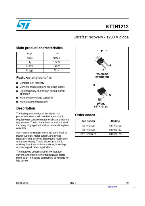
March 2006 Rev 11/99STTH1212Ultrafast recovery - 1200 V diodeMain product characteristicsFeatures and benefits■Ultrafast, soft recovery■Very low conduction and switching losses ■High frequency and/or high pulsed current operation■High reverse voltage capability ■High junction temperatureDescriptionThe high quality design of this diode has produced a device with low leakage current,regularly reproducible characteristics and intrinsic ruggedness. These characteristics make it ideal for heavy duty applications that demand long term reliability.Such demanding applications include industrial power supplies, motor control, and similarmission-critical systems that require rectification and freewheeling. These diodes also fit into auxiliary functions such as snubber, bootstrap, and demagnetization applications.The improved performance in low leakage current, and therefore thermal runaway guard band, is an immediate competitive advantage for this device.Order codesI F(AV)12 A V RRM 1200 V T j 175° C V F (typ) 1.25 V t rr (typ)50 nsPart Number Marking STTH1212D STTH1212D STTH1212G STTH1212G STTH1212G-TRSTTH1212GCharacteristics STTH12122/91 CharacteristicsTo evaluate the conduction losses use the following equation: P = 1.5 x I F(AV) + 0.033 I F 2(RMS)Table 1.Absolute ratings (limiting values at 25° C, unless otherwise specified)Symbol ParameterValue Unit V RRM Repetitive peak reverse voltage 1200V I F(RMS)RMS forward current30A I F(AV)Average forward current, δ = 0.5T c = 130° C12A I FRM Repetitive peak forward current t p = 5 µs, F = 5 kHz square 160A I FSM Surge non repetitive forward current t p = 10 ms Sinusoidal100A T stg Storage temperature range-65 to + 175°C T jMaximum operating junction temperature175°CTable 2.Thermal parameterSymbol ParameterValue Unit R th(j-c)Junction to case1.6°C/WTable 3.Static electrical characteristicsSymbol ParameterTest conditionsMin.TypMax.Unit I R (1)Reverse leakage currentT j = 25° C V R = V RRM10µAT j = 125° C 770V F (2)Forward voltage dropT j = 25° CI F = 12 A2.2V T j = 125° C 1.30 2.0T j = 150° C1.251.91.Pulse test: t p = 5 ms, δ < 2 %2.Pulse test: t p = 380 µs, δ < 2 %STTH1212Characteristics3/9Table 4.Dynamic characteristicsSymbolParameterTest conditionsMin.TypMax.Unitt rrReverse recovery timeI F = 1 A, dI F /dt = -50 A/µs, V R = 30 V , T j = 25° C 100nsI F = 1 A, dI F /dt = -100 A/µs,V R = 30 V , T j = 25° C 5070I RM Reverse recovery current I F = 12 A, dI F /dt = -200 A/µs,V R = 600 V , T j = 125° C 1624A S Softness factor I F = 12 A, dI F /dt = -200 A/µs,V R = 600 V , T j = 125° C 2t fr Forward recovery time I F = 12 A dI F /dt = 50 A/µs V FR = 1.5 x V Fmax , T j = 25° C 400ns V FPForward recovery voltageI F = 12 A, dI F /dt = 50 A/µs,T j = 25° C6VFigure 1.Conduction losses versusFigure 2.Forward voltage drop versusCharacteristicsSTTH12124/9Figure 3.Relative variation of thermal impedance junction to caseFigure 4.Peak reverse recovery current versus dI F /dt (typical values)Figure 5.Reverse recovery time versusFigure 6.Reverse recovery charges versusFigure 7.Softness factor versus dI F /dt (typical values)Figure 8.Relative variations of dynamic parameters versus junctionSTTH1212Characteristics5/9Figure 9.Transient peak forward voltageFigure 10.Forward recovery time versus dI F /dtFigure 11.Junction capacitance versusreverse voltage applied (typical values)Figure 12.Thermal resistance junction toambient versus copper surface under tab (Epoxy printed circuitPackage mechanical data STTH1212 2 Package mechanical dataEpoxy meets UL94, V0Cooling method: by conduction (C)Recommended torque value: 0.55 Nm (TO-220AC)Maximum torque value: 0.7 Nm (TO-220AC)6/9STTH1212Package mechanical data22In order to meet environmental requirements, ST offers these devices in ECOP ACK®packages. These packages have a Lead-free second level interconnect . The category ofsecond level interconnect is marked on the package and on the inner box label, incompliance with JEDEC Standard JESD97. The maximum ratings related to solderingconditions are also marked on the inner box label. ECOP ACK is an ST trademark.ECOP ACK specifications are available at: .7/9Ordering information STTH12128/93 Ordering information4 Revision historyPart Number Marking Package Weight Base qtyDelivery modeSTTH1212D STTH1212D TO-220AC 1.86 g 50Tube STTH1212G STTH1212G D 2P AK 1.48 g 50Tube STTH1212G-TRSTTH1212GD 2P AK1.48 g1000Tape & reelDate RevisionDescription of Changes02-Mar-20061First issue.STTH1212Please Read Carefully:Information in this document is provided solely in connection with ST products. STMicroelectronics NV and its subsidiaries (“ST”) reserve the right to make changes, corrections, modifications or improvements, to this document, and the products and services described herein at anytime, without notice.All ST products are sold pursuant to ST’s terms and conditions of sale.Purchasers are solely responsible for the choice, selection and use of the ST products and services described herein, and ST assumes no liability whatsoever relating to the choice, selection or use of the ST products and services described herein.No license, express or implied, by estoppel or otherwise, to any intellectual property rights is granted under this document. If any part of this document refers to any third party products or services it shall not be deemed a license grant by ST for the use of such third party products or services, or any intellectual property contained therein or considered as a warranty covering the use in any manner whatsoever of such third party products or services or any intellectual property contained therein.UNLESS OTHERWISE SET FORTH IN ST’S TERMS AND CONDITIONS OF SALE ST DISCLAIMS ANY EXPRESS OR IMPLIED WARRANTY WITH RESPECT TO THE USE AND/OR SALE OF ST PRODUCTS INCLUDING WITHOUT LIMITATION IMPLIED WARRANTIES OF MERCHANTABILITY, FITNESS FOR A PARTICULAR PURPOSE (AND THEIR EQUIVALENTS UNDER THE LAWS OF ANY JURISDICTION), OR INFRINGEMENT OF ANY PATENT, COPYRIGHT OR OTHER INTELLECTUAL PROPERTY RIGHT. UNLESS EXPRESSLY APPROVED IN WRITING BY AN AUTHORIZE REPRESENTATIVE OF ST, ST PRODUCTS ARE NOT DESIGNED, AUTHORIZED OR WARRANTED FOR USE IN MILITARY, AIR CRAFT, SPACE, LIFE SAVING, OR LIFE SUSTAINING APPLICATIONS, NOR IN PRODUCTS OR SYSTEMS, WHERE FAILURE OR MALFUNCTION MAY RESULT IN PERSONAL INJURY, DEATH, ORSEVERE PROPERTY OR ENVIRONMENTAL DAMAGE.Resale of ST products with provisions different from the statements and/or technical features set forth in this document shall immediately void any warranty granted by ST for the ST product or service described herein and shall not create or extend in any manner whatsoever, anyliability of ST.ST and the ST logo are trademarks or registered trademarks of ST in various countries.Information in this document supersedes and replaces all information previously supplied.The ST logo is a registered trademark of STMicroelectronics. All other names are the property of their respective owners.© 2006 STMicroelectronics - All rights reservedSTMicroelectronics group of companiesAustralia - Belgium - Brazil - Canada - China - Czech Republic - Finland - France - Germany - Hong Kong - India - Israel - Italy - Japan - Malaysia - Malta - Morocco - Singapore - Spain - Sweden - Switzerland - United Kingdom - United States of America9/9。
nRF24L01P产品说明书V1.0资料
nRF24L01+单片机2.4 GHz收发器产品说明书v1.0主要功能:全球通用的2.4 GHz ISM波段操作250kbps, 1Mbps and 2Mbps空中数据传输速率超低功率运行发射功率为0dBm(1.0mW)时,发射电流为11.3mA2Mbps空中数据传输速率,接收电流为13.5mA掉电电流为900nA待机-I电流26μA片内电压调整器1.9至3.6V电源供电范围增强型ShockBurst TM自动数据包处理自动包数据包事务处理6数据通道的MultiCeiver TM与nRF24L01嵌入式兼容空中数据速率250kbps 和1Mbps,与nRF2401A,nRF2402, nRF24E1和nRF24E2兼容低BOM成本±60ppm 16MHz晶振容许5V输入紧凑的20引脚4x4mm QFN封装应用无线 PC外围设备鼠标,键盘和遥控器三和一桌面捆绑先进的媒体中心遥控器网络电话耳机游戏控制器蓝牙模块运动手表和传感器消费电子产品射频遥控器家庭和商业自动化超低功率无线传感器网络RFID 射频识别资产跟踪系统玩具免责条款北欧半导体ASA有权做出随时更改,提高产品可靠性、功能或设计,不另行通知。
北欧半导体ASA不承担由于应用程序或使用任何所述产品或电路引起的责任。
所有应用程序的信息咨询,不构成说明书的组成部分。
极限值超过一个或多个限制的应力可能会造成设备永久性损坏。
这些应力等级只有在这样或那样的操作环境中提出,在规范中没有给出。
长时间暴露在限制值附近可能会影响设备的可靠性。
生命支持应用这些产品并非为因故障会引起人身伤害的维生装备,设备或系统设计的。
北欧半导体ASA客户使用或出售这些产品,他们将自担风险并同意完全赔偿北欧半导体ASA因使用不当或销售行为造成任何损害。
详细联系方式访问www.nordicsemi.no进入北欧半导体销售办事处和全世界的分销商网站总办公室:Otto Nielsens vei 127004 Trondheim电话: +47 72 89 89 00传真: +47 72 89 89 89www.nordicsemi.no写作惯例本产品规范遵循一套排版规则,文档一致,容易阅读。
FR24中文资料
25 50 75 100 125 150 175 ° Ambient Temperature (°C)
100 10 Number of Cycles @ 60 Hz
Typical Instantaneous Forward Characteristics 100 Forward Current (A)
FR20 . . . 210 Series Maximum Ratings Peak Repetitive Reverse Voltage...VRRM RMS Reverse Voltage...VR(rms) DC Blocking Voltage...VDC Average Forward Rectified Current...IF(av) TA = 55°C Non-Repetitive Peak Forward Surge Current...IFSM @ Rated Current & Temp Operating & Storage Temperature Range...TJ, TSTRG Electrical Characteristics Maximum Forward Voltage @ 2.0A...VF Maximum DC Reverse Current...IR @ Rated DC Blocking Voltage @ @ 25°C 100°C ............................................. 1.3 ............................................... FR20 50 35 50 FR21 100 70 100 FR22 200 140 200 FR24 400 280 400 FR26 600 420 600 FR28 800 560 800 FR210 1000 700 1000
UC3724中文资料
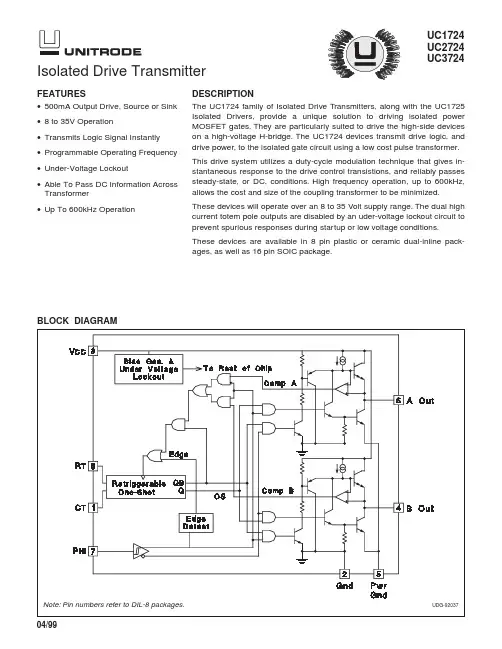
UC2724 UC3724FEATURES•500mA Output Drive, Source or Sink •8 to 35V Operation•Transmits Logic Signal Instantly •Programmable Operating Frequency •Under-Voltage Lockout•Able To Pass DC Information Across Transformer•Up To 600kHz Operation DESCRIPTIONThe UC1724family of Isolated Drive Transmitters,along with the UC1725 Isolated Drivers,provide a unique solution to driving isolated power MOSFET gates.They are particularly suited to drive the high-side devices on a high-voltage H-bridge.The UC1724devices transmit drive logic,and drive power, to the isolated gate circuit using a low cost pulse transformer.This drive system utilizes a duty-cycle modulation technique that gives in-stantaneous response to the drive control transistions,and reliably passes steady-state,or DC,conditions.High frequency operation,up to600kHz, allows the cost and size of the coupling transformer to be minimized.These devices will operate over an8to35Volt supply range.The dual high current totem pole outputs are disabled by an uder-voltage lockout circuit to prevent spurious responses during startup or low voltage conditions.These devices are available in8pin plastic or ceramic dual-inline pack-ages, as well as 16 pin SOIC package.Isolated Drive TransmitterBLOCK DIAGRAMUDG-92037 Note:Pin numbers refer to DIL-8 packages.CONNECTION DIAGRAMSELECTRICAL CHARACTERISTICS:Unless otherwise stated, V CC = 20V, R T = 4.3k Ω, C T = 1000pF, no load on anyoutput and these specifications apply for: –55o C < T A < 125o C for the UC1724, –25o C < T A < 85o C for the UC2724, and 0o C < T A < 70o C for the UC3724. T A =T J .PARAMETERTEST CONDITIONSMINTYPMAX UNITS Under-Voltage Lockout Start-Up Threshold V IN Rising7.759.5V Threshold Hysteresis 0.41.01.5V Retriggerable One-Shot Initial Accuracy T J = 25°C 1.54 1.92.25µs Temperature Stability Over Operating T J 1.02.9µs Voltage Stability V IN = 10 to 35V 0.20.5%/V Operating Frequency L LOAD = 1.4mH 100150200kHz Minimum Pulse Width RT = 2k CT = 300pF1005001200ns Operating FrequencyRT = 2k C T = 300pF L LOAD = 1.4mH5007501100kHzABSOLUTE MAXIMUM RATINGSSupply Voltage V IN . . . . . . . . . . . . . . . . . . . . . . . . . . . . . . .40V Source/Sink Current (Pulsed). . . . . . . . . . . . . . . . . . . . . . . .1A Source/Sink Current (Continuous). . . . . . . . . . . . . . . . . . .0.5A Ouput Voltage (Pins 4, 6). . . . . . . . . . . . . . .–0.3 to (V IN +0.3)V P HI , R T , and C T inputs (Pins 1, 7, and 8). . . . . . . . .–0.3 to 6V Operating Junction Temperature (Note 2). . . . . . . . . . . .150°C Storage Temperature Range . . . . . . . . . . . . . .–65°C to 150°C Lead Temperature (Soldering, 10 Seconds). . . . . . . . . .300°C Note 1:All voltages are with respect to GND (Pin 2);all cur-rents are positive into, negative out of part.Note 2:Consult Unitrode Integrated Circuit Databook for ther-mal limitations and considerations of package.Note 3:Pin numbers refer to DIL-8 packages.RECOMMENDED OPERATION CONDITIONSInput Voltage . . . . . . . . . . . . . . . . . . . . . . . . . . . . .+9V to +35V Sink/Source Load Current (each output). . . . . . . . .0 to 500mA Timing Resistor. . . . . . . . . . . . . . . . . . . . . . . . . . .2kW to 10kW Timing Capacitor . . . . . . . . . . . . . . . . . . . . . . . . .300pF to 3nF Operating Temperature Range (UC1724). . .–55°C<T A <125°C Operating Temperature Range (UC3724). . . . . .0°C<T A <70°C Note 4:Range over which the device is functional andparameter limits are guaranteed.TEMPERATURE RANGE PACKAGE UC1724J –55°C to +125°C CDIPUC2724DW –25°C to +85°C SOIC-Wide UC2724N PDIPUC3724DW 0°C to +70°CSOIC-Wide UC3724NPDIPORDERING INFORMATIONELECTRICAL CHARACTERISTICS:Unless otherwise stated, V CC = 20V, R T = 4.3k Ω, C T = 1000pF, no load on anyoutput and these specifications apply for: –55o C < T A < 125o C for the UC1724, –25o C < T A < 85o C for the UC2724, and 0o C < T A < 70o C for the UC3724. T A =T J .PARAMETERTEST CONDITIONSMINTYPMAX UNITSPhi Input (Control Input)HIGH Input Voltage 2.0V LOW Input Voltage 0.8V HIGH Input Current V IH =+2.4V –220–130µA LOW Input Current V IL =+0.4V–600–300µA Delay to One-Shot 350ns Delay to Output 250nsOutput Drivers Output Low LevelI SINK = 50mA 0.30.4V I SINK = 250mA 0.5 2.1V Output High Level (Volts Below V CC )I SOURCE = 50 mA 1.5 2.1V I SOURCE = 250 mA 1.7 2.5V Rise/Fall Time No load3090nsTotal Supply Current Supply CurrentC T = 1.4V1530mAUNITRODE CORPORA TION7 CONTINENTAL BLVD.• MERRIMACK, NH 03054TEL.(603) 424-2410FAX (603) 424-3460Additional InformationPlease refer to the following Unitrode application topics.[1]Application Note U-127,Unique Chip Pair Simplified Isolated High-Side Switch Drive by John A.O’Connor.[2]Design Note DN-35,IGBT Drive Using MOSFET Gate Drivers by John A.O’Conner.IMPORTANT NOTICETexas Instruments and its subsidiaries (TI) reserve the right to make changes to their products or to discontinue any product or service without notice, and advise customers to obtain the latest version of relevant information to verify, before placing orders, that information being relied on is current and complete. All products are sold subject to the terms and conditions of sale supplied at the time of order acknowledgement, including those pertaining to warranty, patent infringement, and limitation of liability.TI warrants performance of its semiconductor products to the specifications applicable at the time of sale in accordance with TI’s standard warranty. Testing and other quality control techniques are utilized to the extent TI deems necessary to support this warranty. Specific testing of all parameters of each device is not necessarily performed, except those mandated by government requirements.CERTAIN APPLICATIONS USING SEMICONDUCTOR PRODUCTS MAY INVOLVE POTENTIAL RISKS OF DEATH, PERSONAL INJURY, OR SEVERE PROPERTY OR ENVIRONMENTAL DAMAGE (“CRITICAL APPLICATIONS”). TI SEMICONDUCTOR PRODUCTS ARE NOT DESIGNED, AUTHORIZED, OR WARRANTED TO BE SUITABLE FOR USE IN LIFE-SUPPORT DEVICES OR SYSTEMS OR OTHER CRITICAL APPLICATIONS. INCLUSION OF TI PRODUCTS IN SUCH APPLICATIONS IS UNDERSTOOD TO BE FULLY AT THE CUSTOMER’S RISK.In order to minimize risks associated with the customer’s applications, adequate design and operating safeguards must be provided by the customer to minimize inherent or procedural hazards.TI assumes no liability for applications assistance or customer product design. TI does not warrant or represent that any license, either express or implied, is granted under any patent right, copyright, mask work right, or other intellectual property right of TI covering or relating to any combination, machine, or process in which such semiconductor products or services might be or are used. TI’s publication of information regarding any third party’s products or services does not constitute TI’s approval, warranty or endorsement thereof.Copyright © 1999, Texas Instruments Incorporated。
AM42DL1624DT35IT资料
Publication# 25790 Rev: A Amendment/0 Issue Date: January 9, 2002
Refer to AMD’s Website () for the latest information.
元器件交易网
s Top or bottom boot block s Manufactured on 0.23 µm process technology s Compatible with JEDEC standards
— Pinout and software compatible with single-power-supply flash standard
s Package
— 69-Ball FBGA
s Supports Common Flash Memory Interface (CFI) s Erase Suspend/Erase Resume
— Suspends erase operations to allow programming in same bank
s Power supply voltage of 2.7 to 3.3 volt s High performance
— Access time as fast as 70 ns
SOFTWARE FEATURES
s Data Management Software (DMS)
— AMD-supplied software manages data programming and erasing, enabling EEPБайду номын сангаасOM emulation — Eases sector erase limitations
AiP1624中文使用手册
忽略。
4 逻辑电源
VDD
电源电压
5 输出(段)
SEG1
段输出,P 管开漏输出。
6 输出(段)
SEG2
段输出,P 管开漏输出。
7 输出(段)
SEG3
段输出,P 管开漏输出。
8 输出(段)
SEG4
段输出,P 管开漏输出。
9 输出(段)
SEG5
段输出,P 管开漏输出。
10 输出(段)
SEG6
段输出,P 管开漏输出。
GRID4
08HL
08HU
09HL
09HU
GRID5
0AHL
0AHU
0BHL
0BHU
GRID6
0CHL
0CHU
0DHL
0DHU
GRID7
江苏省无锡市蠡园经济开发区滴翠路 100 号 9 栋 2 层
http://www.i-core. cn
邮编:214072
第 5 页 共 12 页 版本:2012-01-B1
数据写模式设定 00:写数据到显示寄存器
地址增加模式设定(对于显示寄存): 0:写一字节数据后地址增加 1:固定地址
江苏省无锡市蠡园经济开发区滴翠路 100 号 9 栋 2 层
http://www.i-core. cn
邮编:214072
第 6 页 共 12 页 版本:2012-01-B1
表 733-11-I
MSB
LSB
0 0 - - - - b1 b0
不考虑
上电时,设置模式为 7 位,11 段。
00 4 位,14 段 01 5 位,13 段 10 6 位,12 段 11 7 位,11 段
(2)数据设置 该指令用来设置数据写
LCD12864液晶显示器中文说明
L C D12864液晶显示器中文说明(共16页)--本页仅作为文档封面,使用时请直接删除即可----内页可以根据需求调整合适字体及大小--一、液晶显示模块概述12864A-1汉字图形点阵液晶显示模块,可显示汉字及图形,内置8192个中文汉字(16X16点阵)、128个字符(8X16点阵)及64X256点阵显示RAM(GDRAM)。
主要技术参数和显示特性:电源:VDD ~+5V(内置升压电路,无需负压);显示内容:128列× 64行显示颜色:黄绿显示角度:6:00钟直视LCD类型:STN与MCU接口:8位或4位并行/3位串行配置LED背光多种软件功能:光标显示、画面移位、自定义字符、睡眠模式等二、外形尺寸1.外形尺寸图2.主要外形尺寸项目标准尺寸单位模块体积××mm定位尺寸×mm视域×mm行列点阵数128×64dots点距离×mm点大小×mm二、模块引脚说明128X64 引脚说明引脚号引脚名称方向功能说明1VSS-模块的电源地2VDD-模块的电源正端3V0-LCD驱动电压输入端4RS(CS)H/L并行的指令/数据选择信号;串行的片选信号5R/W(SID)H/L并行的读写选择信号;串行的数据口6E(CLK)H/L并行的使能信号;串行的同步时钟7DB0H/L数据08DB1H/L数据19DB2H/L数据210DB3H/L数据311DB4H/L数据412DB5H/L数据513DB6H/L数据614DB7H/L数据715PSB H/L并/串行接口选择:H-并行;L-串行16NC空脚17/RET H/L复位低电平有效18NC空脚19LED_A-背光源正极(LED+5V)20LED_K-背光源负极(LED-OV)逻辑工作电压(VDD):~电源地(GND):0V工作温度(Ta):0~60℃(常温) / -20~75℃(宽温)三、接口时序模块有并行和串行两种连接方法(时序如下):8位并行连接时序图MPU写资料到模块MPU从模块读出资料2、串行连接时序图串行数据传送共分三个字节完成:第一字节:串口控制—格式 11111ABCA为数据传送方向控制:H表示数据从LCD到MCU,L表示数据从MCU到LCD B为数据类型选择:H表示数据是显示数据,L表示数据是控制指令C固定为0第二字节:(并行)8位数据的高4位—格式 DDDD0000第三字节:(并行)8位数据的低4位—格式 0000DDDD串行接口时序参数:(测试条件:T=25℃ VDD=四、用户指令集1、指令表1:(RE=0:基本指令集)指令指令码说明执行时间(540KHZ)RSRWDB7DB6DB5DB4DB3DB2DB1DB清除显示0000000001将DDRAM填满“20H”,并且设定DDRAM的地址计数器(AC)到“00H”地址归位000000001X设定DDRAM的地址计数器(AC)到“00H”,并且将游标移到开头原点位置;这个指令并不改变DDRAM的内容进入点设定00000001I/D S指定在资料的读取与写入时,设定游标移动方向及指定显示的移位72us显示状态开/关0000001D C BD=1:整体显示ONC=1:游标ONB=1:游标位置ON72us游标或显示移位控制000001S/CR/LX X设定游标的移动与显示的移位控制位元;这个指令并不改变DDRAM的内容72us备注:1、当模块在接受指令前,微处理顺必须先确认模块内部处于非忙碌状态,即读取BF 标志时BF 需为0,方可接受新的指令;如果在送出一个指令前并不检查BF 标志,那么在前一个指令和这个指令中间必须延迟一段较长的时间,即是等待前一个指令确实执行完成,指令执行的时间请参考指令表中的个别指令说明。
ATX FNES LED系列自包容紧急照明设备说明书
• EURASEC N° TC RU C-FR.ГБ05.B.00912
Other Certification
• INMETRO Certificate: BVC11.0815
Related Products
• For labels see Labels for Emergency Lighting Units, ATX SelfAdhesive Signaling Labels for Emergency Lighting Units.
ATX™ FNES LED Series Self-Contained Emergency Lighting
Zone 2 - 21 and 22. With Self-Test System
ATEX/IECEx: Zone 2 - 21 and 22 II 2 D and II 3 GD IP66/67 - IK10
FNES LED
— Optional increased control system capacity: booster (repeater unit) is used to increase the length of the network allowing up to 1000 emergency lighting units to be on one control system. This allows for the use of a single computer to centralize the management of the facilities emergency lighting system. For more information, please contact your local sales representative.
74ALVTH16244VRG4,74ALVTH16244DLRG4,74ALVTH16244ZQLR,74ALVTH16244DLG4, 规格书,Datasheet 资料
PACKAGE OPTION ADDENDUM20-Aug-2011Addendum-Page 1PACKAGING INFORMATIONOrderable Device Status(1)Package Type PackageDrawingPins Package QtyEco Plan(2)Lead/Ball FinishMSL Peak Temp(3)Samples (Requires Login)74ALVTH16244DLG4ACTIVE SSOP DL 4825Green (RoHS & no Sb/Br)CU NIPDAU Level-1-260C-UNLIM 74ALVTH16244DLRG4ACTIVE SSOP DL 481000Green (RoHS & no Sb/Br)CU NIPDAU Level-1-260C-UNLIM 74ALVTH16244GRE4ACTIVE TSSOP DGG 482000Green (RoHS & no Sb/Br)CU NIPDAU Level-1-260C-UNLIM 74ALVTH16244GRG4ACTIVE TSSOP DGG 482000Green (RoHS & no Sb/Br)CU NIPDAU Level-1-260C-UNLIM 74ALVTH16244VRE4ACTIVE TVSOP DGV 482000Green (RoHS & no Sb/Br)CU NIPDAU Level-1-260C-UNLIM 74ALVTH16244VRG4ACTIVE TVSOP DGV 482000Green (RoHS & no Sb/Br)CU NIPDAU Level-1-260C-UNLIM 74ALVTH16244ZQLRACTIVEBGA MICROSTAR JUNIORZQL561000Green (RoHS & no Sb/Br)SNAGCULevel-1-260C-UNLIMSN74ALVTH16244DL ACTIVE SSOP DL 4825Green (RoHS & no Sb/Br)CU NIPDAU Level-1-260C-UNLIM SN74ALVTH16244DLR ACTIVE SSOP DL 481000Green (RoHS & no Sb/Br)CU NIPDAU Level-1-260C-UNLIM SN74ALVTH16244GR ACTIVE TSSOP DGG 482000Green (RoHS & no Sb/Br)CU NIPDAU Level-1-260C-UNLIM SN74ALVTH16244VRACTIVETVSOPDGV482000Green (RoHS & no Sb/Br)CU NIPDAU Level-1-260C-UNLIM(1)The marketing status values are defined as follows:ACTIVE: Product device recommended for new designs.LIFEBUY: TI has announced that the device will be discontinued, and a lifetime-buy period is in effect.NRND: Not recommended for new designs. Device is in production to support existing customers, but TI does not recommend using this part in a new design.PREVIEW: Device has been announced but is not in production. Samples may or may not be available.OBSOLETE: TI has discontinued the production of the device.(2)Eco Plan - The planned eco-friendly classification: Pb-Free (RoHS), Pb-Free (RoHS Exempt), or Green (RoHS & no Sb/Br) - please check /productcontent for the latest availability information and additional product content details.TBD: The Pb-Free/Green conversion plan has not been defined.Pb-Free (RoHS): TI's terms "Lead-Free" or "Pb-Free" mean semiconductor products that are compatible with the current RoHS requirements for all 6 substances, including the requirement that lead not exceed 0.1% by weight in homogeneous materials. Where designed to be soldered at high temperatures, TI Pb-Free products are suitable for use in specified lead-free processes.芯天下--/PACKAGE OPTION ADDENDUM20-Aug-2011Addendum-Page 2Pb-Free (RoHS Exempt): This component has a RoHS exemption for either 1) lead-based flip-chip solder bumps used between the die and package, or 2) lead-based die adhesive used between the die and leadframe. The component is otherwise considered Pb-Free (RoHS compatible) as defined above.Green (RoHS & no Sb/Br): TI defines "Green" to mean Pb-Free (RoHS compatible), and free of Bromine (Br) and Antimony (Sb) based flame retardants (Br or Sb do not exceed 0.1% by weight in homogeneous material)(3)MSL, Peak Temp. -- The Moisture Sensitivity Level rating according to the JEDEC industry standard classifications, and peak solder temperature.Important Information and Disclaimer:The information provided on this page represents TI's knowledge and belief as of the date that it is provided. TI bases its knowledge and belief on information provided by third parties, and makes no representation or warranty as to the accuracy of such information. Efforts are underway to better integrate information from third parties. TI has taken and continues to take reasonable steps to provide representative and accurate information but may not have conducted destructive testing or chemical analysis on incoming materials and chemicals.TI and TI suppliers consider certain information to be proprietary, and thus CAS numbers and other limited information may not be available for release.In no event shall TI's liability arising out of such information exceed the total purchase price of the TI part(s) at issue in this document sold by TI to Customer on an annual basis.芯天下--/TAPE AND REELINFORMATION*Alldimensions are nominalDevicePackage Type Package Drawing Pins SPQReel Diameter (mm)Reel Width W1(mm)A0(mm)B0(mm)K0(mm)P1(mm)W (mm)Pin1Quadrant 74ALVTH16244ZQLR BGA MI CROSTA R JUNI OR ZQL561000330.016.44.87.31.58.016.0Q1SN74ALVTH16244DLR SSOP DL 481000330.032.411.3516.2 3.116.032.0Q1SN74ALVTH16244GR TSSOP DGG 482000330.024.48.615.8 1.812.024.0Q1SN74ALVTH16244VRTVSOPDGV482000330.016.47.110.21.612.016.0Q114-Jul-2012*Alldimensions are nominalDevicePackage Type Package DrawingPins SPQ Length (mm)Width (mm)Height (mm)74ALVTH16244ZQLR BGA MICROSTARJUNIORZQL 561000333.2345.928.6SN74ALVTH16244DLR SSOP DL 481000367.0367.055.0SN74ALVTH16244GR TSSOP DGG 482000367.0367.045.0SN74ALVTH16244VRTVSOPDGV482000367.0367.038.014-Jul-2012IMPORTANT NOTICETexas Instruments Incorporated and its subsidiaries(TI)reserve the right to make corrections,enhancements,improvements and other changes to its semiconductor products and services per JESD46C and to discontinue any product or service per JESD48B.Buyers should obtain the latest relevant information before placing orders and should verify that such information is current and complete.All semiconductor products(also referred to herein as“components”)are sold subject to TI’s terms and conditions of sale supplied at the time of order acknowledgment.TI warrants performance of its components to the specifications applicable at the time of sale,in accordance with the warranty in TI’s terms and conditions of sale of semiconductor products.Testing and other quality control techniques are used to the extent TI deems necessary to support this warranty.Except where mandated by applicable law,testing of all parameters of each component is not necessarily performed.TI assumes no liability for applications assistance or the design of Buyers’products.Buyers are responsible for their products and applications using TI components.To minimize the risks associated with Buyers’products and applications,Buyers should provide adequate design and operating safeguards.TI does not warrant or represent that any license,either express or implied,is granted under any patent right,copyright,mask work right,or other intellectual property right relating to any combination,machine,or process in which TI components or services are rmation published by TI regarding third-party products or services does not constitute a license to use such products or services or a warranty or endorsement e of such information may require a license from a third party under the patents or other intellectual property of the third party,or a license from TI under the patents or other intellectual property of TI.Reproduction of significant portions of TI information in TI data books or data sheets is permissible only if reproduction is without alteration and is accompanied by all associated warranties,conditions,limitations,and notices.TI is not responsible or liable for such altered rmation of third parties may be subject to additional restrictions.Resale of TI components or services with statements different from or beyond the parameters stated by TI for that component or service voids all express and any implied warranties for the associated TI component or service and is an unfair and deceptive business practice. TI is not responsible or liable for any such statements.Buyer acknowledges and agrees that it is solely responsible for compliance with all legal,regulatory and safety-related requirements concerning its products,and any use of TI components in its applications,notwithstanding any applications-related information or support that may be provided by TI.Buyer represents and agrees that it has all the necessary expertise to create and implement safeguards which anticipate dangerous consequences of failures,monitor failures and their consequences,lessen the likelihood of failures that might cause harm and take appropriate remedial actions.Buyer will fully indemnify TI and its representatives against any damages arising out of the use of any TI components in safety-critical applications.In some cases,TI components may be promoted specifically to facilitate safety-related applications.With such components,TI’s goal is to help enable customers to design and create their own end-product solutions that meet applicable functional safety standards and requirements.Nonetheless,such components are subject to these terms.No TI components are authorized for use in FDA Class III(or similar life-critical medical equipment)unless authorized officers of the parties have executed a special agreement specifically governing such use.Only those TI components which TI has specifically designated as military grade or“enhanced plastic”are designed and intended for use in military/aerospace applications or environments.Buyer acknowledges and agrees that any military or aerospace use of TI components which have not been so designated is solely at the Buyer's risk,and that Buyer is solely responsible for compliance with all legal and regulatory requirements in connection with such use.TI has specifically designated certain components which meet ISO/TS16949requirements,mainly for automotive ponents which have not been so designated are neither designed nor intended for automotive use;and TI will not be responsible for any failure of such components to meet such requirements.Products ApplicationsAudio /audio Automotive and Transportation /automotiveAmplifiers Communications and Telecom /communicationsData Converters Computers and Peripherals /computersDLP®Products Consumer Electronics /consumer-appsDSP Energy and Lighting /energyClocks and Timers /clocks Industrial /industrialInterface Medical /medicalLogic Security /securityPower Mgmt Space,Avionics and Defense /space-avionics-defense Microcontrollers Video and Imaging /videoRFID OMAP Mobile Processors /omap TI E2E Community Wireless Connectivity /wirelessconnectivityMailing Address:Texas Instruments,Post Office Box655303,Dallas,Texas75265Copyright©2012,Texas Instruments Incorporated。
- 1、下载文档前请自行甄别文档内容的完整性,平台不提供额外的编辑、内容补充、找答案等附加服务。
- 2、"仅部分预览"的文档,不可在线预览部分如存在完整性等问题,可反馈申请退款(可完整预览的文档不适用该条件!)。
- 3、如文档侵犯您的权益,请联系客服反馈,我们会尽快为您处理(人工客服工作时间:9:00-18:30)。
PACIFIC DISPLAY DEVICESLCD Component Data SheetModel Number: 1624416 Character by 2 LineAlphanumeric LCD AssemblyWith Embedded ControllerCONTENTSINFORMATION1. GENERALProductOverview 2 1.11.2 Part Numbering System 2Ratings 3 Maximum1.3Absolute1.4 Circuit Block Diagram 3Characteristics 3 Mechanical1.51.6 Input Signal Function 41.7 LCM Contrast Control and Bias 4Dimensions 5 LCD1.82. ELECTRICAL / OPTICAL CHARACTERISTICS2.1 DC Electrical Characteristics 62.2 AC Electrical Characteristics 6Characteristics 8 2.3Optical2.4 LED Backlight Characteristics 92.5 EL Panel Backlight Characteristics 93. OPERATING PRINCIPALS AND METHODS3.1 LCD Controller Display and Control Functions 103.2 Display Data RAM Address Map 124. RELIABILITY 135. PRECAUTIONS FOR USING LCD MODULES 14139 Avenida Victoria – Suite 100 – San Clemente, CA – 92672SPECIFICATIONS FOR LIQUID CRYSTAL DISPLAY MODULE MODEL NO: 16244 1. GENERAL INFORMATION1.1 Product Overview•16 Character x 2 line Alphanumeric Dot Matrix LCD Module•LCD Controller: Embedded S6A0069 or equivalent alpha-numeric controller•Multiplexing driving: 1/16 duty, 1/5 bias•Operating Mode: Super Twisted Nematic (STN) technology•LCD Module Service Life: 100,000 hours minimum1.2 Part Numbering System16244-SL-F-ST-LED-GY-6¾• (Blank)¾•••¾•••¾••¾•••¾••••¾• (-6) 6 o’clock• (-12) 12 0’clockSPECIFICATIONS FOR LIQUID CRYSTAL DISPLAY MODULE MODEL NO: 162441.3 Absolute Maximum RatingsSupply voltage for logic V DD Supply voltage for LCD V DD – V0 -- V DD +0.3 V Input voltage VI -0.3 V DD +0.3V Standard Operating temperature TOP (-ST) 0 50 ºC Standard Storage temperature TST (-ST) -10 60 ºC Extended Operating temperature TOP (-ET) -20 70 ºC Extended Storage temperature TST (-ET) -30 80 ºC Soldering Temp Tsolder 260 ºC1.4 Circuit Block DiagramV OV DD E~1.5 Mechanical CharacteristicsItem Contents UnitModule size (W ×H ×T)84.0 x 44.0 x 14.2 Max (w/ LED Backlight) 84.0 x 44.0 x 10.0 Max (w/ ELP, Reflective) mm Viewing area (W ×H)62.2 x 17.9 mm Character matrix (W ×H) 5 × 8dots Character size (W ×H)2.95 x 5.55 mm Dot size (W ×H)0.55 x 0.65 mm Dot pitch (W ×H)0.60 x 0.70 mmSPECIFICATIONS FOR LIQUID CRYSTAL DISPLAY MODULE MODEL NO: 16244 1.6 Input Signal FunctionPin NO. Symbol Level Description1 VSS 0V Ground2 VDD 5.0V Supply voltage for logic3 VO --- Input voltage for LCD4 RS H/L H : Data signal, L : Instruction signal5 R/W H/L H : Read mode, L : Write modeH6 EH,→ L Chip enable signal7 DB0 H/L Data bit 08 DB1 H/L Data bit 19 DB2 H/L Data bit 210 DB3 H/L Data bit 311 DB4 H/L Data bit 412 DB5 H/L Data bit 513 DB6 H/L Data bit 614 DB7 H/L Data bit 715 LED A(+) 4.2V Back light anode16 LED K (-) 0V Back light cathode1.7 LCM Contrast Control and BiasSPECIFICATIONS FOR LIQUID CRYSTAL DISPLAY MODULE MODEL NO: 16244 1.8 LCM DimensionsSPECIFICATIONS FOR LIQUID CRYSTAL DISPLAY MODULE MODEL NO: 162442. ELECTRICAL / OPTICAL CHARACTERISTICS2.1 DC Electrical Characteristics (V DD = +5V±10% , V SS = 0V, Ta = 25°C )UnitMin Typ Max Parameter SymbolConditionV Supply voltage for logic V DD--- 4.5 5.0 5.5mA Supply current for logic I DD--- --- 1.38 30°C --- 5.10 --- V Operating voltage for LCD* V DD-V O25°C --- 4.50 --- V50°C --- 4.30 --- VV Input voltage ' H ' level V IH--- 2.2 --- VDDInput voltage ' L ' level V IL--- -0.3 --- 0.6 V *Note: -ET temp range will require up to maximun 8V biasing and require a minimum external voltage supply of -3V @-20°C.2.2 AC Electrical Characteristics•Write Modepin Characteristic SymbolMin. Typ. Max. Unit TestE cycle time t C500 --- --- ns EE rise time t r--- --- 25 ns EE fall time t f--- --- 25 ns EE pulse width (High, Low) t W220 --- --- ns ERS R/W and RS set-up time t SU140 --- --- ns R/W,RS R/W and RS hold time t h110 --- --- ns R/W,Data set-up time t SU260 --- --- ns DB0 ~ DB7Data hold time t h210 --- --- ns DB0 ~ DB7SPECIFICATIONS FOR LIQUID CRYSTAL DISPLAY MODULE MODEL NO: 16244 •Read ModeSPECIFICATIONS FOR LIQUID CRYSTAL DISPLAY MODULE MODEL NO: 162442.3 Optical Characteristics (V OP = 4.7V, Ta = 25°C )Item Symbol Condition Min Typ Max Unit Remarks NoteTr --- --- 250 380 ms --- 1Response timeTf --- --- 200 300 ms --- 1Contrast Ratio Cr --- 3 5.0 --- --- --- 2 Frame Frequency f F --- --- 64 --- Hz --- 225 --- --- deg ∅ = 90° 3 33 --- --- deg ∅ = 270°3 52 --- --- deg ∅ = 0°3 Viewing angle range θCr ≥ 2 33 --- --- deg ∅ = 180°3SPECIFICATIONS FOR LIQUID CRYSTAL DISPLAY MODULE MODEL NO: 162442.4 LED Backlight Characteristics■ Yellow-Green LED Operating Characteristics (5V - Array Lit)StandardItem Symbol Conditions Min. Typ. Max.UnitForward Voltage V f Ta= 25 °C 3.8 4.1 4.4 VDC Forward Current I F Ta= 25 °C --- 120 260 mA Reverse Voltage V R Ta= 25 °C --- 8 --- V■ Life (Array or Edge Lit)StandardItem Conditions Min. Max.UnitLife Ta= 25 °C 100,000 --- hrs2.5 EL Panel Backlight Characteristics■ Blue-Green EL Panel Operating Characteristics:StandardItem Conditions Min. Typ. Max.UnitCurrent Consumption 100VAC RMS, 400HzTa: 25°C--- 2.5 3.9 mAEL Drive Voltage --- --- 100 150 VAC RMS EL Drive Frequency --- --- 400 1000 Hz Operating Temperature --- -35°C --- +50°C °C Storage Temperature --- -40°C --- +60°C °CLuminance 40 50 --- cd/m 2Luminance Half-Life100VAC RMS, 400Hz Ta: 25°C 3500 --- --- Hrs *Note: half life is defined as Luminance being reduced by 50%SPECIFICATIONS FOR LIQUID CRYSTAL DISPLAY MODULE MODEL NO: 16244 3. OPERATING PRINCIPALS AND METHODESSPECIFICATIONS FOR LIQUID CRYSTAL DISPLAY MODULE MODEL NO: 16244 •Initializing by InstructionPower On|Wait for more than 15ms after VDD rises to 4.5V|RS R/W DB7 DB6 DB5 DB4 DB3 DB2 DB1 DB0 0 0 0 0 1 1 * * * * BF cannot be checked before this instruction. Function Set| Wait for more than 4.1ms|RS R/W DB7 DB6 DB5 DB4 DB3 DB2 DB1 DB0 0 0 0 0 1 1 * * * * BF cannot be checked before this instruction. Function Set| Wait for more than 100μs|RS R/W DB7 DB6 DB5 DB4 DB3 DB2 DB1 DB0 0 0 0 0 1 1 * * * * BF cannot be checked before this instruction. Function Set|| | | | BF can be checked after following instruction.When BF is not checked, the waiting time between instructions is longer than execution instruction time.|RS R/W DB7 DB6 DB5 DB4 DB3 DB2 DB1 DB0 0 0 0 0 1 1 N F * * Function Set (Specify the number of display lines and character font.) The number of display lines and character font cannot be changed afterwards.0 0 0 0 0 0 1 0 0 0 Display Off0 0 0 0 0 0 0 0 0 1 Display Clear 0 0 0 0 0 0 0 1 I/D S Entry Mode Set||ÈInitialization endsSPECIFICATIONS FOR LIQUID CRYSTAL DISPLAY MODULE MODEL NO: 16244 3.2 Display Data RAM Address MapLCD Character Location mapCharacters 1 2 3 4 5 6 7 8 9 1011 12 13 14 15 16 First line 00H 01H 02H 03H 04H05H06H07H08H09H0AH0BH 0CH 0DH 0EH0FH Second line 40H 41H 42H 43H 44H45H46H47H48H49H4AH4BH 4CH 4DH 4EH4FHSPECIFICATIONS FOR LIQUID CRYSTAL DISPLAY MODULE MODEL NO: 16244 4. RELIABILITYLCD Panel Service LifeDefinition of panel service life•100,000 hours minimum at 25° C ±10%•Contrast becomes 30% of initial value•Current consumption becomes three times higher than initial value•Remarkable alignment deterioration occurs in LCD cell layer•Unusual operation occurs in display functionsSPECIFICATIONS FOR LIQUID CRYSTAL DISPLAY MODULE MODEL NO: 16244 5. PRECAUTIONS FOR USING LCD MODULESInstalling LCD ModulesThe hole in the printed circuit board is used to fix LCM as shown in the picture below. Attend to the following items when installing the LCM.1)Cover the surface with a transparent protective plate to protect the polarizer and LC cell.2)When assembling the LCM into other equipment, the spacer to the bit between the LCM and the fitting plateshould have enough height to avoid causing stress to the module surface, refer to the individual specifications formeasurements. The measurement tolerance should be ±0.1mm.Precaution for Handing LCD ModulesSince LCM has been assembled and adjusted with a high degree of precision, avoid applying excessive shocks to the module or making any alterations or modifications to it.1)Cover the surface with a transparent protective plate to protect the polarizer and LC cell.2)Do not alter, modify or change the shape of the tab on the metal frame.3)Do not make extra holes on the printed circuit board, modify its shape or change the positions of components tobe attached.4)Do not damage or modify the pattern writing on the printed circuit board.5)Absolutely do not modify the zebra rubber strip (conductive rubber) or heat seal connector.6)Except for soldering the interface, do not make any alterations or modifications with a soldering iron.7)Do not drop, bend or twist LCM.Electro-Static Discharge ControlSince this module uses a CMOS LSI, the same careful attention should be paid to electrostatic discharge as for an ordinary CMOS IC.1)Make certain that you are grounded when handing LCM.2)Before remove LCM from its packing case or incorporating it into a set, be sure the module and your body havethe same electric potential.3)When soldering the terminal of LCM, make certain the AC power source for the soldering iron does not leak.4)When using an electric screwdriver to attach LCM, the screwdriver should be of ground potentiality to minimizeas much as possible any transmission of electromagnetic waves produced sparks coming from the commutator ofthe motor.5)As far as possible make the electric potential of your work clothes and that of the work bench the groundpotential.6)To reduce the generation of static electricity be careful that the air in the work is not too dried. A relativehumidity of 50%-60% is recommended.Precaution for soldering to the LCM1)Observe the following when soldering lead wire, connector cable and etc. to the LCM.a)Soldering iron temperature : 280°C ± 10°C.b)Soldering time : 3-4 sec.2)Solder : eutectic solder.SPECIFICATIONS FOR LIQUID CRYSTAL DISPLAY MODULE MODEL NO: 162443)If soldering flux is used, be sure to remove any remaining flux after finishing to soldering operation. (This doesnot apply in the case of a non-halogen type of flux.) It is recommended that you protect the LCD surface with acover during soldering to prevent any damage due to flux spatters.4)When soldering the electroluminescent panel and PC board, the panel and board should not be detached morethan three times. This maximum number is determined by the temperature and time conditions mentioned above,though there may be some variance depending on the temperature of the soldering iron.5)When remove the electroluminescent panel from the PC board, be sure the solder has completely melted, thesoldered pad on the PC board could be damaged.Precautions for Operation1)Viewing angle varies with the change of liquid crystal driving voltage (VO). Adjust VO to show the best contrast.2)Driving the LCD in the voltage above the limit shortens its life.3)Response time is greatly delayed at temperature below the operating temperature range. However, this does notmean the LCD will be out of the order. It will recover when it returns to the specified temperature range.4)If the display area is pushed hard during operation, the display will become abnormal. However, it will return tonormal if it is turned off and then back on.5)Condensation on terminals can cause an electrochemical reaction disrupting the terminal circuit. Therefore, itmust be used under the relative condition of 40°C , 50% RH.6)When turning the power on, input each signal after the positive/negative voltage becomes stable.Safety•If the LCD panel breaks, be careful not to get the liquid crystal in your mouth. If the liquid crystal touches your skin or clothes, wash it off immediately using soap and plenty of water.Handling•The display panel is made of glass. Do not subject it to a mechanical shock by dropping it or impact.•If the display panel is damaged and the liquid crystal substance leaks out, be sure not to get any in your mouth. If the substance contacts your skin or clothes, wash it off using soap and water.•Do not apply excessive force to the display surface or the adjoining areas since this may cause the color tone to vary.•The polarizer covering the display surface of the LCD module is soft and easily scratched. Handle this polarizer carefully.•If the display surface becomes contaminated, breathe on the surface and gently wipe it with a soft dry cloth. If it is heavily contaminated, moisten cloth with one of the following solvents :o Isopropyl alcoholo Ethyl alcohol•Solvents other than those above-mentioned may damage the polarizer. Especially, do not use the following.o Watero Ketoneo Aromatic solvents•Exercise care to minimize corrosion of the electrode. Corrosion of the electrodes is accelerated by water droplets, moisture condensation or a current flow in a high-humidity environment.•Install the LCD Module by using the mounting holes. When mounting the LCD module make sure it is free of twisting, warping and distortion. In particular, do not forcibly pull or bend the I/O cable or the backlight cable.•Do not attempt to disassemble or process the LCD module.•NC terminal should be open. Do not connect anything.•If the logic circuit power is off, do not apply the input signals.SPECIFICATIONS FOR LIQUID CRYSTAL DISPLAY MODULE MODEL NO: 16244 •To prevent destruction of the elements by static electricity, be careful to maintain an optimum work environment.o Be sure to ground the body when handling the LCD modules.o Tools required for assembling, such as soldering irons, must be properly grounded.o To reduce the amount of static electricity generated, do not conduct assembling and other work under dry conditions.o The LCD module is coated with a film to protect the display surface. Exercise care when peeling off this protective film since static electricity may be generated.Storage•When storing the LCD modules, avoid exposure to direct sunlight or to the light of fluorescent lamps•Store the module in a dark place where the temperature is 25 o C ±10 o C and the humidity below 65% RH.•Do not store the module near organic solvents or corrosive gases.•Do not crush, shake, or jolt the module (including accessories).Cleaning•Do not wipe the polarizing plate with a dry cloth, as it may scratch the surface.•Wipe the module gently with soft cloth soaked with a petroleum benzene.•Do not use ketonic solvents (ketone and acetone) or aromatic solvents (toluene and xylene), as they may damage the polarizing plate.Others:•Liquid crystals solidify under low temperature (below the storage temperature range) leading to defective orientation or the generation of air bubbles (black or white). Air bubbles may also be generated if the module is subject to a low temperature.•If the LCD modules have been operating for a long time showing the same display patterns, the display patterns may remain on the screen as ghost images and a slight contrast irregularity may also appear. A normal operating status can be regained by suspending use for some time. It should be noted that this phenomenon does not adversely affect performance reliability.•To minimize the performance degradation of the LCD modules resulting from destruction caused by static electricity etc., exercise care to avoid holding the following sections when handling the modules.-Exposed area of the printed circuit board.-Terminal electrode sections.。