74HC165D
74HC165 概述
74HC165 概述74HC165是一款高速CMOS器件,74HC165遵循JEDEC标准no.7A。
74HC165引脚兼容低功耗肖特基TTL(LSTTL)系列。
74HC165是8位并行读取或串行输入移位寄存器,可在末级得到互斥的串行输出(Q7和Q7),当并行读取(PL)输入为低时,从D0到D7口输入的并行数据将被异步地读取进寄存器内。
而当PL为高时,数据将从DS输入端串行进入寄存器,在每个时钟脉冲的上升沿向右移动一位(Q0 → Q1 → Q2,等等)。
利用这种特性,只要把Q7输出绑定到下一级的DS输入,即可实现并转串扩展。
74HC165的时钟输入是一个“门控或”结构,允许其中一个输入端作为低有效时钟使能(CE)输入。
CP和CE的引脚分配是独立的并且在必要时,为了布线的方便可以互换。
只有在CP为高时,才允许CE由低转高。
在PL上升沿来临之前,不论是CP还是CE,都应当置高,以防止数据在PL的活动状态发生位移。
74HC165 特性异步8位并行读取同步串行输入兼容JEDEC标准no.7AESD保护HBM EIA/JESD22-A114E超过2000 VMM EIA/JESD22-A115-A超过200 V温度范围-40~+85 ℃-40~+125 ℃74HC165 参数74HC165 基本参数电压 2.0~6.0V驱动电流+/-5.2 mA传输延迟16 ns@5V74HC165 其他特性最高频率56 MHz逻辑电平CMOS功耗考量低功耗或电池供电应用74HC165 封装与引脚SO16, SSOP16, DIP16, TSSOP168 位移位寄存器(并行输入,互补串行输出)简要说明当移位/置入控制端(SH/LD)为低电平时,并行数据(A-H)被置入寄存器,而时钟(CLK,CLK INH)及串行数据(SER)均无关。
当SH/LD为高电平时,并行置数功能被禁止。
CLK和CLK INK在功能上是等价的,可以交换使用。
74HC165中文资料_数据手册_参数

4 4
PQD
74HC_HCT165
Product data sheet
All information provided in this document is subject to legal disclaimers.
Rev. 4 — 28 December 2015
© Nexperia B.V. 2017. All rights reserved
SOT338-1
Nexperia
74HC165; 74HCT165
8-bit parallel-in/serial out shift register
Table 1. Ordering information …continued
Type number Package
Temperature range Name
Table 4. Limiting values In accordance with the Absolute Maximum Rating System (IEC 60134). Voltages are referenced to GND (ground = 0 V)
Rev. 4 — 28 December 2015
© Nexperia B.V. 2017. All rights reserved
4 of 21
Nexperia
74HC165; 74HCT165
8-bit parallel-in/serial out shift register
8. Limiting values
Description
Version
plastic small outline package; 16 leads; body width 3.9 mm SOT109-1
74HCT165D中文资料

74HCT165D中文资料DATA SHEETProduct speci?cationFile under Integrated Circuits, IC06December 1990INTEGRATED CIRCUITS74HC/HCT1658-bit parallel-in/serial-out shift registerFor a complete data sheet, please also download:The IC06 74HC/HCT/HCU/HCMOS Logic Family Specifications ?The IC06 74HC/HCT/HCU/HCMOS Logic Package Information ?The IC06 74HC/HCT/HCU/HCMOS Logic Package OutlinesFEATURESAsynchronous 8-bit parallel load ?Synchronous serial input ?Output capability: standard ?I CC category: MSI GENERAL DESCRIPTIONThe 74HC/HCT165 are high-speed Si-gate CMOS devices and are pin compatible with low power Schottky TTL (LSTTL). They are specified in compliance with JEDEC standard no. 7A.The 74HC/HCT165 are 8-bit parallel-load or serial-in shift registers with complementary serial outputs (Q 7and Q 7)available from the last stage. When the parallel load (PL)input is LOW, parallel data from the D 0toD 7inputs are loaded into the register asynchronously.When PL is HIGH, data enters the register serially at the D s input and shifts one place to the right(Q 0→Q 1→Q 2,etc.) with each positive-going clock transition. This feature allows parallel-to-serial converterexpansion by tying the Q 7output to the D S input of the succeeding stage.The clock input is a gated-OR structure which allows one input to be used as an active LOW clock enable (CE)input.The pin assignment for the CP and CE inputs is arbitrary and can be reversed for layout convenience. The LOW-to-HIGH transition of input CE should only take place while CP HIGH for predictable operation. Either the CP or the CE should be HIGH before the LOW-to-HIGH transition of PL to prevent shifting the data when PL is activated.APPLICATIONSParallel-to-serial data conversionQUICK REFERENCE DATAGND = 0 V; T amb = 25°C; t r = t f = 6 ns Notes1.C PD is used to determine the dynamic power dissipation (P D in μW):P D = C PD ×V CC 2×f i +∑(C L ×V CC 2×f o )where:f i = input frequency in MHz f o = output frequency in MHz ∑(C L ×V CC 2×f o )= sum of outputs C L =output load capacitance in pF V CC =supply voltage in V2.For HC the condition is V I = GND to V CCFor HCT the condition is V I = GND to V CC ?1.5 V ORDERING INFORMATIONSee “74HC/HCT/HCU/HCMOS Logic Package Information”.SYMBOL PARAMETERCONDITIONS TYPICAL UNITHCHCTt PHL / t PLHpropagation delay CP to Q 7,Q 7PL to Q 7,Q 7D 7 to Q 7,Q 7C L = 15 pF; V CC = 5 V161511141711ns ns ns f max maximum clock frequency 5648MHz C I input capacitance3.5 3.5pF C PD power dissipation capacitance per packagenotes 1 and 23535pFPIN DESCRIPTIONPIN NO.SYMBOL NAME AND FUNCTION1PL asynchronous parallel load input (active LOW)7Q7complementary output from the last stage9Q7serial output from the last stage2CP clock input (LOW-to-HIGH edge-triggered)8GND ground (0 V)10D s serial data input11, 12, 13, 14, 3, 4, 5, 6D0to D7parallel data inputs15CE clock enable input (active LOW)16V CC positive supply voltageFig.1 Pin configuration.Fig.2 Logic symbol.Fig.3 IEC logic symbol.FUNCTION TABLE Note1.H = HIGH voltage levelh = HIGH voltage level one set-up time prior to the LOW-to-HIGH clock transition L = LOW voltage levelI =LOW voltage level one set-up time prior to the LOW-to-HIGH clock transitionq =lower case letters indicate the state of the referenced output one set-up time prior to theLOW-to-HIGH clock transition X = don’t care↑=LOW-to-HIGH clock transitionOPERATING MODESINPUTS Q n REGISTERS OUTPUTS PLCECPD SD 0-D 7Q 0Q 1-Q 6Q 7Q 7parallel load L L X X X X X X L H L H L - L H - H L H H L serial shift H H L L ↑↑l h X X L H q 0-q 5q 0-q 5q 6q 6q 6q 6hold “do nothing”HH X X X q 0q 1-q 6q 7q 7Fig.4 Functional diagram.Fig.5 Logic diagram.DC CHARACTERISTICS FOR 74HCFor the DC characteristics see“74HC/HCT/HCU/HCMOS Logic Family Specifications”. Output capability: standardI CC category: MSIAC CHARACTERISTICS FOR HCGND = 0 V; t r= t f= 6 ns; C L= 50 pFSYMBOL PARAMETERT amb(°C)UNITTEST CONDITIONS74HCV CC(V)WAVEFORMS +25?40to+85?40to+125 min.typ.max.min.max.min.max.t PHL/ t PLH propagation delay CE,CP to Q7,Q7521915165332820541352505043ns 2.04.56.0Fig.6t PHL/ t PLH propagation delayPL to Q7,Q75018141653328205413525043ns 2.04.56.0Fig.6t PHL/ t PLH propagation delay D7to Q7,Q7361310120242015030261803631ns 2.04.56.0Fig.6t THL/ t TLH output transition time 197675151319161102219ns 2.04.56.0Fig.6t W clock pulse width HIGH or LOW 801614176510020171202420ns 2.04.56.0Fig.6t W parallel load pulse width; LOW 8016145410020171202420ns 2.04.56.0Fig.6t rem removal time PL to CP,CE 100 2017228612525211503026ns 2.04.56.0t su set-up timeD s to CP,CE 801614114310020171202420ns 2.04.56.0Fig.6t su set-up time CE to CP;CP to CE 801614176510020172420ns 2.04.56.0Fig.6t su set-up timeD n to PL 801614228610020171202420ns 2.04.56.0Fig.6t h hold timeD s to CP,CED n to PL 555622555555ns 2.04.56.0Fig.6t h hold time CE to CP CP to CE 5 551765555555ns 2.04.56.0Fig.6f max maximum clockpulse frequency 630351751615242842024MHz 2.04.56.0Fig.6SYMBOL PARAMETERT amb(°C)UNITTEST CONDITIONS74HCV CC(V)WAVEFORMS +25?40to+85?40to+125min.typ.max.min.max.min.max.DC CHARACTERISTICS FOR 74HCTFor the DC characteristics see“74HC/HCT/HCU/HCMOS Logic Family Specifications”.Output capability: standardI CC category: MSINote to HCT typesThe value of additional quiescent supply current (?I CC)for a unit load of 1 is given in the family specifications. To determine?I CC per input, multiply this value by the unit load coefficient shown in the table below.INPUT UNIT LOAD COEFFICIENTD n D s CP CE PL 0.35 0.35 0.65 0.65 0.65AC CHARACTERISTICS FOR 74HCT GND = 0 V; t r= t f= 6 ns;C L= 50 pFSYMBOL PARAMETERT amb(°C)UNITTEST CONDITIONS74HCTV CC(V)WAVEFORMS +25?40to+85?40to+125min.typ.max.min.max.min.max.t PHL/ t PLH propagation delayCE,CP to Q7,Q717344351ns 4.5Fig.6t PHL/ t PLH propagation delayPL to Q7,Q720405060ns 4.5Fig.6t PHL/ t PLH propagation delayD7to Q7,Q714283542ns 4.5Fig.6 t THL/ t TLH output transition time7151922ns 4.5Fig.6t W clock pulse widthHIGH or LOW1662024ns 4.5Fig.6t W parallel load pulsewidth; LOW2092530ns 4.5Fig.6t rem removal timePL to CP,CE2082530ns 4.5Fig.6t su set-up timeD s to CP,CE2022530ns 4.5Fig.6t su set-up timeCE to CP; CP to CE2072530ns 4.5Fig.6t su set-up timeD n to PL20102530ns 4.5Fig.6t h hold timeD s to CP,CE;D n to PL7?1911ns 4.5Fig.6t h hold timeCE to CP, CP to CE0?700ns 4.5Fig.6f max maximum clock pulsefrequency26442117MHz 4.5Fig.6AC WAVEFORMSThe changing to output assumes internal Q6 opposite state from Q7.(1)HC: V M= 50%; V I= GND to V CC.HCT:V M= 1.3 V; V I=GND to 3 V.Fig.6Waveforms showing the clock (CP) to output (Q7or Q7) propagation delays, the clock pulse width, the output transition times and the maximum clock frequency.The changing to output assumes internal Q6opposite state from Q7.(1)HC: V M= 50%; V I= GND to V CC.HCT:V M= 1.3 V; V I =GND to 3 V.Fig.7Waveforms showing the parallel load (PL) pulse width, the parallel load to output (Q7or Q7)propagation delays, the parallel load to clock (CP) and clock enable (CE) removal time.(1)HC: V M= 50%; V I= GND to V CC.HCT:V M= 1.3 V; V I=GND to 3 V.Fig.8 Waveforms showing the data input (D n)to output (Q7or Q7)propagation delays when PL is LOW.CE may change only from HIGH-to-LOW while CPis LOW.The shaded areas indicate when the input ispermitted to change for predictable outputperformance.(1)HC: V M= 50%; V I= GND to V CC.HCT:V M= 1.3 V; V I=GND to 3 V.Fig.9Waveforms showing the set-up and hold times from the serial data input (D s)to the clock (CP)and clock enable (CE)inputs, from the clock enable input (CE)to the clock input (CP)and from the clock input (CP) to the clock enable input (CE).(1)HC: V M= 50%; V I= GND to V CC.HCT:V M= 1.3 V; V I=GND to 3 V.Fig.10 Waveforms showing the set-up and hold times fromthe data inputs (D n)to the parallel load input (PL).PACKAGE OUTLINESSee“74HC/HCT/HCU/HCMOS Logic Package Outlines”.。
74HC165连级使用方法及程序实例
uint8 LCD_DATA1[]= { '0','1','2','3','4','5','6','7','8','9','A','B','C','D','E','F' };
void Init_INT(void); void Read_HC165(void); void main(void) { Init_INT(); LCD1602(); Init_Lcd(); while(1)
{ Read_HC165(); Display_LCD_Byte(0,0,'0'); Display_LCD_Byte(0,1,'x'); Display_LCD_Byte(0,2,LCD_DATA1[Address/16]); Display_LCD_Byte(0,3,LCD_DATA1[Address%16]);
////////////////////////////////////////////// //读取优先级和本机地址 //当执行本次程序时
//函数会将 165 的信号优先级 //以及本机的地址送到 Priority 和 Address ////////////////////////////////////////////// void Read_HC165(void) { uint8 i = 0; //临时变量 uint8 BJ_Address = 0; uint8 BJ_Priority = 0; HC165_CE = 0; //打开 165 选通端 HC165_PL = 0; //允许数据进入 165 for(i = 0;i<8;i++) //读 8 次数据
74HC165的联级编程实例三篇

74HC165的联级编程实例三篇篇一:74HC165的联级编程实例#include<reg51.h>#include<intrins.h>sbitCLK=P2^5;//时钟sbitLD=P2^6;//移位,置位sbitSO=P2^7;//输出#defineLED1P0#defineLED2P1inthc165(){inti=0;chardat1=0,dat2=0;intdat=0;LD=0;//允许数据数据进入165 _nop_();LD=1;//for(i=0;i<8;i++){dat1<<=1;CLK=0;if(SO==1)dat1|=0x01; CLK=1;}for(i=0;i<8;i++){dat2<<=1;CLK=0;if(SO==1)dat2|=0x01; CLK=1;}LD=0;dat=dat1;dat<<=8;dat|=dat2;returndat;}voidmain(){while(1){LED1=(hc165()&0XFF);LED2=((hc165()>>8)&0XFF); }}篇二:74HC165联级编程实例#include<AT89X51.h>#define uchar unsigned char#define uint unsigned intsbit DS=P1^0 ; //595sbit SH=P1^1 ;sbit ST=P1^2 ;//sbit MR=P1^3;sbit CLK=P1^4;//165sbit INH=P1^5;sbit LD=P1^6;sbit SO=P1^7;//msec(511);0.5s//msec(2);2ms//msec(1021);//1svoid msec(unsigned long x) //延时 {unsigned char j;while(x!=0){x--;for(j=0;j<116;j++) {;}}}void hc595(uchar *p,n) {uchar i,j;for(;n>0;n--){i=*p;for(j=0;j<8;j++){DS=i&0x80;i=i<<1;SH=0;SH=1;}ST=0;ST=1;ST=0;p++;}}void hc165(uchar *d,n) {uchar i=0,j,c=0;LD=1;LD=0;LD=1;INH=0;for(j=0;j<(n*8);j++) {CLK=1;i=i<<1;i=i|SO;CLK=0;c++;if(c==8){*d=i;c=0;d++;}}}main(){uchar *P,*D;uchari,a[5]={0x00,0x00,0x00,0x00,0x01},b[5]={0x0ff,0x0ff,0x0ff,0x0ff,0x0f f}; P=a;D=b;hc595(P,5);hc165(D,5);P3=b[4];while(1);for(i=0;i<34;i++){if(i==8){a[3]=0x01; a[4]=0x00;}if(i==16){a[2]=0x01;a[3]=0x00;}if(i==24){a[1]=0x01;a[2]=0x00;}if(i==32){a[0]=0x01;a[1]=0x00;}P=a;hc595(P,5);a[0]<<=1;a[1]<<=1; a[2]<<=1; a[3]<<=1; a[4]<<=1; msec(511); }}篇三:74HC165联级编程实例74HC595 74HC165程序例子(AVR)硬件说明:ATmega48/88/168的PB5是SPI时钟输出,接74HC595/74HC165的移位时钟输入端;PB4是SPI的MISO数据输人,接74HC165的数据输出;PB3是SPI的MOSI数据输出,接74HC595的串行数据输入端SER;PB2接74HC595/74HC165的锁存时钟输入端。
74hc165 电平标准
74hc165 电平标准740HC165是一种8位移位寄存器,它常用于电子设备中的数据输入和输出。
在设计和使用电子电路中,了解和理解其电平标准是非常重要的。
首先,让我们来了解一下何为电平标准。
在电子领域中,电平标准用来定义不同电压值所代表的逻辑状态,例如高电平表示1,低电平表示0。
电平标准是为了保证不同设备和电路之间的互操作性以及通信的可靠性。
740HC165的电平标准和逻辑电平定义如下:1.电源电压:740HC165的工作电压范围通常为2V至6V。
这意味着电路在这个电压范围内工作时,可以正常执行其功能。
2.逻辑高电平:对于输入信号而言,当输入电压高于特定阈值电压(通常称为ViH)时,电路将识别为逻辑高电平。
在740HC165中,典型的ViH电平为0.7VCC,其中VCC是电路的电源电压。
也就是说,如果输入电压高于0.7VCC,电路将被视为处于逻辑高电平。
3.逻辑低电平:对于输入信号而言,当输入电压低于特定阈值电压(通常称为ViL)时,电路将识别为逻辑低电平。
在740HC165中,典型的ViL电平为0.3VCC,其中VCC是电路的电源电压。
也就是说,如果输入电压低于0.3VCC,电路将被视为处于逻辑低电平。
4.输出电平:对于输出信号而言,当输出电压高于特定阈值电压(通常称为VOH)时,电路将输出逻辑高电平。
在740HC165中,典型的VOH电平为0.9VCC,其中VCC是电路的电源电压。
相反,当输出电压低于特定阈值电压(通常称为VOL)时,电路将输出逻辑低电平。
在740HC165中,典型的VOL电平为0.1VCC,其中VCC是电路的电源电压。
总结一下,740HC165的电平标准意味着输入电压高于0.7倍的电源电压将被视为逻辑高电平,低于0.3倍的电源电压将被视为逻辑低电平。
对于输出电平而言,高于0.9倍的电源电压将输出逻辑高电平,低于0.1倍的电源电压将输出逻辑低电平。
了解电平标准对于正确设计和使用电子电路至关重要。
(31条消息)74HC165级联电路篇(三)
(31条消息)74HC165级联电路篇(三)
74HC165其实和74HC595一样,也有级联功能,74HC595级联在前面已经整理过,这里说下74hc165的级联。
前面基础篇也讲到74HC165是个并行输入转串行输出的逻辑芯片,该芯片除了串行输出外还有一个串行输入引脚,74HC165的级联功能就使用到这个串行输入引脚,也就是引脚10(DS):
下面就讲下74HC165级联的原理:
从前面的两篇74HC165文章知道,74HC165并行转串行是通过移位寄存器实现的,当PL为低电平时,并行数据(8bit)进入移位寄存器,当PL为高时,进入移位寄存器的数据就从DS引脚进入寄存器,然后在每个时钟的上升沿往输出引脚Q7移一位。
根据这个原理,只要把输出Q7(引脚9)连到下一级74HC165的DS引脚(引脚10)即可实现级联功能,如下图:
最后再以图文并茂的方式总结下74HC165级联后的工作过程,如下图:
74HC165的级联电路就整理到这里,下一篇是级联的编程,总结下如何读取74HC165级联的数据。
74HC165中文资料
Vcc=最小,VIK=-12mA
Vcc = 最 小 VIH = 2V VIL= 0.8V, IOH = -800µA
‘165
最小
最大
-1.5
2.4
单位
V
V V
uA
mA MHz
ns ns ns ns ns ns ns
单位
V V
三毛电子世界
海纳电子资讯网:www.fpga-arm.com 为您提供各种IC中文资料
MHz ns ns ns ns ns
ns
[2]: fmax 最大时钟频率。tPLH输出由低电平到高电平传输延迟时间 tPHL输出由高电平到低 电平传输延迟时间
三毛电子世界
海纳电子资讯网:www.fpga-arm.com 为您提供各种IC中文资料
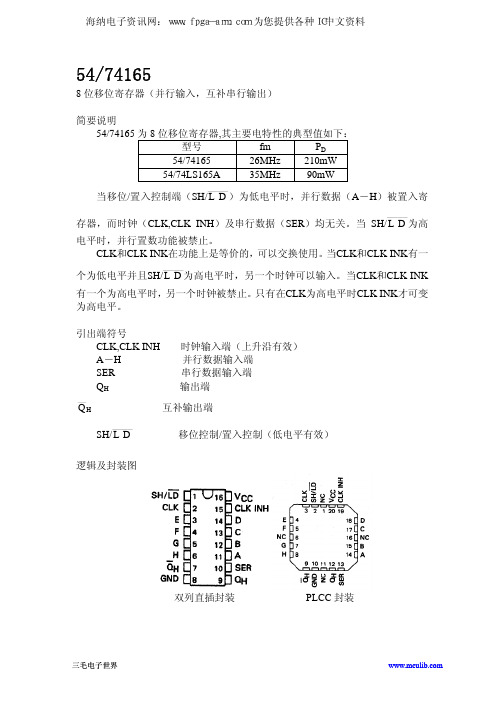
54/74165
8 位移位寄存器(并行输入,互补串行输出)
简要说明
54/74165 为 8 位移位寄存器,其主要电特性的典型值如下:
型号
fm
PD
54/74165
26MHz 210mW
54/74LS165A
35MHz
90mW
____
参
数[2]
fmax
tPLH tPHL
→ __ _
LD
__
QH, Q H
→ tPLH
CLK
__
QH, Q H
tPHL
→ tPLH H
QH
tPHL
tPLH tPHL
→ __
H QH
测试条件 Vcc =5V,CL=15Pf,RL=400Ω
‘165
最小 24
最大
31
40 24
31 17 36 27 27
- 1、下载文档前请自行甄别文档内容的完整性,平台不提供额外的编辑、内容补充、找答案等附加服务。
- 2、"仅部分预览"的文档,不可在线预览部分如存在完整性等问题,可反馈申请退款(可完整预览的文档不适用该条件!)。
- 3、如文档侵犯您的权益,请联系客服反馈,我们会尽快为您处理(人工客服工作时间:9:00-18:30)。
DATA SHEETProduct specificationFile under Integrated Circuits, IC06December 199074HC/HCT1658-bit parallel-in/serial-out shift registerFor a complete data sheet, please also download:•The IC06 74HC/HCT/HCU/HCMOS Logic Family Specifications •The IC06 74HC/HCT/HCU/HCMOS Logic Package Information •The IC06 74HC/HCT/HCU/HCMOS Logic Package OutlinesFEATURES•Asynchronous 8-bit parallel load •Synchronous serial input •Output capability: standard •I CC category: MSI GENERAL DESCRIPTIONThe 74HC/HCT165 are high-speed Si-gate CMOS devices and are pin compatible with low power Schottky TTL (LSTTL). They are specified in compliance with JEDEC standard no. 7A.The 74HC/HCT165 are 8-bit parallel-load or serial-in shift registers with complementary serial outputs (Q 7and Q 7)available from the last stage. When the parallel load (PL)input is LOW, parallel data from the D 0toD 7inputs are loaded into the register asynchronously.When PL is HIGH, data enters the register serially at the D s input and shifts one place to the right(Q 0→Q 1→Q 2,etc.) with each positive-going clock transition. This feature allows parallel-to-serial converter expansion by tying the Q 7output to the D S input of the succeeding stage.The clock input is a gated-OR structure which allows one input to be used as an active LOW clock enable (CE)input.The pin assignment for the CP and CE inputs is arbitrary and can be reversed for layout convenience. The LOW-to-HIGH transition of input CE should only take place while CP HIGH for predictable operation. Either the CP or the CE should be HIGH before theLOW-to-HIGH transition of PL to prevent shifting the data when PL is activated.APPLICATIONS•Parallel-to-serial data conversionQUICK REFERENCE DATAGND = 0 V; T amb = 25°C; t r = t f = 6 ns Notes1.C PD is used to determine the dynamic power dissipation (P D in µW):P D = C PD ×V CC 2×f i +∑(C L ×V CC 2×f o )where:f i = input frequency in MHz f o = output frequency in MHz ∑(C L ×V CC 2×f o )= sum of outputs C L =output load capacitance in pF V CC =supply voltage in V2.For HC the condition is V I = GND to V CCFor HCT the condition is V I = GND to V CC −1.5 V ORDERING INFORMATIONSee “74HC/HCT/HCU/HCMOS Logic Package Information”.SYMBOL PARAMETERCONDITIONS TYPICAL UNITHCHCTt PHL / t PLHpropagation delay CP to Q 7,Q 7PL to Q 7,Q 7D 7 to Q 7,Q 7C L = 15 pF; V CC = 5 V161511141711ns ns ns f max maximum clock frequency 5648MHz C I input capacitance3.5 3.5pF C PD power dissipation capacitance per packagenotes 1 and 23535pFPIN DESCRIPTIONPIN NO.SYMBOL NAME AND FUNCTION1PL asynchronous parallel load input (active LOW)7Q7complementary output from the last stage9Q7serial output from the last stage2CP clock input (LOW-to-HIGH edge-triggered)8GND ground (0 V)10D s serial data input11, 12, 13, 14, 3, 4, 5, 6D0to D7parallel data inputs15CE clock enable input (active LOW)16V CC positive supply voltageFig.1 Pin configuration.Fig.2 Logic symbol.Fig.3 IEC logic symbol.FUNCTION TABLE Note1.H = HIGH voltage levelh = HIGH voltage level one set-up time prior to the LOW-to-HIGH clock transition L = LOW voltage levelI =LOW voltage level one set-up time prior to the LOW-to-HIGH clock transitionq =lower case letters indicate the state of the referenced output one set-up time prior to theLOW-to-HIGH clock transition X = don’t care↑=LOW-to-HIGH clock transitionOPERATING MODESINPUTS Q n REGISTERS OUTPUTS PLCECPD SD 0-D 7Q 0Q 1-Q 6Q 7Q 7parallel load L L X X X X X X L H L H L - L H - H L H H L serial shift H H L L ↑↑l h X X L H q 0-q 5q 0-q 5q 6q 6q 6q 6hold “do nothing”HH X X X q 0q 1-q 6q 7q 7Fig.4 Functional diagram.Fig.5 Logic diagram.DC CHARACTERISTICS FOR 74HCFor the DC characteristics see“74HC/HCT/HCU/HCMOS Logic Family Specifications”. Output capability: standardI CC category: MSIAC CHARACTERISTICS FOR HCGND = 0 V; t r= t f= 6 ns; C L= 50 pFSYMBOL PARAMETERT amb(°C)UNITTEST CONDITIONS74HCV CC(V)WAVEFORMS +25−40to+85−40to+125min.typ.max.min.max.min.max.t PHL/ t PLH propagation delayCE,CP to Q7,Q7521915165332820541352505043ns 2.04.56.0Fig.6t PHL/ t PLH propagation delayPL to Q7,Q7501814165332820541352505043ns 2.04.56.0Fig.6t PHL/ t PLH propagation delayD7to Q7,Q7361310120242015030261803631ns 2.04.56.0Fig.6t THL/ t TLH output transitiontime 19767515139519161102219ns 2.04.56.0Fig.6t W clock pulse widthHIGH or LOW 801614176510020171202420ns 2.04.56.0Fig.6t W parallel load pulsewidth; LOW 801614145410020171202420ns 2.04.56.0Fig.6t rem removal timePL to CP,CE 1002017228612525211503026ns 2.04.56.0Fig.6t su set-up timeD s to CP,CE 801614114310020171202420ns 2.04.56.0Fig.6t su set-up timeCE to CP;CP to CE 801614176510020171202420ns 2.04.56.0Fig.6t su set-up timeD n to PL 801614228610020171202420ns 2.04.56.0Fig.6t h hold timeD s to CP,CED n to PL 555622555555ns 2.04.56.0Fig.6t h hold timeCE to CPCP to CE 555−17−6−5555555ns 2.04.56.0Fig.6f max maximum clockpulse frequency 630351751615242842024MHz 2.04.56.0Fig.6SYMBOL PARAMETERT amb(°C)UNITTEST CONDITIONS74HCV CC(V)WAVEFORMS +25−40to+85−40to+125min.typ.max.min.max.min.max.DC CHARACTERISTICS FOR 74HCTFor the DC characteristics see“74HC/HCT/HCU/HCMOS Logic Family Specifications”.Output capability: standardI CC category: MSINote to HCT typesThe value of additional quiescent supply current (∆I CC)for a unit load of 1 is given in the family specifications. To determine∆I CC per input, multiply this value by the unit load coefficient shown in the table below.INPUT UNIT LOAD COEFFICIENTD n D s CP CE PL 0.35 0.35 0.65 0.65 0.65AC CHARACTERISTICS FOR 74HCT GND = 0 V; t r= t f= 6 ns; C L= 50 pFSYMBOL PARAMETERT amb(°C)UNITTEST CONDITIONS74HCTV CC(V)WAVEFORMS +25−40to+85−40to+125min.typ.max.min.max.min.max.t PHL/ t PLH propagation delayCE,CP to Q7,Q717344351ns 4.5Fig.6t PHL/ t PLH propagation delayPL to Q7,Q720405060ns 4.5Fig.6t PHL/ t PLH propagation delayD7to Q7,Q714283542ns 4.5Fig.6 t THL/ t TLH output transition time7151922ns 4.5Fig.6t W clock pulse widthHIGH or LOW1662024ns 4.5Fig.6t W parallel load pulsewidth; LOW2092530ns 4.5Fig.6t rem removal timePL to CP,CE2082530ns 4.5Fig.6t su set-up timeD s to CP,CE2022530ns 4.5Fig.6t su set-up timeCE to CP; CP to CE2072530ns 4.5Fig.6t su set-up timeD n to PL20102530ns 4.5Fig.6t h hold timeD s to CP,CE;D n to PL7−1911ns 4.5Fig.6t h hold timeCE to CP, CP to CE0−700ns 4.5Fig.6f max maximum clock pulsefrequency26442117MHz 4.5Fig.6AC WAVEFORMSThe changing to output assumes internal Q6opposite state from Q7.(1)HC: V M= 50%; V I= GND to V CC.HCT:V M= 1.3 V; V I=GND to 3 V.Fig.6Waveforms showing the clock (CP) to output (Q7or Q7) propagation delays, the clock pulse width, the output transition times and the maximum clock frequency.The changing to output assumes internal Q6opposite state from Q7.(1)HC: V M= 50%; V I= GND to V CC.HCT:V M= 1.3 V; V I =GND to 3 V.Fig.7Waveforms showing the parallel load (PL) pulse width, the parallel load to output (Q7or Q7)propagation delays, the parallel load to clock (CP) and clock enable (CE) removal time.(1)HC: V M= 50%; V I= GND to V CC.HCT:V M= 1.3 V; V I=GND to 3 V.Fig.8 Waveforms showing the data input (D n)to output (Q7or Q7)propagation delays when PL is LOW.CE may change only from HIGH-to-LOW while CPis LOW.The shaded areas indicate when the input ispermitted to change for predictable outputperformance.(1)HC: V M= 50%; V I= GND to V CC.HCT:V M= 1.3 V; V I=GND to 3 V.Fig.9Waveforms showing the set-up and hold times from the serial data input (D s)to the clock (CP)and clock enable (CE)inputs, from the clock enable input (CE)to the clock input (CP)and from the clock input (CP) to the clock enable input (CE).(1)HC: V M= 50%; V I= GND to V CC.HCT:V M= 1.3 V; V I=GND to 3 V.Fig.10 Waveforms showing the set-up and hold times from the data inputs (D n)to the parallel load input (PL).PACKAGE OUTLINESSee“74HC/HCT/HCU/HCMOS Logic Package Outlines”.。