IGBT latch up effect
igbt米勒效应

igbt米勒效应
igbt米勒效应是一种与传统晶体管不同的微电子元件。
它主要由三大部分组成:发射极导通晶体管(TRA)、输出晶体管(GTO)和拓扑晶体管(TOP)。
它的工作原理是,当TRA在一个特定的高压状态下,它会从输出晶体管中释放出微小的电流以帮助偏置拓扑晶体管。
当拓扑晶体管的偏置电流获得足够的强度时,它就会切换到稳态,产生有效的可控高压脉冲。
igbt米勒效应的最大优势就在于它可以在短时间内提供大量的功率。
在高功率,高频率的场合下,它可以比传统的晶体管提供更多的功率。
这样一来,它可以应用于激光焊接、电动汽车等高功耗设备上,提供更加高效和准确的操作。
此外,igbt米勒效应还可用于可控器件(如脉冲电源)的制造,使更多的脉冲输出可能。
它的脉宽可调整,可以根据应用的需要进行调整,从而实现有效的可控制。
再者,igbt米勒效应的功耗更低,比传统晶体管耗电量降低了40%以上。
除此之外,它也比晶体管具有更高的抗干扰能力。
因此,它能够有效抑制各种外界干扰,保证电路的稳定性。
最后,igbt米勒效应的输出电压可在0-1000V之间进行调整,可以满足多种应用的要求。
它的工作温度可以从-40到125度之间调整,处于模拟和数字两种电路的需求。
总之,igbt米勒效应是一种非常成熟的微电子元件,具备多种优势,能够满足多种不同的应用要求。
它不仅可以提供高效率和高可
靠性,而且还可以抗各种外界干扰,保证电路的稳定可靠性。
因此,igbt米勒效应在微电子元件领域非常受欢迎,有望在未来成为微电子元件的主流应用。
latch-up闩锁效应
• Latch up 的定义 • Latch up 的原理分析 • 产生 Latch up 的具体原因 • 防止 Latch up 的方法
Latch up 的定义
Latch up 最易产生在易受外部干扰的I/O电路处, 也偶尔 发生在内部电路
Latch up 是指cmos晶片中, 在电源power VDD和地线 GND(VSS)之间由于寄生的PNP和NPN双极性BJT相互 影响而产生的一低阻抗通路, 它的存在会使VDD和 GND之间产生大电流
BJT到低阻基体上的通路 • 使用Guard ring: P+ ring环绕nmos并接GND;N+ ring环绕pmos 并
接VDD,一方面可以降低Rwell和Rsub的阻值,另一方面可阻止 栽子到达BJT的基极。如果可能,可再增加两圈ring。 • Substrate contact和well contact应尽量靠近source,以降低Rwell和 Rsub的阻值。 • 使nmos尽量靠近GND,pmos尽量靠近VDD,保持足够的距离在 pmos 和nmos之间以降低引发SCR的可能 • 除在I/O处需采取防Latch up的措施外,凡接I/O的内部mos 也应圈 guard ring。 • I/O处尽量不使用pmos(nwell)
• Emitter-Base齐纳管有100~300欧姆的 内阻, NSD/P-epi和PSD/N-well齐纳 管的内阻则更大,这些内阻大大提高 了齐纳管的耐压性,同时也会使PAD 上出现高于理论值几十伏的电压,这 种特点大大限制了齐纳箝位保护电路 的应用。
PAD
D1
NMoat
Metal connecting to pad
Poly resistor
IGBT芯片技术发展概述
IGBT芯片技术发展概述摘要:回顾IGBT芯片技术的发展历程,从最开始发明,经过不断研究,目前已经广泛的应用在工业控制、电动汽车、轨道交通、智能电网、变频家电中。
本文着重介绍了IGBT芯片技术发展历程中,不同时期解决的技术难题,包括闩锁问题、IGBT关断拖尾、降低饱和压降等,以及未来的发展展望。
关键字:IGBT; RC-IGBT; CS-TBT; SJ-IGBT; SIC-IGBTOverview of IGBT chip technology developmentAbstract: Reviewing the development history of IGBT chip technology, after continuous research from the beginning, it has been widely used in industrial control, electric vehicles, rail transit, smart grid and frequency conversion equipment. This article focuses on the technical problems solved in different periods during the development of IGBT chip technology, including latch-up problems, IGBT turn-off tailing, reduction of saturation voltage drop, etc., as well as future development prospects.Keywords: IGBT; RC-IGBT; CS-TBT; SJ-IGBT; SIC-IGBT图1 IGBT Latch-Up示意图图2 Non-Latch-Up IGBT器件结构至此,IGBT进入快速发展的阶段,多家厂商成功量产出IGBT,并不断迭代升级。
IGBT器件分析(实用经验)
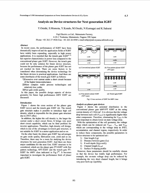
Abstract In recent years, the performances of IGBT have been dramatically improved and the application fields of IGBT have widely been expanding, especially in high power applications. It is reported that the trench gate IGBT"'3' has superior characteristics in power loss compared to the conventional planer gate IGBT. However, the trench gate could not be only solution for future device structure, because the performance of the planer gate IGBT has not yet reached its limit. There are some factors to be considered when determining the device technology for the future devices in practical applications. And there are some drawbacks of the trench gate IGBT as follows: 1)Excessive over current under a short circuit because of the higher transconductance. 2)More complex wafer process technologies and relatively low yields. 3)POOr gate oxide quality. In this paper, the possible design aspects of device geometry for hture high performance 600V IGBT are discussed. Introduction Figure 1 shows the cross section of the planer gate IGBT (a)-(c) and the trench gate IGBT (d). The trench gate structure makes it possible to introduce high cell density, which is impossible for the planer gate structure due to JFET effect. In addition, the higher the cell density is, the larger the current under a short circuit flows, It brings very poor short circuit capability, which can be fatal problem for inverter applications. Therefore, high density cell design, whch is one of the ;advantagesin trench gate structure, is not suitable for IGBT in a motor application and so on. On the other hand, the planer gate IGBT has advantages on gate oxide quality, fabrication cost, yield and so on. Therefore, there may be a room for studying the device structures for next generation IGBT. And there are three major candidates for the next Gen. IGBT structure to be considered, which are the planer gate PT-IGBT with fine pattern technology, NPT-IGBT and the trench gate PTIGBT for 600V class indicated in Fig.l'4'. It becomes important to investigate the performance limit of planer gate IGBT.
高速IGBT及IGBT抗闩锁性能优化

摘要摘要文章从技术发展角度总结了IGBT发明初期的发展历史,比较全面的介绍了动态控制IGBT阳极发射结的研究进展与现状,并列举了目前比较常见的能提高IGBT抗闩锁能力的设计方法。
采用MEDICI电路仿真功能模拟研究基于陈星弼教授的专利--一种高速IGBT[27]而设计的两种高速IGBT结构。
利用专利中给出的技术所设计的高速IGBT,在开关过程中依靠独特的终端设计结构,能在内部生成合适的阶跃信号(阶跃电平)并反馈给阳极控制端,以此达到动态控制阳极发射结的短路与开路,不需要低压电源。
结果显示,高速IGBT不但能完全消除拖尾电流,并且使IGBT关断时的下降时间由18μs,变为0.8μs。
电流大小相同时,高速IGBT导通压降为1.40V 比普通IGBT的1.35V略有提升。
研究了一种新的IGBT发射极元胞并给出其设计方法。
该元胞在不影响单位面积有效沟道宽度的情况下,将P+与N+并排垂直于沟道一侧放置以缩短空穴路径。
与传统采用深P+注入的抗闩锁方法相比,经过优化设计后的新结构闩锁电流增大了约8倍;V ce=1.5V时,新元胞的电流密度比以前增加了3倍;元胞静态阻断电压也有20%的增加,从而扩展了IGBT的安全工作区,而且工艺更简单。
关键词:绝缘栅双极型晶体管动态控制阳极双栅IGBT 闩锁IABSTRACTABSTRACTThe article summarizes the development history of the early invention of IGBT from the point of technical development, and introduces the progress and status of dynamic control of IGBT anode emitter more comprehensively, and lists the current common design methods which can improve the latch-up immunity of IGBT.The advanced circuit module in MEDICI is used to study the two kinds of structures of high-speed IGBT, both of which are designed based on the patent --a high speed IGBT [27] by Professor Xingbi Chen. The high-speed IGBT can achieve dynamic control of the anode, and the appropriate step control signal is generated by the unique structure of the voltage terminal can generate appropriate anode control signal, without the help of the low voltage supply. The simulation result shows that, the proposed high speed IGBT has elimited the current tail, and the turn-off time has been largely reduced, from original 18μs to 0.8μs. However, the on-state voltage drop of this high speed IGBT is 1.4V, which is little larger than the compared common structure with 1.35V forward voltage drop.A new kind of cell of IGBT emitter is studied and the design method is given. The cell places p+ and n+ side by side and perpendicular to one side of the channel in order to shorten the path of holes without affecting the effective channel width per unit area. Compared with traditional anti-latch method which uses deep injection of P+, the latch current of the new structure with optimized design is increased by about 8 times; when V ce is 1.5V, the current density of the new cell is 3 times bigger than before; and the static blocking voltage of the cell has also increased 20%, thus extending the safe operating area of IGBT and simplifying the technology at the same time.Keywords:IGBT Dynamic controlled anode-short DGIGBT Latch-upII目录摘要 (I)ABSTRACT ..................................................................................................................... I I 目录 .. (III)第一章绪论 (1)1.1功率器件发展简介 (1)1.2 IGBT产生背景及发展历史 (2)1.3 IGBT的总体发展趋势 (5)1.4国内外IGBT发展现状 (7)1.5本章小结 (9)第二章IGBT结构及工作机理 (10)2.1 IGBT端口命名的说明 (10)2.2 穿通型IGBT和非穿通型IGBT (11)2.3 IGBT工作模式 (15)2.3.1反向耐压特性 (15)2.3.2 正向阻断特性 (16)2.3.3 正向导通特性 (16)2.3.4 IGBT的开启与关断 (17)2.4 关于IGBT性能的优化 (19)2.4.1 导通压降与关断时间之间的折衷关系 (19)2.4.2 关于IGBT的抗闩锁能力 (23)2.5 第二章小结 (25)第三章高速IGBT的研究与设计 (26)3.1 MEDICI简介 (26)3.1.1 MEDICI所采用的半导体物理方程 (26)3.1.2 模型选择与比较 (27)3.2 动态阳极控制的IGBT研究背景 (29)3.3高速IGBT的研究与设计 (33)3.4 本章小结 (42)III第四章IGBT抗闩锁性能优化 (43)4.1 IGBT静态与动态闩锁机理分析 (43)4.2不同的抗闩锁结构简述 (44)4.3 新结构抗闩锁性能仿真分析 (49)4.4 本章小结 (57)第五章结论 (59)5.1论文工作总结 (59)5.2工作改进方向 (59)致谢 (61)参考文献 (63)攻读硕士期间取得的研究成果 (68)IV第一章绪论第一章绪论本章介绍功率半导体科学技术的作用与发展。
IGBT短路保护中的软关断技术分析
It is very common that an IGBT used for motor drive, UPS and some other industrial applications, be selected for 10 micro-second short-circuit withstand time (SCWT) if regular de-sat protection driver is used. But this driver generates high turn-off stress to the IGBT during inverter short circuit or the output becomes faulty. Under these abnor-mal conditions when the IGBT is turned-off abruptly, failures can occur if the IGBT is not selected properly. If the smart fault protection is not used, high turn-off loss will be generated and even short circuit current can ramp-up to a dangerous level destroying the IGBT. There are several ways to turn-off the IGBT once fault condition is detected. Some of these are as follows:Gate is discharged through high gate resistance. This discharge path is activated only during the above said abnormal conditions. This is not the best solution.Gate voltage is abruptly reduced to zero.Adding some source inductance which is common for both gate dis-charge path and load current.Gate de-bias occurs. But during normal condition switching loss is increased.Sense IGBT can also be used where fault current is sensed by pilot cell but the current sense accuracy of these pilot cells is not good which is further is affected by temperature.Gate voltage pattern analyzer for short-circuit protection in IGBT inverters [1]. These circuits are very sensitive to load changes and type of loads.Current sense resistor or Hall-effect devices are also used to detect fault through IGBT. But again these methods either generate power loss or are costly.But de-sat protection is the most commonly used for short-circuit and over current fault protection. De-sat detection truly provides the state of electrical over stress of IGBT under current fault condition when gate voltage is high. Reducing gate voltage in a controlled manner to just above gate threshold voltage is preferred and described in this article. This will reduce fault current and after some finite time gate voltage is brought down to zero safely, turning-off the IGBT without stress.Gate Drive CircuitThe main function of any gate driver circuit is to convert a control sig-nal to a power signal that can efficiently controls the IGBT or MOS-FET turn-on and turn-off. If the IGBT or MOSFET requires short cir-cuit protection, the gate drive circuit must safely turn-off the switch during a shorted or abnormal overload condition. A more detailed list of the gate drive circuit requirements for an IGBT or MOSFET are as follows:A controlled turn-on and turn-off of the IGBT so as to optimize the conduction and switching losses.In some applications, electrical isolation between control circuit and power circuit is very important.In the case of a short circuit condition, the IGBT should be protected and turned-off safely with minimum power dissipation and stress. The gate drive circuit should be able to minimize short circuit current and short-circuit withstand time without device failure. If both of these parameters are minimized, the power dissipation under short circuit will reduce and the system reliability will increase.During a short circuit condition, the IGBT collector to emitter voltage can rise fast. The voltage across the gate to emitter should not beIGBT Behavior under Short Circuit and Fault ProtectionUsing Two-Step-Soft-Turn-Off Gate DriverIn inverter driven UPS or motor applications, the IGBT can be destroyed when it is turned-on into a faulted motor or an output short circuit or an input bus voltage shoot through. Under these conditions current through the IGBT increases rapidly until it saturates. After fault detection, depending on the point at which the fast turn-off pulse is applied, very different levels of hole current can flow under the n+ source region, making this an important factor in the successful containment of the fault current. We present experimental observations showing that IGBT failure under short-circuit conditions is dependent on where and how the turn-off pulse is applied. A two-step (two-level) turn-off gate driver circuit is introduced which safely turns-off even a high transconductance IGBT during short-circuit and abnormal over current faults. This turn-off process startsduring faulted condition only.By Sampat Shekhawat and Bob Brockway, Fairchild SemiconductorIGBT驱动的软关断技术分析35allowed to rise due to gate to collector displacement current flowinginto the gate to emitter capacitance, Cge. Current flowing into Cge will cause Vge to rise and further increase the short circuit current.One should make sure that this condition is avoided.Preferably a totem pole output stage with separate turn-on and turn-off resistance option. The gate discharging switch of the totem pole should be as close as possible to IGBT and minimize the loop induc-tance between this switch and IGBT gate & emitter terminals. Minimize the propagation delay time between input and output pulses of the gate driver.De-SaturationThe de-saturation detection technique for identifying a short circuit and fault condition in an IGBT is well known. Generally, a de-satura-tion condition is said to exist if the voltage across the IGBT collector to emitter terminals rises above 5-8 volts while the gate to emitter voltage is high. This condition indicates that the current through the IGBT has exceeded the normal operating level. The gate drive circuit should be designed so that it reacts promptly to the short circuit and safely turns-off the IGBT within SCWT rating of the IGBT. However, in recent years, IGBTs have been designed with lower conduction and switching losses but this generally reduces SCWT. IGBT technology utilizes shallow junctions to decrease switching and conduction loss-es. However these new technologies have increased the transcon-ductance (gm) of the IGBT. Since the magnitude of the IGBT short circuit current is directly proportional to gm, during a short-circuit con-dition, a higher collector current results. The large collector current and high bus voltage place the IGBT in a state of high instantaneous power dissipation that can only be sustained for a few microseconds.The gate drive circuit must respond very quickly and efficiently to the fault current to protect the IGBT. Due to the two-step turn-off, the IGBT with even 4 microseconds short circuit withstand time can safe-ly be turned-off and protected. The IGBT, used in conjunction with the two-step turn-off gate drive, safely turns off low impedance over-cur-rent faults and shorted bus conditions where single-step gate drivers fail. The Industry standard (10 µs) SCWT is no longer required when the IGBT is used with this gate driver.IGBT Behavior during short circuit and over currentThe peak current during a short circuit is limited by the gm of the IGBT. Moreover, the rate of rise of the current is limited by the turn-on characteristics of the IGBT in combination with common emitter inductance. If IGBT collector current does not saturate and reach a state of equilibrium and bus voltage has not raised high enough attempting to turn off the IGBT during can lead to IGBT latch-up [2].In case of fault conditions very different hole current flow under n+source regions. These different hole current conditions and patterns of hole current under n+ source generate different electrical stress. In case if the gate voltage is brought down abruptly to zero before device voltage reaches clamp, the IGBT can latch-up and fail. Flow of electron through the channel is cutoff once the gate is turned off.Holes continue to inject from emitter of p-n-p structure which isknown as IGBT collector. This process stops when electrons in IGBT N-base are depleted. At this point IGBT current is almost all hole cur-rent. The amount of holes is very high here and if IGBT does not reach clamp voltage IGBT can latch-up and fail. However if enough time is allowed to complete this process and plasma of electrons in IGBT N-base is reduced or depleted so that base current reaches zero. At this point the carriers from emitter of IGBT p-n-p transistor are no longer injected and IGBT current is almost all hole current.IGBT voltage rises at a rate so that edge of the depletion spread cansweep out enough carriers to maintain inductive current. If enough time is allowed to stabilize the bus voltage while the channel current is flowing, the IGBT N-base is depleted and because of this current flow is more uniformly distributed. The displacement current becomes very small since dv/dt reduces and latch-up is avoided. If enoughtime is not allowed for the IGBT to reach clamp voltage and gate volt-age is removed abruptly, IGBT voltage will rise with high dv/dt and current in IGBT is non-uniformly distributed, high displacement cur-rent generated by high dv/dt can latch-up IGBT. Non-uniform gate ESR combined with Miller capacitance result in non-uniform turn-off of IGBT active area. This results into high localized hole current den-sity flowing laterally in P-base of parasitic n-p-n bipolar resulting in latch-up of parasitic thyristor. Because of these reasons one has to wait untill IGBT reaches clamp voltage collector current saturates. So it is safer to choose IGBT with 10 microseconds SCWT for motor drive and UPS inverter applications if a regular gate driver is used.Two step soft turn-off gate driveIt is clear that if the collector to emitter voltage rises to the DC Bus slowly and high transconductance increases short circuit current, reg-ular driver does not protect an IGBT with a low short circuit withstand time (<5us). However the longer SCWT comes at the cost of higher switching and conduction losses. The rate of rise of the collector to emitter voltage is dependent upon the operating conditions and can take several microseconds to rise to bus voltage. However, the gate drive must respond quickly to initiate turn off to protect a low SCWT IGBT. The only solution is to lower the gate voltage to just above threshold voltage of the IGBT. The IGBT reaches clamp voltage faster and reduces IGBT current during fault.The schematic of two step gate driver is shown in Figure 1. The gate driver output will produce a positive signal with respect to the IGBT emitter terminal when the control signal goes high. As the control sig-nal goes high, transistor Q1 turns on, Q2 turns off, and the LED of optocoupler U1 turns on. This forces the output voltage of the opto-coupler to the low state. When the optocoupler output goes low, both transistors Q3 and Q4 turn off, turning on the Darlington combination of transistors Q5 and Q7. This will connect the Von supply to the gate of the IGBT through the gate turn-on resistor initiating the IGBT turn-on process.During the time that transistor Q4 is off, the output stage PNP tran-sistor Q6 remains off. Once the IGBT is turned on, the inverting inputFigure 1: Two-step gate drive circuitof comparator U3 will be clamped to one diode drop (forward voltage drop of de-saturation diode DC) plus the IGBT Vcesat voltage. For the gate driver to operate properly, the inverting voltage node must be at a lower voltage level than the non-inverting voltage node. The non-inverting input voltage is set by zener diode Z2. When the con-trol signal goes low, the LED of U1 turns off, and the optocoupler out-put voltage Von goes high with respect to negative terminal of VccG.This turns on transistors Q3 and Q4. When Q3 turns on, capacitor C5discharges through R24 allowing the output of the comparator U3 to remain high. Once transistor Q4 is on, the output stage Darlington combination turns off, and the PNP transistor Q6 turns on. Now, the gate of the IGBT will discharge through R21, R22 and transistor Q6,initiating the IGBT turn-off. During normal operation (no short-circuit or overload condition) comparator U3 remains off without effecting the gate driver circuit.However, the de-saturation circuit activates when a fault occurs at the inverter output, or the complimentary IGBT turns on due to noise.When the IGBT is turned-on into the low impedance load, it draws a large current, which causes the collector to emitter voltage of the IGBT to rise towards the bus voltage. As the IGBT collector to emit-ter voltage rises, the voltage across capacitor C5 will begin to charge towards VccG.When the voltage across C5 rises above Z2 zener voltage, the com-parator U3 turns-on. When U3 turns on, the base voltage of Darling-ton transistor Q5 lowers to approximately 8 volts with some quick slope. R14, R15, R27, C6 and D2 set this voltage and slope. The applied gate voltage of the IGBT is reduced from approximately 13volts to about 8 volts, significantly decreasing the saturation current of the IGBT. As soon as the gate bias reduces, electron current (MOSFET current) reduces. As electron current reduces, base cur-rent of the IGBT structure PNP transistor reduces. Hence, the satura-tion current of the IGBT reduces.When IGBT is turned-on into an inductive short-circuit or it is under shoot through condition current ramps quickly. The voltage across the device increases and current through the IGBT saturates if the gate voltage is kept on. Now if the gate voltage is brought to zero after IGBT current saturates and drain voltage rises to clamp voltage the IGBT will turn-off safely.The Ic U4 & U5 decide the time duration of first step level voltage and after this time the comparator U2 turns on and transistor Q5 &Q7 turn-off and Q6 turns-on turning-off IGBT safely. During first step time, the collector to emitter voltage across the IGBT rises faster than it would by holding the gate at 15 volts. As previously mentioned, the faster collector to emitter voltage rise is beneficial for the IGBT to safely turn-off the IGBT under a shorted load.Figure 2 and Figure 3 depicts the Fairchild 1200V Trench IGBT turn-ing on into a resistive load and after 1 micro-second the resistor is shorted. In ‘case 1’IGBT is protected within 2.6 micro-seconds. The zener Z2 decides when to start first step. The second step voltage level is decided by D1 and Vbe of gate turn-on transistor as shown in figure 2. When the zener Z2 value is 8.2V, that allows IGBT peak cur-rent to rise up to about 300A but still it turns-off IGBT safely asshown figure 2 ‘case 1’. But in figure 3 ‘case 2’when this zener value is reduced to 5.6 volts the short circuit current only rises up to about 190A. By selecting this zener properly depending on type of IGBT technology one can reduce this short circuit peak current and increase system reliability.SummaryA new two-step gate drive circuit has been proposed which protects the IGBT during short circuit and over load fault. The gate-drive safe-ly turns-off the IGBT in two steps. The IGBT stress during short cir-cuit or fault current conditions is minimized. The new gate drive cir-cuit can safely shut-off IGBTs with SCWT as low as 3?sec. The Fairchild trench IGBT can be turned-off safely in less than 3 micro-seconds.REFERENCES[1] Jun-Bae Lee, Dac-Woong Chung and Bum-Seok Suh, “Gate Volt-age Pattern Analyzer for Short-Circuit Protection in IGBT Inverters”APEC, 2007.[2] A. Bhalla, S. Shekhawat, J. Gladish, J. Yedinak, G. Dolny, “ IGBT Behavior During Short circuit and Fault Current Protection”ISPSD’98, pp. 245-248, June 3-6,1998.[3] B. Jayant Baliga, “Modern Power Devices” John Wiley & Sons”Figure 2: Trench IGBT (FGA25N120ANTD) into short circuit ‘case 1’Figure 3: Trench IGBT (FGA25N120ANTD) into short circuit ‘case 2’。
IGBT的设计要点
绝缘栅双极晶体管(IGBT )的设计要点赵善麒、张景超、刘利峰、王晓宝江苏宏微科技有限公司作为新型电力半导体器件的主要代表,IGBT 被广泛用于工业、信息、新能源、医学、交通、军事和航空领域。
随着半导体材料和加工工艺的不断进步,IGBT 的电流密度、耐压和频率不断得到提升。
目前,市场上的IGBT 器件的耐压高达6500V ,单管芯电流高达200A ,频率达到300kHz 。
在高频大功率领域,目前还没有任何一个其它器件可以代替它。
本文着重分析讨论IGBT 器件的设计要点。
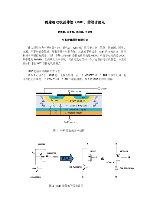
一、IGBT 的基本结构和工作原理从图1可以看出,IGBT 是一个复合器件,由一个MOSFET 和一个PNP 三极管组成,也可以把它看成是一个VDMOS 和一个PN 二极管组成。
图2是IGBT 的等效电路。
图1 IGBT 原胞的基本结构简化为 Injection layerR b图2 IGBT 器件的等效电路图1. IGBT 的 静态特性常规IGBT 只有正向阻断能力,由PNP 晶体管的集电结承担,而其反向的电压承受能力只有几十伏,因为PNP 晶体管的发射结处没有任何终端和表面造型。
IGBT 在通态情况下,除了有一个二极管的门槛电压(0.7V 左右)以外,其输出特性与VDMOS 的完全一样。
图3 一并给出了IGBT 器件的正、反向直流特性曲线。
IGBT 的主要静态参数: z 阻断电压V (BR )CES – 器件在正向阻断状态下的耐压; ; 。
z 通态压降V CE(on) – 器件在导通状态下的电压降z 阈值电压V GEth – 器件从阻断状态到导通状态所需施加的栅极电压 V G图3 IGBT 器件的正、反向直流特性2. IGBT 的开关特性IGBT 的开关机理与VDMOS 完全一样,由MOS 栅来控制其开通和关断。
所不同 的是IGBT 比VDMOS 在漏极多了一个PN 结,在导通过程中有少子空穴的参与,这就是所谓的电导调制效应。
IGBT短路保护中的软关断技术分析
It is very common that an IGBT used for motor drive, UPS and some other industrial applications, be selected for 10 micro-second short-circuit withstand time (SCWT) if regular de-sat protection driver is used. But this driver generates high turn-off stress to the IGBT during inverter short circuit or the output becomes faulty. Under these abnor-mal conditions when the IGBT is turned-off abruptly, failures can occur if the IGBT is not selected properly. If the smart fault protection is not used, high turn-off loss will be generated and even short circuit current can ramp-up to a dangerous level destroying the IGBT. There are several ways to turn-off the IGBT once fault condition is detected. Some of these are as follows:Gate is discharged through high gate resistance. This discharge path is activated only during the above said abnormal conditions. This is not the best solution.Gate voltage is abruptly reduced to zero.Adding some source inductance which is common for both gate dis-charge path and load current.Gate de-bias occurs. But during normal condition switching loss is increased.Sense IGBT can also be used where fault current is sensed by pilot cell but the current sense accuracy of these pilot cells is not good which is further is affected by temperature.Gate voltage pattern analyzer for short-circuit protection in IGBT inverters [1]. These circuits are very sensitive to load changes and type of loads.Current sense resistor or Hall-effect devices are also used to detect fault through IGBT. But again these methods either generate power loss or are costly.But de-sat protection is the most commonly used for short-circuit and over current fault protection. De-sat detection truly provides the state of electrical over stress of IGBT under current fault condition when gate voltage is high. Reducing gate voltage in a controlled manner to just above gate threshold voltage is preferred and described in this article. This will reduce fault current and after some finite time gate voltage is brought down to zero safely, turning-off the IGBT without stress.Gate Drive CircuitThe main function of any gate driver circuit is to convert a control sig-nal to a power signal that can efficiently controls the IGBT or MOS-FET turn-on and turn-off. If the IGBT or MOSFET requires short cir-cuit protection, the gate drive circuit must safely turn-off the switch during a shorted or abnormal overload condition. A more detailed list of the gate drive circuit requirements for an IGBT or MOSFET are as follows:A controlled turn-on and turn-off of the IGBT so as to optimize the conduction and switching losses.In some applications, electrical isolation between control circuit and power circuit is very important.In the case of a short circuit condition, the IGBT should be protected and turned-off safely with minimum power dissipation and stress. The gate drive circuit should be able to minimize short circuit current and short-circuit withstand time without device failure. If both of these parameters are minimized, the power dissipation under short circuit will reduce and the system reliability will increase.During a short circuit condition, the IGBT collector to emitter voltage can rise fast. The voltage across the gate to emitter should not beIGBT Behavior under Short Circuit and Fault ProtectionUsing Two-Step-Soft-Turn-Off Gate DriverIn inverter driven UPS or motor applications, the IGBT can be destroyed when it is turned-on into a faulted motor or an output short circuit or an input bus voltage shoot through. Under these conditions current through the IGBT increases rapidly until it saturates. After fault detection, depending on the point at which the fast turn-off pulse is applied, very different levels of hole current can flow under the n+ source region, making this an important factor in the successful containment of the fault current. We present experimental observations showing that IGBT failure under short-circuit conditions is dependent on where and how the turn-off pulse is applied. A two-step (two-level) turn-off gate driver circuit is introduced which safely turns-off even a high transconductance IGBT during short-circuit and abnormal over current faults. This turn-off process startsduring faulted condition only.By Sampat Shekhawat and Bob Brockway, Fairchild SemiconductorIGBT驱动的软关断技术分析35allowed to rise due to gate to collector displacement current flowinginto the gate to emitter capacitance, Cge. Current flowing into Cge will cause Vge to rise and further increase the short circuit current.One should make sure that this condition is avoided.Preferably a totem pole output stage with separate turn-on and turn-off resistance option. The gate discharging switch of the totem pole should be as close as possible to IGBT and minimize the loop induc-tance between this switch and IGBT gate & emitter terminals. Minimize the propagation delay time between input and output pulses of the gate driver.De-SaturationThe de-saturation detection technique for identifying a short circuit and fault condition in an IGBT is well known. Generally, a de-satura-tion condition is said to exist if the voltage across the IGBT collector to emitter terminals rises above 5-8 volts while the gate to emitter voltage is high. This condition indicates that the current through the IGBT has exceeded the normal operating level. The gate drive circuit should be designed so that it reacts promptly to the short circuit and safely turns-off the IGBT within SCWT rating of the IGBT. However, in recent years, IGBTs have been designed with lower conduction and switching losses but this generally reduces SCWT. IGBT technology utilizes shallow junctions to decrease switching and conduction loss-es. However these new technologies have increased the transcon-ductance (gm) of the IGBT. Since the magnitude of the IGBT short circuit current is directly proportional to gm, during a short-circuit con-dition, a higher collector current results. The large collector current and high bus voltage place the IGBT in a state of high instantaneous power dissipation that can only be sustained for a few microseconds.The gate drive circuit must respond very quickly and efficiently to the fault current to protect the IGBT. Due to the two-step turn-off, the IGBT with even 4 microseconds short circuit withstand time can safe-ly be turned-off and protected. The IGBT, used in conjunction with the two-step turn-off gate drive, safely turns off low impedance over-cur-rent faults and shorted bus conditions where single-step gate drivers fail. The Industry standard (10 µs) SCWT is no longer required when the IGBT is used with this gate driver.IGBT Behavior during short circuit and over currentThe peak current during a short circuit is limited by the gm of the IGBT. Moreover, the rate of rise of the current is limited by the turn-on characteristics of the IGBT in combination with common emitter inductance. If IGBT collector current does not saturate and reach a state of equilibrium and bus voltage has not raised high enough attempting to turn off the IGBT during can lead to IGBT latch-up [2].In case of fault conditions very different hole current flow under n+source regions. These different hole current conditions and patterns of hole current under n+ source generate different electrical stress. In case if the gate voltage is brought down abruptly to zero before device voltage reaches clamp, the IGBT can latch-up and fail. Flow of electron through the channel is cutoff once the gate is turned off.Holes continue to inject from emitter of p-n-p structure which isknown as IGBT collector. This process stops when electrons in IGBT N-base are depleted. At this point IGBT current is almost all hole cur-rent. The amount of holes is very high here and if IGBT does not reach clamp voltage IGBT can latch-up and fail. However if enough time is allowed to complete this process and plasma of electrons in IGBT N-base is reduced or depleted so that base current reaches zero. At this point the carriers from emitter of IGBT p-n-p transistor are no longer injected and IGBT current is almost all hole current.IGBT voltage rises at a rate so that edge of the depletion spread cansweep out enough carriers to maintain inductive current. If enough time is allowed to stabilize the bus voltage while the channel current is flowing, the IGBT N-base is depleted and because of this current flow is more uniformly distributed. The displacement current becomes very small since dv/dt reduces and latch-up is avoided. If enoughtime is not allowed for the IGBT to reach clamp voltage and gate volt-age is removed abruptly, IGBT voltage will rise with high dv/dt and current in IGBT is non-uniformly distributed, high displacement cur-rent generated by high dv/dt can latch-up IGBT. Non-uniform gate ESR combined with Miller capacitance result in non-uniform turn-off of IGBT active area. This results into high localized hole current den-sity flowing laterally in P-base of parasitic n-p-n bipolar resulting in latch-up of parasitic thyristor. Because of these reasons one has to wait untill IGBT reaches clamp voltage collector current saturates. So it is safer to choose IGBT with 10 microseconds SCWT for motor drive and UPS inverter applications if a regular gate driver is used.Two step soft turn-off gate driveIt is clear that if the collector to emitter voltage rises to the DC Bus slowly and high transconductance increases short circuit current, reg-ular driver does not protect an IGBT with a low short circuit withstand time (<5us). However the longer SCWT comes at the cost of higher switching and conduction losses. The rate of rise of the collector to emitter voltage is dependent upon the operating conditions and can take several microseconds to rise to bus voltage. However, the gate drive must respond quickly to initiate turn off to protect a low SCWT IGBT. The only solution is to lower the gate voltage to just above threshold voltage of the IGBT. The IGBT reaches clamp voltage faster and reduces IGBT current during fault.The schematic of two step gate driver is shown in Figure 1. The gate driver output will produce a positive signal with respect to the IGBT emitter terminal when the control signal goes high. As the control sig-nal goes high, transistor Q1 turns on, Q2 turns off, and the LED of optocoupler U1 turns on. This forces the output voltage of the opto-coupler to the low state. When the optocoupler output goes low, both transistors Q3 and Q4 turn off, turning on the Darlington combination of transistors Q5 and Q7. This will connect the Von supply to the gate of the IGBT through the gate turn-on resistor initiating the IGBT turn-on process.During the time that transistor Q4 is off, the output stage PNP tran-sistor Q6 remains off. Once the IGBT is turned on, the inverting inputFigure 1: Two-step gate drive circuitof comparator U3 will be clamped to one diode drop (forward voltage drop of de-saturation diode DC) plus the IGBT Vcesat voltage. For the gate driver to operate properly, the inverting voltage node must be at a lower voltage level than the non-inverting voltage node. The non-inverting input voltage is set by zener diode Z2. When the con-trol signal goes low, the LED of U1 turns off, and the optocoupler out-put voltage Von goes high with respect to negative terminal of VccG.This turns on transistors Q3 and Q4. When Q3 turns on, capacitor C5discharges through R24 allowing the output of the comparator U3 to remain high. Once transistor Q4 is on, the output stage Darlington combination turns off, and the PNP transistor Q6 turns on. Now, the gate of the IGBT will discharge through R21, R22 and transistor Q6,initiating the IGBT turn-off. During normal operation (no short-circuit or overload condition) comparator U3 remains off without effecting the gate driver circuit.However, the de-saturation circuit activates when a fault occurs at the inverter output, or the complimentary IGBT turns on due to noise.When the IGBT is turned-on into the low impedance load, it draws a large current, which causes the collector to emitter voltage of the IGBT to rise towards the bus voltage. As the IGBT collector to emit-ter voltage rises, the voltage across capacitor C5 will begin to charge towards VccG.When the voltage across C5 rises above Z2 zener voltage, the com-parator U3 turns-on. When U3 turns on, the base voltage of Darling-ton transistor Q5 lowers to approximately 8 volts with some quick slope. R14, R15, R27, C6 and D2 set this voltage and slope. The applied gate voltage of the IGBT is reduced from approximately 13volts to about 8 volts, significantly decreasing the saturation current of the IGBT. As soon as the gate bias reduces, electron current (MOSFET current) reduces. As electron current reduces, base cur-rent of the IGBT structure PNP transistor reduces. Hence, the satura-tion current of the IGBT reduces.When IGBT is turned-on into an inductive short-circuit or it is under shoot through condition current ramps quickly. The voltage across the device increases and current through the IGBT saturates if the gate voltage is kept on. Now if the gate voltage is brought to zero after IGBT current saturates and drain voltage rises to clamp voltage the IGBT will turn-off safely.The Ic U4 & U5 decide the time duration of first step level voltage and after this time the comparator U2 turns on and transistor Q5 &Q7 turn-off and Q6 turns-on turning-off IGBT safely. During first step time, the collector to emitter voltage across the IGBT rises faster than it would by holding the gate at 15 volts. As previously mentioned, the faster collector to emitter voltage rise is beneficial for the IGBT to safely turn-off the IGBT under a shorted load.Figure 2 and Figure 3 depicts the Fairchild 1200V Trench IGBT turn-ing on into a resistive load and after 1 micro-second the resistor is shorted. In ‘case 1’IGBT is protected within 2.6 micro-seconds. The zener Z2 decides when to start first step. The second step voltage level is decided by D1 and Vbe of gate turn-on transistor as shown in figure 2. When the zener Z2 value is 8.2V, that allows IGBT peak cur-rent to rise up to about 300A but still it turns-off IGBT safely asshown figure 2 ‘case 1’. But in figure 3 ‘case 2’when this zener value is reduced to 5.6 volts the short circuit current only rises up to about 190A. By selecting this zener properly depending on type of IGBT technology one can reduce this short circuit peak current and increase system reliability.SummaryA new two-step gate drive circuit has been proposed which protects the IGBT during short circuit and over load fault. The gate-drive safe-ly turns-off the IGBT in two steps. The IGBT stress during short cir-cuit or fault current conditions is minimized. The new gate drive cir-cuit can safely shut-off IGBTs with SCWT as low as 3?sec. The Fairchild trench IGBT can be turned-off safely in less than 3 micro-seconds.REFERENCES[1] Jun-Bae Lee, Dac-Woong Chung and Bum-Seok Suh, “Gate Volt-age Pattern Analyzer for Short-Circuit Protection in IGBT Inverters”APEC, 2007.[2] A. Bhalla, S. Shekhawat, J. Gladish, J. Yedinak, G. Dolny, “ IGBT Behavior During Short circuit and Fault Current Protection”ISPSD’98, pp. 245-248, June 3-6,1998.[3] B. Jayant Baliga, “Modern Power Devices” John Wiley & Sons”Figure 2: Trench IGBT (FGA25N120ANTD) into short circuit ‘case 1’Figure 3: Trench IGBT (FGA25N120ANTD) into short circuit ‘case 2’。
- 1、下载文档前请自行甄别文档内容的完整性,平台不提供额外的编辑、内容补充、找答案等附加服务。
- 2、"仅部分预览"的文档,不可在线预览部分如存在完整性等问题,可反馈申请退款(可完整预览的文档不适用该条件!)。
- 3、如文档侵犯您的权益,请联系客服反馈,我们会尽快为您处理(人工客服工作时间:9:00-18:30)。
1英文名称编辑
Self-locking effect
2基本概念编辑
在IGBT内部寄生着一个N-PN+晶体管和作为主开关器件的P+N-P晶体管组成的寄生晶闸管。
其中NPN晶体管的基极与发射极之间存在体区短路电阻,P形体区的横向空穴电流会在该电阻上产生压降,相当于对J3结施加一个正向偏压,在额定集电极电流范围内,这个偏压很小,不足以使J3开通,然而一旦J3开通,栅极就会失去对集电极电流的控制作用,导致集电极电流增大,造成器件功耗过高而损坏。
这种电流失控的现象,就像普通晶闸管被触发以后,即使撤销触发信号晶闸管仍然因进入正反馈过程而维持导通的机理一样,因此被称为擎住效应或自锁效应。
3原因编辑
除过大的ic可能产生擎住效应外,当IGBT处于截止状态时,如果集电极电源电压过高,使T1管漏电流过大,也可能在Rbr上产生过高的压降,使T2导通而出现擎住效应。
可能出现擎住效应的第三个情况是:在关断过程中,MOSFET的关断十分迅速,MOSFET关断后图1(b)中三极管T2的J2结反偏电压UBA增大,MOSFET关断得越快,集电极电流ic减小得越快,则UCA=Es-R·ic增加得越快,duCA/dt越大,则J2结电容电流C2·duBA/dt≈C2·duCA/dt(C2为等效结电容)也越大。
这个结电容电流经A点流过Rbr,又可能产生很大的压降UAE,使T2导通,产生擎住效应,使IGBT的关断失控。
引发擎住效应的原因,可能是集电极电流过大(静态擎住效应),也可能是
duce/dt过大(动态擎住效应),温度升高也会加重发生擎住效应的危险。
擎住效应曾经是限制IGBT电流容量进一步提高的主要因素之一,但经过多年的努力,自20世纪90年代中后期开始,这个问题已得到了极大的改善,促进了IGBT研究和制造水平的提高。
4预防方法编辑
为了防止这种关断过程中出现擎住效应,一方面应在IGBT集电极C-发射极E两端并联接入一个电容,减小关断时的duCE/dt,同时也可考虑增大图1(b)中门极驱动电路的电阻RG,以适当减慢MOSFET的关断过程,这种措施称为慢关断技术。