亿光LED网规格书RCPQTdatasheet
ProLight PB2D -3JLA 3W UV Power LED 技术数据表说明书

No. 89, Xiyuan Rd., Zhongli City, Taoyuan County 320, ProLight PB2D-3JLA-Gx 3W UV Power LED Technical Datasheet Version: 1.02018/11Main Applications‧UV gluing, UV curing, UV marking‧UV drying of printing inks and lacquers ‧Currency inspection‧Forensic analysis -urine, protein stains ‧Leak detection using fluorescent dyes ‧Detects fluorescing minerals and gems ‧Indoor Lighting ‧Outdoor LightingIntroduction‧ProLight PB2D-3JLA-viewing angle 35°Quartz Package, is one of the smallest high power LED footprint available by ProLight Opto, has offered extended solid-state lighting design possibilities. ProLight PB2D-3JLA-viewing angle 35°is designed with ProLight own Patents and using copper leadframe, the best thermal material of the world.‧PB2D-3JLA-viewing angle 35°qualifies as the JEDEC Level 1 MSL sensitivitylevel and suitable for SMD process, Pb_free reflow soldering capability, and full compliance with EU Reduction of Hazardous Substances (RoHS) legislation.Features‧100% foot print compatible with Cree XP-C / XP-E / XP-G‧Best thermal material solution of the world ‧Best Moisture Sensitivity:JEDEC Level 1‧RoHS compliant ‧Quartz Glass Lens ‧View angle 35°Emitter Mechanical DimensionsNotes:1. The cathode side of the device is denoted by the chamfer on the part body.2. Electrical insulation between the case and the board is required. Do not electrically connecteither the anode or cathode to the slug.3. Drawing not to scale.4. All dimensions are in millimeters.5. Unless otherwise indicated, tolerances are ±0.10mm.6. Please do not solder the emitter by manual hand soldering, otherwise it will damage the emitter.7. Please do not use a force of over 0.3kgf impact or pressure on the lens of the LED, otherwiseit will cause a catastrophic failure.*The appearance and specifications of the product may be modified for improvement without notice.2No. 89, Xiyuan Rd., Zhongli City, Taoyuan County 320,Flux Characteristics, T J= 25°CRadiation Pattern ColorPart NumberEmitterRadiometric Power (mW)@700mA Refer @500mAMinimum Typical TypicalLambertian UV-S PB2D-3JLA-GS755930670 UV-M PB2D-3JLA-GM8301030740 UV PB2D-3JLA-G8301030740●ProLight maintains a tolerance of ±10% on flux and power measurements.●Please do not drive at rated current more than 1 second without proper heat sink.ThermalForward Voltage VF(V)Resistance@700mA Refer @500mA Junction to Color Min.Typ.Max.Typ.Slug (°C/ W) UV-S 3.4 3.7 4.0 3.68UV-M 3.2 3.5 4.0 3.48UV 3.2 3.5 4.0 3.48●ProLight maintains a tolerance of ±0.1V for Voltage measurements.Electrical Characteristics, T J= 25°COptical Characteristics at 700mA, T J= 25°CTotalincluded ViewingAngle AngleRadiationColor Peak Wavelength λP(degrees)(degrees)Pattern Min.Typ.Max.θ0.90V 2 θ1/2Lambertian UV-S365 nm367.5 nm370 nm6035 UV-M385 nm387.5 nm390 nm6035 UV390 nm395 nm400 nm6035●ProLight maintains a tolerance of ±3nm for dominant wavelength measurements.No. 89, Xiyuan Rd., Zhongli City, Taoyuan County 320,3Color Bin CodeMinimum Maximum Available Radiometric Power (mW)Radiometric Power (mW)Color BinsUV-S T2755830All U1830910【1】U29101000【1】V110001100【1】UV-M U1830910All U29101000【1】V110001100【1】V211001210【1】W112101330【1】UV U1830910All U29101000【1】V110001100【1】V211001210【1】W112101330【1】●ProLight maintains a tolerance of ±10% on flux and power measurements.●The flux bin of the product may be modified for improvement without notice.●【1】The rest of color bins are not 100% ready for order currently. Please ask for quote and order possibility.Parameter UV-S/UV-M/UVDC Forward Current (mA)1000Peak Pulsed Forward Current (mA)1100 (less than 1/10 duty cycle@1KHz)ESD Sensitivity±4000V(HBM per MIL-STD-883E Method 3015.7)LED Junction Temperature125°COperating Board Temperature-40°C -85°Cat Maximum DC Forward CurrentStorage Temperature-40°C -100°CSoldering Temperature JEDEC 020c 260°CAllowable Reflow Cycles3Reverse Voltage Not designed to be driven in reverse bias Radiometric Power Bin Structure at 700mAAbsolute Maximum Ratings4No. 89, Xiyuan Rd., Zhongli City, Taoyuan County 320,Color Bin CodeMinimum Peak Maximum Peak Wavelength (nm)Wavelength (nm)UV-S2365370 UV-M A385390UV 1390395 2395400●ProLight maintains a tolerance of ±3nm for peak wavelength measurements.Peak Wavelength Bin StructureForward Voltage Bin StructureColor Bin Code Minimum Voltage (V)Maximum Voltage (V)UV-S E 3.4 3.6F 3.6 3.8G 3.8 4.0UV-M D 3.2 3.4E 3.4 3.6F 3.6 3.8G 3.8 4.0UV D 3.2 3.4E 3.4 3.6F 3.6 3.8G 3.8 4.0●ProLight maintains a tolerance of ±0.1V for Voltage measurements.Note: Although several bins are outlined, product availability in a particular bin varies by production run and by product performance. Not all bins are available in all colors.No. 89, Xiyuan Rd., Zhongli City, Taoyuan County 320,5No. 89, Xiyuan Rd., Zhongli City, Taoyuan County 320, 1. UV-S, UV-M, UV020406080100120140160020406080100120R e l a t i v e L i g h t O u t p u t (%)Junction Temperature, T J (℃)UV-S, UV-M, UV6Color Spectrum, T J = 25°CLight Output CharacteristicsRelative Light Output vs. Junction Temperature at 700mA0.00.20.40.60.81.0250300350400450500550600R e l a t i v e S p e c t r a l P o w e r D i s t r i b u t i o nWavelength (nm)UV-S UV-M UVNo. 89, Xiyuan Rd., Zhongli City, Taoyuan County 320, 0200400600800100012002535455565758595105115125135F o r w a r d C u r r e n t (m A )Solder Temperature (Slug)0.00.20.40.60.81.01.20100200300400500600700800R e l a t i v e R a d i o m e t r i c P o w e rForward Current (mA)10020030040050060070080000.51 1.52 2.53 3.54 4.5A v e r a g e F o r w a r d C u r r e n t (m A )Forward Voltage (V)UV-S, UV-M, UVUV-S, UV-M, UVSolder Temperature (Slug) vs. Maximum Forward CurrentForward Current Characteristics, T J = 25°CFig 1. Forward Current vs. ForwardVoltage for UV-S, UV-M, UV.Fig 2. Relative Radiometric Power vs.Forward Current for UV-S, UV-M, UV at T J =25 maintained.71. UV-S, UV-M, UV (T JMAX = 125°C)No. 89, Xiyuan Rd., Zhongli City, Taoyuan County 320, 0102030405060708090100-100-80-60-40-20020406080100R e l a t i v e I n t e n s i t y (%)Angular Displacement (Degrees)8Typical Representative Spatial Radiation PatternRadiation PatternSoak RequirementsLevel Floor Life Standard Accelerated Environment Time Conditions Time (hours)Conditions Time (hours)Conditions1Unlimited≤30°C /168 +5/-085°C /NA NA 85% RH85% RH●The standard soak time includes a default value of 24 hours for semiconductor manufature'sexposure time (MET) between bake and bag and includes the maximum time allowed out ofthe bag at the distributor's facility.●Table below presents the moisture sensitivity level definitions per IPC/JEDEC's J-STD-020C.Soak Requirements Level Floor Life Standard Accelerated Environment Time Conditions Time (hours)Conditions Time (hours)Conditions1Unlimited≤30°C /168 +5/-085°C /NA NA 85% RH85% RH2 1 year≤30°C /168 +5/-085°C /NA NA 60% RH60% RH2a 4 weeks≤30°C /696 +5/-030°C /120 +1/-060°C / 60% RH60% RH60% RH3168 hours≤30°C /192 +5/-030°C /40 +1/-060°C / 60% RH60% RH60% RH472 hours≤30°C /96 +2/-030°C /20 +0.5/-060°C / 60% RH60% RH60% RH548 hours≤30°C /72 +2/-030°C /15 +0.5/-060°C / 60% RH60% RH60% RH5a24 hours≤30°C /48 +2/-030°C /10 +0.5/-060°C / 60% RH60% RH60% RH6Time on Label≤30°C / Time on Label30°C /NA NA (TOL)60% RH(TOL)60% RHMoisture Sensitivity Level -JEDEC Level 1No. 89, Xiyuan Rd., Zhongli City, Taoyuan County 320,9No. 89, Xiyuan Rd., Zhongli City, Taoyuan County 320, Stress TestStress Conditions Stress Duration Failure CriteriaRoom Temperature 25°C, I F = max DC (Note 1)1000 hours Note 2Operating Life (RTOL)High Temperature 100°C, non-operating 1000 hours Note 2Storage Life (HTSL)Low Temperature -40°C, non-operating 1000 hours Note 2Storage Life (LTSL)Non-operating-40°C to 100°C, 30 min. dwell,200 cyclesNote 2Temperature Cycle (TMCL)<5 min. transferMechanical Shock 1500 G, 0.5 msec. pulse, Note 35 shocks each 6 axis Natural Drop On concrete from 1.2 m, 3X Note 3Variable Vibration10-2000-10 Hz, log or linear sweep rate,Note 3Frequency20 G about 1 min., 1.5 mm, 3X/axisSolder Heat Resistance260°C ±5°C, 10 sec.Note 3(SHR)SolderabilitySteam age for 16 hrs., then solder dipSolder coverageat 260°C for 5 sec.on leadNotes:1. Depending on the maximum derating curve.2. Criteria for judging failureItemTest Condition Criteria for Judgement Min.Max.Forward Voltage (V F )I F = max DC --Initial Level x 1.1Luminous Flux or I F = max DCInitial Level x 0.7--Radiometric Power (ΦV )* The test is performed after the LED is cooled down to the room temperature.3. A failure is an LED that is open or shorted.10Qualification Reliability TestingNo. 89, Xiyuan Rd., Zhongli City, Taoyuan County 320, TYPE A.11Recommended Solder Pad DesignStandard Emitter ●All dimensions are in millimeters.●Electrical isolation is required between Slug and Solder Pad.TYPE B.No. 89, Xiyuan Rd., Zhongli City, Taoyuan County 320, 12Reflow Soldering ConditionProfile FeatureSn-Pb Eutectic Assembly Pb-Free Assembly Average Ramp-Up Rate 3°C / second max.3°C / second max.(T Smax to T P )Preheat–Temperature Min (T Smin )100°C 150°C –Temperature Max (T Smax )150°C 200°C –Time (t Smin to t Smax )60-120 seconds 60-180 seconds Time maintained above:–Temperature (T L )183°C 217°C –Time (t L )60-150 seconds60-150 secondsPeak/Classification Temperature (T P )240°C 260°C Time Within 5°C of Actual Peak 10-30 seconds 20-40 seconds Temperature (t P )Ramp-Down Rate6°C/second max.6°C/second max.Time 25°C to Peak Temperature6 minutes max.8 minutes max.●We recommend using the M705-S101-S4 solder paste from SMIC (Senju Metal Industry Co., Ltd.) for lead-free soldering.●Do not use solder pastes with post reflow flux residue>47%. (58Bi-42Sn eutectic alloy, etc) This kind of solder pastes may cause a reliability problem to LED.●All temperatures refer to topside of the package, measured on the package body surface.●Repairing should not be done after the LEDs have been soldered. When repairing is unavoidable, a double-head soldering iron should be used. It should be confirmed beforehand whether the characteristics of the LEDs will or will not be damaged by repairing.●Reflow soldering should not be done more than three times.●When soldering, do not put stress on the LEDs during heating.●After soldering, do not warp the circuit board.t 25°C to Peakt S PreheatTimeT e m p e r a t u r eCritical Zone T L to T PRamp-upRamp-downT SmaxT Smint Pt LT PT L25IPC-020cNotes:1. Drawing not to scale.2. All dimensions are in millimeters.3. Unless otherwise indicated, tolerances are ±0.10mm.13 No. 89, Xiyuan Rd., Zhongli City, Taoyuan County 320,No. 89, Xiyuan Rd., Zhongli City, Taoyuan County 320, 14Notes:1. Empty component pockets sealed with top cover tape.2. 250, 500 pieces per reel.3. Drawing not to scale.4. All dimensions are in millimeters.178 ± 13 ± 0.54 ± 0.5 5 ± 0.560 ± 0.513.2 ± 0.516.2 ± 0.5Φ 13.1 ± 0.5Φ 21 ± 0.5No. 89, Xiyuan Rd., Zhongli City, Taoyuan County 320, Use Handling of Quartz Lens LEDsNotes for handling of quartz lens LEDs●Please do not use a force of over 3.0kgf impact or pressure on the quartz lens,otherwise it will cause a catastrophic failure.●The LEDs should only be picked up by making contact with the sides of the LED body.●Avoid touching the quartz lens especially by sharp tools such as Tweezers.●Avoid leaving fingerprints on the quartz lens.●Please store the LEDs away from dusty areas or seal the product against dust.●When populating boards in SMT production, there are basically no restrictions regarding the form of the pick and place nozzle, except that mechanical pressure on the quartz lens must be prevented.●Please do not mold over the quartz lens with another resin. (epoxy, urethane, etc)15Precaution for Use●StoragePlease do not open the moisture barrier bag (MBB) more than one week. This may cause the leads of LED discoloration. We recommend storing ProLight’s LEDs in a dry box after opening the MBB. The recommended storage conditions are temperature 5 to 30°C and humidity less than 40% RH. It is also recommended to return the LEDs to the MBB and to reseal the MBB.●The slug is is not electrically neutral. Therefore, we recommend to isolate the heat sink.●We recommend using the M705-S101-S4 solder paste from SMIC (Senju Metal Industry Co., Ltd.) for lead-free soldering.●Do not use solder pastes with post reflow flux residue>47%. (58Bi-42Sn eutectic alloy, etc) This kind of solder pastes may cause a reliability problem to LED.●Any mechanical force or any excess vibration shall not be accepted to apply during cooling process to normal temperature after soldering.●Please avoid rapid cooling after soldering.●Components should not be mounted on warped direction of PCB.●Repairing should not be done after the LEDs have been soldered. When repairing is unavoidable,a heat plate should be used. It should be confirmed beforehand whether the characteristics of the LEDs will or will not be damaged by repairing.●This device should not be used in any type of fluid such as water, oil, organic solvent and etc.When cleaning is required, isopropyl alcohol should be used.●When the LEDs are illuminating, operating current should be decide after considering the package maximum temperature.●The appearance, specifications and flux bin of the product may be modified for improvement without notice. Please refer to the below website for the latest datasheets./。
Green Source 1.6 mm x 0.8 mm SMD LED 产品说明书

DESCRIPTIONSThe Green source color devices are made withAlGaInP on GaAs substrate Light Emitting Diode Electrostatic discharge and power surge could damage the LEDsIt is recommended to use a wrist band oranti-electrostatic glove when handling the LEDs All devices, equipments and machineries must be electrically groundedFEATURES1.6 mm x 0.8 mm SMD LED, 0.2 mm thickness Low power consumption Wide viewing angleCompatible with automatic placement equipment Ideal for backlight and indicator Package: 4000 pcs / reel Moisture sensitivity level: 3RoHS compliantAPPLICATIONSBacklightStatus indicatorHome and smart appliances Wearable and portable devicesHealthcare applicationsATTENTIONObserve precautions for handlingelectrostatic discharge sensitive devicesPACKAGE DIMENSIONSSELECTION GUIDENotes:1. θ1/2 is the angle from optical centerline where the luminous intensity is 1/2 of the optical peak value.2. Luminous intensity / luminous flux: +/-15%.3. Luminous intensity value is traceable to CIE127-2007 standards.KPG1-1608CGC-TT1.6 x 0.8 x 0.2 mm (0603) SMD Chip LED LampRECOMMENDED SOLDERING PATTERN(units : mm; tolerance : ± 0.1)Notes:1. All dimensions are in millimeters (inches).2. Tolerance is ±0.1(0.004") unless otherwise noted.3. The specifications, characteristics and technical data described in the datasheet are subject to change without prior notice.4. The device has a single mounting surface. The device must be mounted according to the specifications.Part NumberEmitting Color (Material)Lens TypeIv (mcd) @ 20mA [2] Viewing Angle [1]Min.Typ.2θ1/2KPG1-1608CGC-TT Water Clear ■Green (AlGaInP) 12 35 120°Ki n gABSOLUTE MAXIMUM RATINGS at T A =25°CELECTRICAL / OPTICAL CHARACTERISTICS at T A =25°CNotes:1. 1/10 Duty Cycle, 0.1ms Pulse Width.2. R t h JA ,R t h JS Results from mounting on PC board FR4 (pad size ≥ 16 mm 2 per pad).3. Relative humidity levels maintained between 40% and 60% in production area are recommended to avoid the build-up of static electricity – Ref JEDEC/JESD625-A and JEDEC/J-STD-033.ParameterSymbolUnit Power Dissipation P D 60 mW Reverse Voltage V R 5 V Junction Temperature T j 115 °C Operating Temperature T op -40 to +85 °C Storage Temperature T stg -40 to +85°C DC Forward Current I F 25 mA Peak Forward CurrentI FM [1]120 mA Thermal Resistance (Junction / Ambient) R th JA [2] 700 °C/W Thermal Resistance (Junction / Solder point)R th JS [2]600°C/WValue Electrostatic Discharge Threshold (HBM) -3000 V ParameterSymbolEmitting ColorValue UnitTyp. Max. Wavelength at Peak Emission I F = 20mA λpeak Green 572 - nm Dominant Wavelength I F = 20mA λdom [1] Green 571-nmSpectral Bandwidth at 50% Φ REL MAX I F = 20mA ΔλGreen20 - nmCapacitanceC Green 15 - pFForward Voltage I F = 20mA V F [2]Green 2.0 2.4 VReverse Current (V R = 5V) I RGreen- 10 uATemperature Coefficient of λpeak I F = 20mA, -10°C ≤ T ≤ 85°C TC λpeakGreen0.12 - nm/°CTemperature Coefficient of λdom I F = 20mA, -10°C ≤ T ≤ 85°C TC λdomGreen0.08 - nm/°CTemperature Coefficient of V F I F = 20mA, -10°C ≤ T ≤ 85°CTC VGreen-1.9 - mV/°CNotes:1. The dominant wavelength (λd) above is the setup value of the sorting machine. (Tolerance λd : ±1nm. )2. Forward voltage: ±0.1V.3. Wavelength value is traceable to CIE127-2007 standards.4. Excess driving current and / or operating temperature higher than recommended conditions may result in severe light degradation or premature failure.Ki n g b r i g h tTECHNICAL DATAGREENTAPE SPECIFICATIONS (units : mm) REFLOW SOLDERING PROFILE for LEAD-FREE SMD PROCESSNotes:1. Don't cause stress to the LEDs while it is exposed to high temperature.2. The maximum number of reflow soldering passes is 2 times.3. Reflow soldering is recommended. Other soldering methods are not recommended as they mightcause damage to the product.REEL DIMENSION (units : mm)tPACKING & LABEL SPECIFICATIONSPRECAUTIONARY NOTES1. The information included in this document reflects representative usage scenarios and is intended for technical reference only.2. The part number, type, and specifications mentioned in this document are subject to future change and improvement without notice. Before production usage customer should refer tothe latest datasheet for the updated specifications.3. When using the products referenced in this document, please make sure the product is being operated within the environmental and electrical limits specified in the datasheet. Ifcustomer usage exceeds the specified limits, Kingbright will not be responsible for any subsequent issues.4. The information in this document applies to typical usage in consumer electronics applications. If customer's application has special reliability requirements or have life-threateningliabilities, such as automotive or medical usage, please consult with Kingbright representative for further assistance.5. The contents and information of this document may not be reproduced or re-transmitted without permission by Kingbright.6. All design applications should refer to Kingbright application notes available at /application_notesKi n gb ri g ht。
亿光3535灯珠规格书
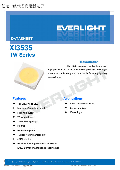
IntroductionThe 3535 package is a lighting gradehigh power LED.It is a compact package with high lumens and efficiency and is suitable for many lighting applications.FeaturesApplications◆Top view white LED ◆ Moisture Sensitivity Level: 1◆High flux output ◆White package ◆Wide viewing angle ◆Pb-free ◆RoHS compliant◆Typical viewing angle: 115°◆ANSI binning◆Reliability testing conforms to IESNA LM80 Lumen maintenance test method◆Omni-directional Bulbs ◆Linear Lighting ◆Panel LightXI35351W Series 亿光一级代理商超毅电子Table of ContentsProduct Nomenclature (3)Absolute Maximum Ratings (4)PN of the XI3535 series: Warm White LEDs (5)PN of the XI3535 series: Neutral White LEDs (6)PN of the XI3535 series: Cool White LEDs (7)Product Binning (8)Mechanical Dimension (16)Pad Configuration (16)Reflow Soldering Characteristics (18)Wavelength Characteristics (19)Typical Electrical Characteristics (19)Typical Relative Luminous Flux V.S. Forward Current (20)Typical Wavelength & Color Shift Characteristics (20)Typical Radiation Patterns (21)Emitter Tape Packaging (22)Emitter Reel Packaging (23)Product Labeling (23)Reliability Data (23)Storage Conditions (24)Revision History (26)Product NomenclatureThe product name is designated as below:XI3535– ABCDEFG–HIJKL–MNOPDesignation:AB = color [1]CD = color bin or CCT bin[1]E = Steps Mcadams binFG = min. luminous flux (lm) or radiation power (mW) performanceHI = forward voltage binJ = internal codeKL = power consumption[2]M = internal codeN = DamO = internal codeP =packaging type[3]Notes1.Table of color offerings:Color CCT range Color Rendering Index GT Cool-White4745~7050K>65KT Cool-White4745~7050K>80PT Cool-White4745~7050K>90HT Cool-White4745~7050K>93Warm-White2580~3710KLM>70Neutral-White3710K-4745KWarm White2580~3710K>80 KMNeutral-White3710K-4745KWarm White2580~3710K>90 PMNeutral-White3710K-4745KWarm White2580~3710K>93 HMNeutral-White3710K-4745K2.Table of power consumptions:Description011W3.Table of packaging types:DescriptionP TapeAbsolute Maximum RatingsMax. DC Forward Current (mA)IF350mA Max. Peak Pulse Current (mA)IPulse720mA Power Dissipation Pd1WThermal Resistance R th15°C/WOperating Temperature Topr-40 ~ +85°CStorage Temperature Tstg-40 ~ +100°CJunction temperature Tj115°C Max. Soldering Temperature T Sol260Notes:1.Maximum forward current for 1W is 350mA (Solder Pad=25°C).2.Duty cycle = 1/10@1KHZMin. LuminousFlux(lm)Typ.LuminousFlux(lm)CCT (K)Wavelength(nm)ForwardVoltage(V)ForwardCurrent(mA)CRI(Min.)XI3535-KM277F9-03201-000P9010027K-1,27K-227K-3,27K-42.95-3.8535080XI3535-KM307F9-03201-000P9010430K-1,30K-230K-3,30K-42.95-3.8535080XI3535-KM357F9-03201-000P9010535K-1,35K-235K-3,35K-42.95-3.8535080XI3535-HM307F8-03201-000P808430K-1,30K-230K-3,30K-42.95-3.8535093Notes:1.Luminous flux measurement tolerance: ±10%.2.The data of luminous flux measured at thermal pad=25°C3.Typical luminous flux or light output performance is operated within the condition guided by this datasheet4.The CRI value is based on the Everlight testing instrument.5.CRI measurement tolerance:±2.Min. LuminousFlux(lm)Typ.LuminousFlux(lm)CCT (K)Wavelength(nm)ForwardVoltage(V)ForwardCurrent(mA)CRI(Min.)XI3535-KM407F9-03201-000P9010740K-1,40K-240K-3,40K-42.95~3.8535080Notes:1.Luminous flux measurement tolerance: ±10%.2.The data of luminous flux measured at thermal pad=25°C3.Typical luminous flux or light output performance is operated within the condition guided by this datasheet4.The CRI value is based on the Everlight testing instrument.5.CRI measurement tolerance:±2.PN of the XI3535 series: Cool White LEDsMin. LuminousFlux(lm)Typ.LuminousFlux(lm)CCT (K)Wavelength(nm)ForwardVoltage(V)ForwardCurrent(mA)CRI(Min.)XI3535-KT507J1-03201-000P10011050K-1,50K-250K-3,50K-42.95-3.8535080XI3535-KT577J1-03201-000P10011157K-1,57K-257K-3,57K-42.95-3.8535080XI3535-KT607J1-03201-000P10010957K-2,57K-365K-1,65K-42.95-3.8535080XI3535-KT657J1-03201-000P10010865K-1,65K-265K-3,65K-42.95-3.8535080XI3535-PT577F9-03201-000P909757K-1,57K-257K-3,57K-42.95-3.8535090Notes:1.Luminous flux measurement tolerance: ±10%.2.The data of luminous flux measured at thermal pad=25°C3.Typical luminous flux or light output performance is operated within the condition guided by this datasheet4.The CRI value is based on the Everlight testing instrument.5.CRI measurement tolerance:±2.Product BinningLuminous Flux Bins14511001102562110120368312013048104130140510135140150613176150160717207160180820238180200E 92327J9200225127331225250233392250275339453275300445524300325552605325350660706350375770807375400880908400425F 990100K9425450White Bin StructureNotes:1.The CCT range of Cool-White varies from 4745K to 7050K.2.The CCT range of Neutral-White varies from 3710K to 4745K.3.The CCT range of Warm-White varies from 2580K to 3710K4.Color coordinates measurement allowance : ±0.015.Color bins are defined at I F =350mA operationCool-White Bin StructureChromaticity specification defined by ANSI亿光一级代理商超毅电子Cool-White Bin Coordinates5000K0.3460.3690.3380.3620.3450.3560.3370.3490.3530.3620.3450.35650K-10.3550.37650K-20.3460.369Reference Range: 4745~5000K Reference Range: 5000~5310K 0.3450.3560.3370.3490.3440.3430.3370.3370.3520.3490.3440.34350K-40.3530.36250K-30.3450.356Reference Range: 4745~5000K Reference Range: 5000~5310K 5700K0.3290.3540.3210.3460.3290.3420.3220.3350.3370.3490.3290.34257K-10.3380.36257K-20.3290.354Reference Range: 5310~5700K Reference Range: 5700~6020K CIE X CIE Y Bin CIE X CIE Y 0.3290.3420.3220.3350.3290.3310.3220.3240.3370.3370.3290.33157K-40.3370.34957K-30.3290.342Reference Range: 5310~5700K Reference Range: 5700~6020K 6000KCIE X CIE Y BinCIE X CIE Y 0.3210.3460.3120.3390.3220.3350.3130.3290.3290.3420.3210.33757K-20.3290.35465K-10.3210.348Reference Range: 5700~6020K Reference Range: 6020~6500K CIE X CIE Y Bin CIE X CIE Y 0.3220.3350.3130.3290.3220.3240.3150.3190.3290.3310.3220.32657K-30.3290.34265K-40.3210.337Reference Range: 5700~6020K Reference Range: 6020~6500K 6500KCIE X CIE Y BinCIE X CIE Y 0.3120.3390.3030.3300.3130.3290.3050.3210.3210.3370.3130.32965K-10.3210.34865K-20.3120.339Reference Range: 6020~6500K Reference Range: 6500~7050K 亿光一级代理商超毅电子0.3130.3290.3050.3210.3150.3190.3070.3110.3220.3260.3150.31965K-40.3210.33765K-30.3130.329Reference Range: 6020~6500KReference Range: 6500~7050KNote:1.Color coordinates measurement allowance : ±0.01.Neutral-White Bin StructureNeutral-White Bin Coordinates4000KCIE X CIE Y BinCIE X CIE Y 0.3870.3960.3740.3870.3830.3800.3700.3730.3950.3880.3830.38040K-10.4010.40440K-20.3870.396Reference Range: 3710~4000K Reference Range: 4000~4260K CIE X CIE Y Bin CIE X CIE Y 0.3830.3800.3700.3730.3780.3650.3670.3580.3900.3720.3780.36540K-40.3950.38840K-30.3830.380Reference Range: 3710~4000K Reference Range: 4000~4260K4500K0.3640.3810.3550.3740.3620.3660.3530.3600.3700.3730.3620.36645K-10.3740.38745K-20.3640.381Reference Range: 4260~4500K Reference Range: 4500~4745K 0.3620.3660.3530.3600.3590.3520.3510.3470.3670.3580.3590.35245K-40.3700.37345K-30.3620.366Reference Range: 4260~4500KReference Range: 4500~4745K Note:1.Color coordinates measurement allowance : ±0.01.Warm-White Bin StructureWarm-White Bin Coordinates2700KCIE X CIE Y BinCIE X CIE Y 0.469 0.429 0.4560.4260.459 0.4100.4470.4080.470 0.413 0.4590.41027K-10.481 0.43227K-20.4690.429Reference Range: 2580~2700K Reference Range: 2700~2870K CIE X CIE Y Bin CIE X CIE Y 0.459 0.410 0.447 0.408 0.448 0.3920.437 0.3890.459 0.394 0.448 0.392 27K-40.470 0.41327K-30.459 0.410Reference Range: 2580~2700K Reference Range: 2700~2870K 3000KCIE X CIE Y BinCIE X CIE Y 0.4430.4210.4300.4170.4350.4030.4220.3990.4470.4080.4350.40330K-10.4560.42630K-20.4430.421Reference Range: 2870~3000K Reference Range: 3000~3220K CIE X CIE Y Bin CIE X CIE Y 0.4350.4030.4220.3990.4260.3850.4150.3810.4370.3890.4260.38530K-40.4470.40830K-30.4350.403Reference Range: 2870~3000K Reference Range: 3000~3220K3500K0.4150.4090.4000.4020.4080.3920.3940.3850.4220.3990.4080.39235K-10.4300.41735K-20.4150.409Reference Range: 3220~3500K Reference Range: 3500~3710K 0.4080.3920.3940.3850.4020.3750.3890.3690.4150.3810.4020.37535K-40.4220.39935K-30.4080.392Reference Range: 3220~3500KReference Range: 3500~3710K Note:1.Color coordinates measurement allowance : ±0.01.Forward Voltage BinsV1 2.95 3.25V2 3.25 3.55V3 3.55 3.85Notes:1.Forward voltage measurement tolerance: ±0.1V.2.Forward voltage bins are defined at I F=350mA operation.Mechanical Dimension..4.2Notes:1.Dimensions are in millimeters.2.Tolerances unless mentioned are ±0.15mm.3.The thermal pad is electrically unity from the Anode and contact pads.4.Do not handle the device by the lens.Incorrect force applied to the lens may lead to the failure of devices.Pad ConfigurationTOP VIEW BOTTOM VIEWPAD FUNCTION1ANODE2CATHODEReflow Soldering CharacteristicsFor Reflow Processa.3535series are suitable for SMT processes.b.Curing of glue in oven must be according to standard operation flow processes.c.Reflow soldering should not be done more than twice.d.In soldering process, stress on the LEDs during heating should be avoided.e.After soldering, do not bend the circuit board.Wavelength CharacteristicsFor Cool-White,Warm-White Relative Spectral Distribution @ Solder Pad Temperature = 254005006007008000.00.20.40.60.81.0Warm-white-CRI>80 Nature-white-CRI>80 Cool-white-CRI>80 Warm-white-CRI>90 Cool-white-CRI>90R e l a t i v e L u m i n o u s I n t e n s t i yWavelength(nm)Typical Electrical CharacteristicsFor Cool-White,Warm-White @ Solder Pad Temperature = 25501001502002503003502.52.62.72.82.93.03.13.23.3F o r w a r d V o l t a g e (V )Forward Current(mA)Typical Relative Luminous Flux V.S. Forward CurrentFor Cool-White ,Warm-White @ Solder Pad Temperature = 250501001502002503003500.00.20.40.60.81.0R e l a t i v e L u m i n o u s I n t e n s i t yForward Current(mA)Typical Wavelength & Color Shift CharacteristicsV.S. Forward CurrentFor Cool-White , Warm-White @ Solder Pad Temperature = 2550100150200250300350200030004000500060007000Cool-White Warm-WhiteC C TForward Current(mA)Forward Current Derating Curve @ Junction Temperature <11520406080100100150200250300350400F o r w a r d C u r r e n t (m A )Soldering Temperature oCTypical Radiation Patterns3535 series:Typical Diagram Characteristics of Radiation for Warm-White andCool-White108090Notes:1.2θ1/2 is the off axis angle from lamp centerline where the luminous intensity is 1/2 of the peak value.2.View angle tolerance is ± 5∘.Emitter Tape Packaging MOQ>2Kpcs, multiple of 400pcs per reel,max 1600pcs MOQ <2Kpcs, multiple of 100pcs per reel,max 1600pcsEmitter Reel Packaging Reel DimensionsNotes:1.Dimensions are in millimeters.2.Tolerances unless mentioned are ±0.1mm.Product LabelingLabel ExplanationCPN: Customer Specification (when required)P/N : Everlight Production NumberQTY: Packing QuantityCAT: Luminous Flux (Brightness) BinHUE: Color BinREF: Forward Voltage BinLOT No: Lot NumberMADE IN TAIWAN: Production PlaceReliability DataReflow Tsol=260 , 10sec 3 timesThermal ShockH 100 20min.'∫ 10sec.'L 10 20min.500,1000 CyclesPower Temperature Cycle H 85 15min.'∫ 5min.'L 40 15min.IF=350mA500,1000 CyclesHigh Temperature/HumidityOperationTa=85 , RH=85%, IF=225mA1000hoursRoom Temperature OperationLifeTa=25 , IF=350mA1000hoursHigh Temperature OperationLife #1Ta=55 , IF=350mA1000hoursHigh Temperature OperationLife #2Ta=85 , IF=225mA1000hoursLow Temperature OperationLifeTa=-40 , IF=350mA1000hoursPulse 30ms ON/2500ms OFF / 30000 CyclesIF=720mA30ms ON/2500ms OFF /30000 CyclesFailure Criteria:1.LEDs are open or shorted2.lm: luminous flux attenuate difference(1000hrs)>50%3.VF: forward voltage difference(1000hrs)>20%Storage Conditions⏹Before the package is opened: The LEDs should be stored at 30°C or less and 50%RH or less after beingshipped from Everlight.The storage life is6 months. If the LEDs are to be stored for more than 6months, they should be stored in a sealed container with a nitrogen atmosphere and moisture absorbent material.⏹After opening the package: The LED's should be stored under 30 or less and 30%RH or less. The LEDshould be used within 168hrs (7days) after opening the package. If unused LEDs remain, they should be stored in moisture proof packages.⏹Before using LEDs: The LEDs should be baked under the following conditions: pre-curing at 60±5 for 24hours.⏹Do not stack assemblies containing Everlight XI3535 LEDs to prevent damage to the optical surface ofLEDs. Forces applied to the optical surface may result in the surface being damaged.Revision HistoryCurrent version: 06.19.2013Issue No:DHE-0002027Version: 10Created by: Betty HongP5,P6,P7New 3000K 4000K 5000K Series.2012-12-07 P7New XI3535-KT657J1-03201-000P2013-02-07 P4Change the Max. Peak Pulse Current2013-03-13 P5,P7Create New CRI>90 spec2013-03-26P21MOQ>2Kpcs, multiple of 400pcs per reelMOQ <2Kpcs, multiple of 100pcs per reel2013-04-09P23Create Reliability Data2013-04-18 P21Create Package Quantity max 1600pcs2013-05-28 P5,P7Added the 4000K and 6000K Color06-19-2013。
亿光光电开关ITR9909
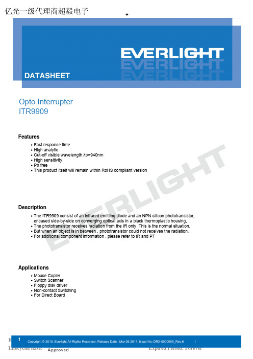
+Opto Interrupter ITR9909Features․Fast response time ․High analytic․Cut-off visible wavelength λp=940nm ․High sensitivity ․Pb free․This product itself will remain within RoHS compliant versionDescription․The ITR9909 consist of an infrared emitting diode and an NPN silicon phototransistor,encased side-by-side on converging optical axis in a black thermoplastic housing,․The phototransistor receives radiation from the IR only .This is the normal situation. ․But when an object is in between , phototransistor could not receives the radiation.․For additional component information , please refer to IR and PTApplications․Mouse Copier ․Switch Scanner ․Floppy disk driver․Non-contact Switching ․For Direct Board亿光一级代理商超毅电子Device Selection GuideDevice No.ChipMaterialsLens ColorIR GaAlAs BluePT Silicon BlackAbsolute Maximum Ratings(Ta=25)Parameter Symbol Ratings Unit Power Dissipation at(or below) 25 Free AirTemperaturePd75mW Reverse Voltage V R5VForward Current I F50mA InputPeak Forward Current (*1)Pulse width100μs,Duty cycle=1%I FP1ACollector Power Dissipation Pd75mWCollector Current I C50mACollector-Emitter Voltage B V CEO30V OutputEmitter-Collector Voltage B V ECO5V Operating Temperature Topr-25~+85 Storage Temperature Tstg-40~+85 Lead Soldering Temperature (*2)(1/16 inch form body for 5 seconds)Tsol260 (*1) tw=100 μsec. , T=10 msec. (*2) t=5 SecElectro-Optical Characteristics (Ta=25)ParameterSymbolMin.Typ.Max.UnitConditions --- 1.21.5I F =20mA--- 1.4 1.85IF=100mA,tp=100 s,tp/T=0.01Forward VoltageVF--- 2.64.0VIF=1A,tp=100 s,tp/T=0.01Reverse Current I R ------10μA V R =5V InputPeak Wavelength λP ---940---nm I F =20mADark C urrentI CEO ------100nA V CE =20V,Ee=0mW/cm2OutputC-E Saturation VoltageV CE (sat)------0.4VI C =2mAEe=1mW/cm 2Collect CurrentI C (ON)200------uA V CE =5V IF=20mA Rise timet r ---15---μsec TransferCharacteristics Fall timet f ---15---μsecV CE =5V,I C =1mA ,R L =1000Ω-201.0-10020107007257507758008258508759009259509751000102510500.00.2R e l a Wavelength (nm)-20402006010080Relative Radiant Intensity vs Forward Current Relative Radiant Intensity vs Angular Displacement110080007000.290010001300110100CRelative Collector Current vs. Ambient Temperature Collector Current vs. Irradiance502585751002Typical Electrical/Optical/Characteristics Curves for ITR Relative Collector Current vs DIistance Between SensorPackage DimensionNote: Tolerances unless dimensions ±0.25mmPacking Quantity Specification1.150PCS/1Bag, 5Bags/1Box2.10Boxes/1CartonNotes1.Above specification may be changed without notice. EVERLIGHT will reserve authority onmaterial change for above specification.2.When using this product, please observe the absolute maximum ratings and the instructionfor using outlined in these specification sheets. EVERLIGHT assumes no responsibility forany damage resulting from use of the product which does not comply with the absolutemaximum ratings and the instructions included in these specification sheets.3.These specification sheets include materials protected under copyright of EVERLIGHT corporation.Please don’t reproduce or cause anyone to reproduce them without EVERLIGHT’s consent.。
MBI5024 Datasheet VB.00-CN
锁功能,可以将串行的输入数据转换成平行输出数据格式。
MBI5024的输入电压范围值为3.3伏特至5伏特,提供16个电流源,可以在每个输出级提供1~45mA定电流量以驱动 LED;且单一颗IC内输出通道的电流差异小于±2%@I OUT =25mA, ±2.5%@I OUT =1mA;多颗IC间的输出电流差异小于±3%;电流随着输出端耐受电压(V DS)变化,被控制在每伏特0.1%;且电流受供给电压(V DD)、环境温度的变化也被控制在1%。
使用者可以经由选用不同阻值的外接电阻器来调整 MBI5024各输出级的电流大小,藉此机制,使用者可精确地控制LED的发光亮度。
MBI5024的设计保证其输出级可耐压17伏特,因此可以在每个输出端串接多个LED。
此外,MBI5024亦提供25MHz 的高时钟频率以满足系统对大量数据传输上的需求。
©聚积科技2010台湾新竹市埔顶路18号6F之4MBI5024GFN输入端。
是高电位时,串行数据会被传入至输出资料会被栓锁住。
轮廓图示使用权声明聚积科技对于产品、文件以及服务保有一切变更、修正、修改、改善、以及终止的权利。
客户在进行产品购买前,建议与聚积科技业务代表联络以取得最新的产品信息。
聚积科技的产品,除非经过聚积合法授权,否则不应使用于医疗或军事行为上,若使用者因此导致任何身体伤害或生命威胁甚至死亡,聚积科技将不负任何损害赔偿责任。
此份文件上所有的文字内容、图片、及商标为聚积科技所属之智慧财产。
除非是先经过聚积合法授权,任何人不得径自使用、修改、重制、公开、改作、散布、发行、公开发表。
如有违反,您应对聚积科技股份有限公司负责损害赔偿责任及其它法律责任。
亿光LED网 PLT131-S-6
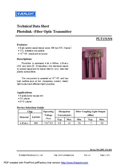
Technical Data SheetPhotolink –Fiber Optic TransmitterPLT131/S/6Features• High speeds signal transmission (6Mbps NRZ Signal ) • TTL interface compatible • +3~+5V single power sourceDescriptionsPhotolink is packaged with a 660nm AlGaAs LED and drive IC .It transforms the electrical signal to optical signal and be transmitted by 1mm diameter plastic optical fiber.The component is operated at +3~+5V and has high performance at low dissipation current, steady light output and efficient light coupling.Applications• Digital audio equipment • CD player • DVD playerDevice Selection GuideChipDissipation Current(mA) Fiber Coupling Light Output(dBm) Material λp(nm)Operating Voltage(Vcc) Typ. Max. Min. Typ. Max. AlGaAs660+3.0~5.05.510-21---15Device NO.:DPL-131-024PLT131/S/6Notes:2.General Tolerance :±0.1mm 2.Vcc3.VinUsing MethodDevice NO.:DPL-131-024PLT131/S/6 Absolute Maximum Ratings( Ta = 25℃)Parameter Symbol Rating Unit Supply Voltage Vcc -0.5 to 7 VDC Input Voltage Vin -0.5 to Vcc+0.5 VStorage Temperature Tstg -40 to 70 ℃Operating Temperature Topr -20 to 70 ℃Soldering Temperature Tsol 260* ℃* Soldering time ≤ 10 s.Electro-Optical CharacteristicsParameter Symbol Conditions MIN. TYP. MAX. Unit Operating Voltage Vcc Low Voltage 2.75 3.00 3.25 VHigh Voltage 4.75 5.00 5.25 V Peak Emission Wavelength λp 640 660 680 nm Transmission Rate NRZ Code DC - 6 Mbps Transmission Distance Using APF* 0.2 - 20 m Fiber Coupling Output Power Pf *1 -21 -18 -15 dBm Dissipation Current Icc *2 3 - 10 mA High Level Input Voltage V IH 2 - - V Low Level Input Voltage V IL- - 0.8 V Low to High Delay Time t pLH*3 - - 180 ns High to Low Delay Time t pHL*3 - - 180 ns Pulse Width Distortion ∆tw *3 -30 - 30 ns *All Plastic Optical Fiber(970/1000um)Device NO.:DPL-131-024PLT131/S/6 Measuring Method*1 Measuring method of optical output coupling fiber*2 Input voltage/power dissipation measuring method*3 Pulse response measuring methodDevice NO.:DPL-131-024。
亿光光藕EL817规格书
Photocoupler-RoHS Compliant EL817 SeriesFeatures: • Current transfer ratio(CTR:MIN.50% at IF =5mA ,VCE =5V) • High isolation voltage between input and output (Viso=5000 V rms ) • Compact dual-in-line package EL817*:1-channel type • Pb free• UL approved (No. E214129) • VDE approved (No. 132249) • SEMKO approved (No. 608400)• NEMKO approved (No. PO6206474/A1) • DEMKO approved (No. 313924-01)• FIMKO approved (No. FI 22807) • CSA approved (No. 1143601) • BSI approved (No. 8592, 8593) • Options available:- Leads with 0.4”(10.16mm) spacing (M Type)- Leads bends for surface mounting (S and S1 Type) - Tape and Reel of Type for SMD(Add”TA” Suffix)Ⅰ - Tape and Reel of Type Ⅱfor SMD(Add”TB” Suffix) - The tape is 16mm and is wound on a 33cm reel• The product itself will remain within RoHS compliant version.DescriptionThe EL817 series contains a infrared emitting diode optically coupled to a phototransistor. It is packaged in a 4-pin DIP package and available in wide-lead spacing and SMD option.Applications• Computer terminals• System appliances, measuring instruments• Registers, copiers, automatic vending machines• Signal transmission between circuits of different potentials and impedancesDevice Selection GuideChip MaterialPart. No.IR PTEL817* GaAs SiliconEL817EL817SEL817MPhotocoupler-RoHS CompliantEL817 SeriesPhotocoupler-RoHS CompliantEL817 SeriesS1 TypeNotes:1.Rank shall be or shall not be marked2.Factory code shall be marked (T: Taiwan / C: China)3.Year date code4.2-digit work week5.All dimensions are in millimeters6.Specifications are subject to change without noticePhotocoupler-RoHS Compliant EL817 SeriesAbsolute Maximum Ratings ( Ta=25°C )Parameter Symbol Rating UnitForward Current I F 50 mAPeak Forward Current*1I FM 1 A Input Reverse VoltageV R 6 V Power Dissipation P 70 mWCollector Power DissipationP C 150 mW Output Collector CurrentI C 50mA Collector-Emitter Voltage V CEO 35 V Emitter-Collector Voltage V ECO 6V Total Power DissipationPtot 200 mW *2Isolation Voltage Viso 5000 V rms Operating TemperatureTopr -55~+110 °C Storage TemperatureTstg -55~+125 °C *3Soldering TemperatureTsol260°C*1Frequency=100 HZ ,10uS Duty*2AC for 1 minute, R.H= 40~ 60%RH-Isolation voltage shall be measured using the following method. (1) Short between anode and cathode on the primary side and between collector, emitter and base on the secondary side.(2) The isolation voltage tester with zero-cross circuit shall be used. (3) The waveform of applied voltage shall be a sine wave*3For 10 secondsPhotocoupler-RoHS Compliant EL817 SeriesElectro-Optical Characteristics (Ta=25°C)Parameter Symbol Min. Typ. Max. Unit ConditionForward V F - 1.2 1.4 V I F =20mA Peak ForwardCurrent V FM 3.0 V I FM =0.5A Reverse Current I R - - 10 uAV R =4VInputTerminal Ct - 30 250 pF V=0,f=1kHz Collector Dark currentI CEO - - 100 nAV CE =20VOutputCollector- Emitter breakdown voltage BV CEO 35 - - V Ic=0.1mACurrent Transfer ratio CTR 50-600 % I F =5mA ,V CE =5VCollector- Emitter saturation voltageV CE(sat) - 0.1 0.2 V I F =20mA ,Ic=1 mAIsolation resistance R ISO 5×10¹⁰ 1011 - ΩDC500V,40~60%R.HFlotation capacitance Cf - 0.6 1.0 pF V=0, f=1MHz Cut-off frequency fc - 80 - kHz V CE =5V, I C =2 mAR L =100Ω, -3dBRise time t r - 4 18 us Transfer CharacteristicsFall timet f - 3 18 usV CE =2VI C =2mA,R L =100ΩPhotocoupler-RoHS CompliantEL817 Series SupplementCurrent Transfer Ratio CTRSub-Model No. Rank mark CTR (%) ConditionEL817* note 1 50 to 600EL817* (L) note2L 50 to 100EL817* (A) A 80 to 160EL817* (B) B 130 to 260 EL817* (C) C 200 to 400 EL817* (D) D 300 to 600 EL817* (AB) A or B 80 to 260 EL817* (BC) B or C 130 to 400 EL817* (CD) C or D 200 to 600 I F = 5 mA V CE = 5 V T a = 25°CNote1. The symbol “ * “ can be none or S or M by different leads form request Note2. The symbol “ ( ) ” can be CTR rankPhotocoupler-RoHS CompliantEL817 Series RELIABILITY PLANz The reliability of products shall be satisfied with items listed below.Confidence level : 90 % , LTPD : 10 %Classification Test Item Description & Condition (Acc.)Sample FailureCriteriaReferenceStandardOperation Life * Ta = 25±3°CIR: If = 50 mAPt: Pc = 130 mW ( Vf=1.4v) , 1000 hrs 0 / 22 MIL-S-750 : 1026MIL-S-883 : 1005JIS C 7021 : B-1High Temperature / High Humidity Reverse Bias (H3TRB) Ta = 85 ±3°C , Humi. = 85 % rhPt: 80% * Vce (max rating) , 1000 hrs0 / 22 JIS C 7021 : B-11High Temperature Reverse Bias (HTRB) Ta = 105 ±3°CPt: 100% * Vce (Max rating) ,1000 hrs0 / 22 JIS C 7021 : B-8Low Temperature Storage Ta = -50 ±3°C , 1000 hrs 0 / 22 JIS C 7021 : B-12High Temperature Storage Ta = 125 ±3°C , 1000 hrs 0 / 22 JIS C 7021 : B-10MIL-S-883 : 1008 Endurance testAuto clave P = 15 PSIG , Ta = 121 °C ,Humi. = 100 % rh , 48 hrs0 / 22 JESD 22-A102-BTemperature Cycling (Air to Air) 125°C ~ - 55 °C30 ~ 30 min , 100 cycles0 / 22 MIL-S-883 :1010JIS C 7021 : A-4Thermal Shock (Liquid to Liquid) 125 ~ - 55°Ct (dwell) = 5 mint (trans.) = 10 sec , 100 cycles0 / 22 MIL-S-202 : 107DMIL-S-750 : 1051MIL-S-883 :1011Solder Resistance Ta = 260 ±3°Ct (dwell) = 10 ±1 sec 0 / 22 MIL-S-750 : 2031JIS C 7021 : A-1Environmental TestSolder Ability Ta = 230 ±3 °Ct (dwell) = 5 ±1 sec 0 / 22CTR shift > 1.2Vf > U* 1.0Ir > U * 1.0Vce(sat) >U*1.0Bvceo < L*1.0Bveco < L*1.0L :LowSpec.LimitU : Up Spec.LimitMIL-S-883 : 2003JIS C 7021 : A-2Photocoupler-RoHS CompliantEL817 Seriesz Packing Quantity1.100 Pcs/ Per Tube2.25 Tubes / Inner Carton3.12 Inner Cartons / Outside Carton3. Outside Carton。
CITIZEN 电子有限公司 LED 包装说明书
AnodeMarking 1Cathode(Tc Measurement Point)Marking 2Marking 1 : Serial No.Marking 2 : 12 05 27 M1YProduct 48pcs/tray3. Precautions for product assembly-When the LED package is attached to the heat sink by M3 screws, please be careful not to apply4. Insulation of the thermal section from the heat sink section of the LED has been confirmedup to 500V. However, for voltages higher than 500V, the customer should confirm the level of insulation Recommended installation screw pitch19.019.07. Lighting at a low currentA minimum current value of lighting of all dice is 25mA.When a minimum current is applied, LED dice may look different in their brightness due tothe individual difference of the LED element, and it is not a failed product.8. Please be aware that this product should not come into contact with any other partsin assembled status.9. Drive circuit- A constant current circuit is recommended as a drive circuit.And when two or more LED packages are connected, the series connectionbetween each package is recommended.- Please design a circuit that prevents any reverse voltage (excess current) from beingapplied to this product instantaneously when the circuit is ON or OFF.10. Heat generation- As this product is designed with consideration of the heat release property of module,a heat release design is required to use this product efficiently.Please ensure that heat generation is not in excess of the absolute maximum rating.(Refer to 4-1 Performance)- Factors responsible for an increase in temperature include heat generation attributed toambient temperature conditions or power dissipation. Thus, drive conditions should betaken into consideration, depending on ambient temperature (Ta).11. Recommended soldering condition (This product is not adaptable to reflow process)- Manual soldering- Soldering shall be implemented using a soldering bit of 40W or less with a temperature350°C or less within 3.5 seconds for one land.(Recommended condition in a case of lead-free solder condition)- No external force shall be applied to resin part during soldering.- Next process of soldering should be carried out after the product has returned to ambient temperature. - For soldering correction- Regarding soldering correction, above conditions shall be used.- Contacts number of soldering bit should be within twice for each terminal as a correction.* Citizen Electronics cannot guarantee if usage exceeds this recommended conditions.Please use it after sufficient verification is carried out on your own risk if necessary.Symbol CITILED12. Eye Safety- The International Electrical Commission (IEC) published in 2006 IEC 62471”2006 Photobiological safety oflamps and lamp systems” which includes LEDs within its scope.When sorting single LEDs according to IEC 62471, most white LEDs can be classified as belonging toeither Exempt Group or Risk Group 1.- However, Optical characteristics of LEDs such as radiant flux, spectrum and light distribution are factors that affect the risk group determination of the LED, and especially a high-power LED,that emits light containing blue wavelengths, may have properties equivalent to those of Risk Group 2.- Great care should be taken when directly viewing an LED that is driven at high current,has multiple uses as a module or when focusing the light with optical instruments,as these actions may greatly increase the hazard to your eyes.- It is recommended to regard the evaluation of stand-alone LED packages as a reference and to evaluate the customer's final product.13. The use of Class 2 power supply is assumed for this product.14. If the product might to be used under the following conditions, the customer must evaluateits approproateness them. This product is not designed for use under the following conditions.in places where the product might:- get wet due to rain- suffer from damage caused by salt.- be exposed to corrosive gas such as Cl, H2S, NH3, SO2, Nox and so on.- be exposed to dust, fluid or oil.Symbol CITILEDDATA SHEET11/11 9. Precautions with regard to product use1. This document is provided for reference purposes only so that CITIZEN ELECTRONICS'products are used as intended. CITIZEN ELECTRONICS neither makes warranties orrepresentations with respect to the accuracy or completeness of the information containedin this document nor grants any license to any intellectual property rights or any otherrights of CITIZEN ELECTRONICS or any third party with respect to the informationin this document.2. All information included in this document such as product data, diagrams, charts,is current as of the date this document is issued.Such information, however, is subject to change without any prior notice.Before purchasing or using any CITIZEN ELECTRONICS' products listed in this document,please confirm the latest product information with a CITIZEN ELECTRONICS' sales office,and formal specifications must be exchanged and signed by both parties prior to mass production.3. CITIZEN ELECTRONICS has used reasonable care in compiling the informationincluded in this document,but CITIZEN ELECTRONICS assumes no liability whatsoever for any damages incurred asa result of errors or omissions in the information included in this document.4. Absent a written signed agreement, except as provided in the relevant terms and conditions ofsale for product, and to the maximum extent allowable by law, CITIZEN ELECTRONICSassumes no liability whatsoever, including without limitation, indirect, consequential, special,or incidental damages or loss, including without limitation, loss of profits, loss of opportunities,business interruption and loss of data, and disclaims any and all express or implied warrantiesand conditions related to sale, use of product, or information, including warrantiesor conditions of merchantability, fitness for a particular purpose, accuracy of information,or no infringement.5. Though CITIZEN ELECTRONICS works continually to improve products' quality and reliability,products can malfunction or fail. Customers are responsible for complying with safety standardsand for providing adequate designs and safeguards to minimize risk and avoid situationsin which a malfunction or failure of a product could cause loss of human life,bodily injury or damage to property, including data loss or corruption.In addition, customers are also responsible for determining the appropriateness ofuse of any information contained in this document such as application cases not only withevaluating by their own but also by the entire system.CITIZEN ELECTRONICS assumes no liability for customers' product design or applications.6. Please contact CITIZEN ELECTRONICS' sales office if you have any questions regardingthe information contained in this document, or if you have any other inquiries.CITIZEN Micro HumanTech is a registered trademark of Citizen Holding Co., Japan.CITILED is a registered trademark of CITIZEN ELECTRONICS CO., LTD. JapanSymbol CITILEDName CLL030-1205A1-273M1A2CITIZEN ELECTRONICS CO.,LTD. JAPANRef.CE-P1527 10/11。
厉光电子 Everlight 0603 包装红外 LED 技术数据表说明书
Technical Data Sheet0603 Package Infrared LEDIR19-315C/TR8 Array Features․Peak wavelength λp=940nm․Package in 8mm tape on 7” diameter reel․Compatible with infrared and vapor phase reflow solder process.․Pb free․The product itself will remain within RoHS compliant version.․Compliance with EU REACH.․Compliance Halogen Free .(Br <900 ppm ,Cl <900 ppm , Br+Cl < 1500 ppm)Description․IR19-315C/TR8 is an infrared emitting diode in miniature SMD package which is molded in a water clear epoxy The device is spectrally matched with silicon photodiode and phototransistor. Applications․PCB mounted infrared sensor․Infrared remote control units with high power requirement․Scanner․Infrared applied systemDevice Selection GuideAbsolute Maximum Ratings (Ta=25℃)Notes: *1:Soldering time≦5 seconds.Electro-Optical Characteristics (Ta=25℃)RankCondition:I F=20mAPrecautions For Use1.Over-current-proofCustomer must apply resistors for protection , otherwise slight voltage shift will cause bigcurrent change ( Burn out will happen ).2.Storage2.1 Do not open moisture proof bag before the products are ready to use.2.2 Before opening the package, the LEDs should be kept at 30℃or less and 90%RH or less.2.3 The LEDs should be used within a year.2.4 After opening the package, the LEDs should be kept at 30℃or less and 60%RH or less.2.5 The LEDs should be used within 168 hours (7 days) after opening the package2.6 If the moisture absorbent material (silica gel) has faded away or the LEDs have exceeded the storagetime, baking treatment should be performed using the following conditions.Baking treatment : 60±5℃for Min. 24 hours.3.Soldering Condition3.1 Pb-free solder temperature profile3.2 Reflow soldering should not be done more than two times.3.3 When soldering, do not put stress on the LEDs during heating.3.4 After soldering, do not warp the circuit board.4.Soldering IronEach terminal is to go to the tip of soldering iron temperature less than 350℃ for 3 seconds within once in less than the soldering iron capacity 25W. Leave two seconds and more intervals, and do soldering of each terminal. Be careful because the damage of the product is often started at the time of the hand solder.5.RepairingRepair should not be done after the LEDs have been soldered. When repairing is unavoidable, a double-head soldering iron should be used (as below figure). It should be confirmed beforehand whether the characteristics of the LEDs will or will not be damaged by repairing.Note: The tolerances unless mentioned is ±0.1mm ,Unit = mmCAT: RanksHUE: Peak Wavelength REF: ReferenceLOT No: Lot NumberMADE IN TAIWAN: Production PlaceDISCLAIMER1. EVERLIGHT reserves the right(s) on the adjustment of product material mix for the specification.2. The product meets EVERLIGHT published specification for a period of twelve (12) months from date of shipment.3. The graphs shown in this datasheet are representing typical data only and do not show guaranteed values.4. When using this product, please observe the absolute maximum ratings and the instructions for using outlined in these specification sheets. EVERLIGHT assumes no responsibility for any damage resulting from the use of the product which does not comply with the absolute maximum ratings and the instructions included in these specification sheets.5. These specification sheets include materials protected under copyright of EVERLIGHT. Reproduction in any form is prohibited without obtaining EVERLIGHT’s prior consent.6. This product is not intended to be used for military, aircraft, automotive, medical, life sustaining or life saving applications or any other application which can result in human injury or death. Please contact authorized Everlight sales agent for special application request.XXXXXXXXXXXXXXXXXXXX-XXXXXXXXXX-XXXXXXXXXX XXXXXXXXXX XXXXXXXXXXBTPYYMMDDXXXXXMADE IN XXXXXXMSL-X。
亿光红外线接收头IRM-H638T-TR2
Technical Data SheetInfrared Remote-control Receiver ModuleIRM-H6XXT/TR2 Features‧High shielding against electric field disturbance.‧Circular lens to improve the receive characteristic.‧Line-up for various center carrier frequencies.‧Low voltage and low power consumption.‧High immunity against ambient light.‧Photodiode with integrated circuit.‧TTL and CMOS compatibility.‧Top-received SMD.‧Suitable burst length ≧10 pulses/burst.‧This product itself will remain within RoHS compliant version.‧Pb free.‧External dimensions 5(L)*7(W)*4(H)mm.DescriptionsThe device is a miniature SMD type infrared remotecontrol system receiver that has been developed anddesigned by utilizing the most updated IC technology. ThePIN diode and preamplifier are assembled on lead frame,the epoxy package is designed as an IR filter. Thedemodulated output signal can directly be decoded by amicroprocessor.Applications1. Light detecting portion of remote control․AV instruments such as Audio, TV, VCR, CD, MD, etc.․Home appliances such as Air-conditioner, Fan , etc.․The other equipments with wireless remote control.․CATV set top boxes․Multi-media EquipmentDevice Selection GuidePART MATERIAL COLORChip Silicon ---Package Epoxy BlackIRM-H6XXT/TR2 Absolute Maximum Ratings (Ta=25℃)Parameter Symbol Rating Unit NoticeSupply Voltage Vcc 0~6 V Operating Temperature Topr -25 ~ +85 ℃Storage Temperature Tstg -40 ~ +85 ℃Recommended Operating ConditionSupply Voltage Rating: Vcc 2.7V to 5.5VElectro-Optical Characteristics (Ta=25℃, and Vcc=3.0V)Parameter SymbolMIN.TYP.MAX.UnitCondition Supply Current Icc --- --- 1.2 mA No signal input Peak Wavelength λp--- 940 --- nmL08 --- ---Reception DistanceL45 5 --- ---mHalf Angle(Horizontal) Θh--- 45 --- deg At the ray axis*1Half Angle(Vertical) Θv--- 45 --- degHigh Level Pulse Width T H400 --- 800 μs Low Level Pulse Width T L400 --- 800 μs At the ray axis*2High Level Output Voltage V H 2.7 --- --- V Low Level Output Voltage V L--- 0.2 0.5 V Notes:*1:The ray receiving surface at a vertex and relation to the ray axis in the range of θ= 0° and θ=45°.*2:A range from 30cm to the arrival distance. Average value of 50 pulses.IRM-H6XXT/TR2 The Notice of Application:Transmission remote control signal consist of four parts: Encode Part, IR Transmitter Source, IRM device, Decode Part1. When IRM-H6XXT code select frequency, it need to well understand the center system ofencode part.2. Strong or weak light of IR Transmitter can affect distance of transmission.3. Minimum Burst Length T burst (number of pulses per burst) : 10 cycles4. It needs to ensure the translation range of decode part if it is applied to the pulse-width range. If the above items hardly assure of its application, it’ll cause NG(no good) message from the edge of signal.Note: This model might not work well with RCA code.Test Method:The specified electro-optical characteristics is satisfied under the followingConditions at the controllable distance.c Measurement placeA place that is nothing of extreme light reflected in the room.d External lightProject the light of ordinary white fluorescent lamps which are not highFrequency lamps and must be less then 10 Lux at the module surface.(Ee≦10Lux)e Standard transmitterIRM-H6XXT/TR2Application Circuit:RC Filter should be connected closely between Vcc pin and GND pin.IRM-H6XXT/TR2Fig.-8 Fig.-9 Relative Transmission Distance vs.Fig.-9 Arrival Distance vs. Ambient TemperatureCenter Carrier FrequencyReliability Test Item And ConditionThe reliability of products shall be satisfied with items listed below.Confidence level:90%LTPD:10%Reflow Terms: JEDEC Level 4 SpecificationDrying; Temp.:125℃ 24hrs Æ Moisture 30℃/ 60% RH 96hrs Æ Reflow Temp.: 260℃±5℃10sec, 3 timesNote:1. Not sooner than 15 minutes and not longer than 4 hours after removal from thetemperature/humidity chamber.2. The time between reflow shall be 5 minutes minimum and 60 minutes maximum.Recommended method of storageDry box storage is recommended as soon as the aluminum bag has been opened prevent moisture absorption. The following conditions should be observed, if dry boxes are not available:z Storage temperature 10℃ to 30℃z Storage humidity ≦60%RH max.After more than 72 hours under these conditions moisture content will be too high for Reflow soldering:In case of moisture absorption, the devices will recover to former condition by drying under the following condition:192 hours at 40℃+5℃/-0℃and 5%RH (dry air / nitrogen) or96 hours at 60℃+5℃and < 5%RH for all device containers or24 hours at 125℃+5℃not suitable for reel or tubes.ESD PrecautionProper storage and handing procedures should be followed to prevent ESD damage tothe devices especially when they are removed from the Anti-static bag. Electro-Static Sensitive Devices warning labels are on the packing.Recommended Solder Profile(1) Reflow soldering should not be done more than two times.(2) When soldering, do not put stress on the IRM-H6XXT/TR2 Series devices during heating.(3) After soldering, do not warp the circuit board.Soldering IronEach terminal is to go to the tip of soldering iron temperature less than 350℃ for 3 seconds within once in less than the soldering iron capacity 25W. Leave two seconds and more intervals, and do soldering of each terminal. Be careful because the damage of the product is often started at the time of the hand solder.RepairingRepair should not be done after the Devices have been soldered. When repairing is unavoidable, a double-head soldering iron should be used (as below figure). It should be confirmedBar Code Label亿光一级代理商超毅电子EVERLIGHT ELECTRONICS CO.,LTD.IRM-H6XXT/TR2Label Form SpecificationCPN: Customer’s Production Number P/N : Production Number QTY: Packing Quantity CAT: None HUE: None REF: Reference LOT No: Lot Number MADE IN CHINA: Production PlacePbRoHSIRM-H6XXT/TR2Notes1. Above specification may be changed without notice. EVERLIGHT will reserve authority on material change for above specification. 2. When using this product, please observe the absolute maximum ratings and the instructions for using outlined in these specification sheets. EVERLIGHT assumes no responsibility for any damage resulting from use of the product which does not comply with the absolute maximum ratings and the instructions included in these specification sheets. 3. These specification sheets include materials protected under copyright of EVERLIGHT corporation. Please don’t reproduce or cause anyone to reproduce them without EVERLIGHT’s consent.EVERLIGHT ELECTRONICS CO., LTD. Office: No 25, Lane 76, Sec 3, Chung Yang Rd, Tucheng, Taipei 236, Taiwan, R.O.CTel: 886-2-2267-2000, 2267-9936 Fax: 886-2267-6244, 2267-6189, 2267-6306 http:\\Everlight Electronics Co., Ltd. Device No:DMO-0000008http:\\ Prepared date:09 -26-2007Rev1Page: 11 of9Prepared by:IBU_NPID2。
- 1、下载文档前请自行甄别文档内容的完整性,平台不提供额外的编辑、内容补充、找答案等附加服务。
- 2、"仅部分预览"的文档,不可在线预览部分如存在完整性等问题,可反馈申请退款(可完整预览的文档不适用该条件!)。
- 3、如文档侵犯您的权益,请联系客服反馈,我们会尽快为您处理(人工客服工作时间:9:00-18:30)。
Technical Data Sheet
0603 Package Chip LED (0.4mm Height)
19-217/R6C-P1Q2/3T Features
․Package in 8mm tape on 7〞diameter reel.
․Compatible with automatic placement equipment.
․Compatible with infrared and vapor phase reflow
solder process.
․Mono-color type.
․Pb-free.
․The product itself will remain within RoHS complaint Version.
Descriptions
․The 19-217 SMD LED is much smaller than lead
frame type components, thus enable smaller
board size, higher packing density, reduced
storage space and finally smaller equipment to be
obtained.
․Besides, lightweight makes them ideal for
miniature applications. etc.
Applications
․Backlighting in dashboard and switch.
․Telecommunication: indicator and backlighting in
telephone and fax.
․Flat backlight for LCD, switch and symbol.
․General use.
Device Selection Guide
19-217/R6C-P1Q2/3T Package Outline Dimensions
Note: The tolerances unless mentioned is ±0.1mm ,Unit = mm
19-217/R6C-P1Q2/3T
Notes: Tolerance of Luminous Intensity ±11%
19-217/R6C-P1Q2/3T Bin Range Of Luminous Intensity
Notes: Tolerance of Luminous Intensity ±11%.
19-217/R6C-P1Q2/3T Typical Electro-Optical Characteristics Curves
19-217/R6C-P1Q2/3T Label explanation Array CAT:Luminous Intensity Rank
HUE: Dom. Wavelength Rank
REF:Forward Voltage Rank
Reel Dimensions
Note: The tolerances unless mentioned is ±0.1mm ,Unit = mm
19-217/R6C-P1Q2/3T Carrier Tape Dimensions: Loaded quantity 3000 PCS per reel
Note: The tolerances unless mentioned is ±0.1mm ,Unit = mm
19-217/R6C-P1Q2/3T Reliability Test Items And Conditions
The reliability of products shall be satisfied with items listed below.
Confidence level:90%
LTPD:10%
19-217/R6C-P1Q2/3T Precautions For Use
1. Over-current-proof
Customer must apply resistors for protection , otherwise slight voltage shift will cause big
current change ( Burn out will happen ).
2. Storage
2.1 Do not open moisture proof bag before the products are ready to use.
2.2 Before opening the package: The LEDs should be kept at 30℃or less and 90%RH or less.
2.3 After opening the package: The LED's floor life is 1 year under 30℃or less and 60% RH or less.
If unused LEDs remain, it should be stored in moisture proof packages.
2.4 If the moisture absorbent material (silica gel) has faded away or the LEDs have exceeded the
storage time, baking treatment should be performed using the following conditions.
Baking treatment : 60±5℃for 24 hours.
3. Soldering Condition
3.1 Pb-free solder temperature profile
3.2 Reflow soldering should not be done more than two times.
3.3 When soldering, do not put stress on the LEDs during heating.
3.4 After soldering, do not warp the circuit board.
19-217/R6C-P1Q2/3T 4.Soldering Iron
Each terminal is to go to the tip of soldering iron temperature less than 350℃for 3 seconds within once in less than the soldering iron capacity 25W. Leave two seconds and more intervals, and do soldering of each terminal. Be careful because the damage of the product is often started at the time of the hand solder.
5.Repairing
Repair should not be done after the LEDs have been soldered. When repairing is unavoidable, a double-head soldering iron should be used (as below figure). It should be confirmed beforehand whether the characteristics of the LEDs will or will not be damaged by repairing.。