(完整版)fpga跨时钟域设计
fpga数字时钟课程设计
fpga数字时钟课程设计FPGA数字时钟课程设计随着科技的不断发展,数字时钟已经成为现代人生活中必不可少的物品。
数字时钟的准确性和便捷性吸引了越来越多的人使用。
而现在,我们可以通过FPGA数字时钟课程设计来实现一个高精度的数字时钟。
FPGA(Field Programmable Gate Array)是一种可编程逻辑器件,可以通过编程实现各种不同的功能。
数字时钟的实现也可以通过FPGA来完成。
在FPGA数字时钟课程设计中,我们需要先确定时钟的基础部分。
时钟的基础部分由时钟信号产生器、时钟分频器、时钟计数器和时钟显示器组成。
时钟信号产生器需要产生一个稳定的时钟信号,以供后续的计数器和分频器使用。
我们可以通过FPGA中的时钟模块来产生一个稳定的时钟信号。
接下来,时钟分频器需要将时钟信号分频,使得计数器可以进行精确的计数。
分频器的分频系数可以通过FPGA中的数码开关进行设置。
然后,时钟计数器需要根据分频器的设定进行精确的计数。
计数器的计数值可以通过FPGA中的计数器模块进行设置。
时钟显示器需要将计数器的计数值进行显示。
我们可以通过FPGA 中的数码管模块来实现时钟的显示功能。
除了基础部分,我们还可以通过添加更多的功能来完善数字时钟。
例如,我们可以添加闹钟功能、日期显示功能等,以增加数字时钟的实用性。
在FPGA数字时钟课程设计中,我们可以使用VHDL(VHSIC Hardware Description Language)语言进行编程。
VHDL是一种硬件描述语言,可以用于FPGA和ASIC的设计。
通过编写VHDL 程序,我们可以实现数字时钟的各种功能。
FPGA数字时钟课程设计是一个非常有趣和实用的课程项目。
通过这个项目,我们可以深入了解数字时钟的工作原理,熟悉FPGA的编程方法,同时也可以锻炼自己的编程能力。
FPGA跨时钟域亚稳态研究
有时序要求 。 “ 建立时 间” ( e u 和 复杂 化 ,只 要系 统 中存 在跨 时钟 产 生亚 稳 态 ,此 时 触发 器 输 出端 Q Stp
tm )是指在时钟沿到来之前 ,触发 域 ,亚稳态就是无法避免的,因此设 在有 效 时钟 沿之后 较长 时间处于 不 ie
器输 入信号 必须保 持稳 定 的时间 。 计 的电路首先要减少亚稳态导致错误 确定状态 ,在这段时间 内Q 端产生毛 “ 保持时间 ” (o d t m )则是指 的发生,其次要使系统对产生的错误 刺并 不断振 荡 ,最 终 固定在某一 个 H l ie
即所有时钟寄存器 的时钟共享一个时 的建立 时间T U S )之 前保 持 稳 定 ,
2 2亚稳态分析 . 跨 时钟异 步输入信 号可 以在任
并且 持续 到时钟沿 之后 的某段 时 间
( 寄存 器 的保 持 时间T )之后 才 能 何 时间 点翻转 ,它与下 级 同步采样 h
辑器件 内采用多个时钟,且核心模块 改变 。寄存器 的输 入反 映到输 出则 信 号没有 必然联 系 。此 外 ,在 数据
在 时钟 沿之 后 ,信 号必 须保 持稳定 不敏感。前者要靠 同步来实现 ,而后 值 ,这 个值 不一定 等于 原来数据 输 的 时间 。这 些指标 通常 比较保 守 , 度 )环 境下 时序各 有差异 的情 况 。 如果一个设计满足 了这些 时序要求 , 则 触发器 出现 错误 的可是一 个不 e i
F G 设计 中,要 减少亚稳 态导 正确 定 的稳 态值 。也就 是说这 种处 PA
定状态 ,就会导致系统混乱 。
致 的错误 并使系 统对产 生 的错 误不 理方 法不 能排 除采 样错 误 的产 生 。
亚 稳态 的危害 主要是 破坏 系统 敏感 ,就要 正确 定义和处 理F G 内 P A 这 时就要 求所 设计 的系 统对采 样错
cpu与fpga跨时钟域数据交换的实现问题

munitis#1楼主:cpu与fpga跨时钟域数据交换的实现问题[精华]ARM与fpga(cyclone)之间进行数据传输,这应该属于跨时钟域的范畴,CPU与fpga之间采用三总线的方式进行连接,而CPU连接fpga的数据线、地址线、控制线进入fpga内部就属于异步信号了,该如何考虑呢?我看过一些关于跨时钟域的文献,上面说对于数据交换,实现方法有握手和fifo两种,我想,双口RAM是不是也算一种?另外,我看跨时钟域数据交换,都涉及到两侧的时钟信号,而对于CPU的三总线,并没有输出什么时钟信号,时钟输出是不是必须的呢?问题比较多,不知道说明白没有,请指教一二,谢谢了!riple #2这个问题,基本上很难。
开个玩笑,原理上简单,实现起来有许多要注意的地方,但是不难。
一个提示:从你使用的ARM芯片数据手册的接口时序图入手。
FPGA中的处理方法是可以改的,而接口时序是一定要遵守的。
泛泛而谈很难,把你的芯片接口时序图贴上来吧,主要是寄存器读、写时序,如果用到DMA的话,应该还有DMA读写的时序图。
munitis #3上面是ARM读写外设的时序图,时钟是CPU的,和fpga的内部时钟是两个时钟域,既需要有ARM写入给fpga 内部的寄存器,又需要有ARM读出fpga内部的值,该如何解决跨时钟域的问题呢?munitis #4ARM与fpga的接口是标准的总线型接口,包括DATA,CS,ADDR,RD,WR,这些信号由CPU的时钟控制,对于FPGA来说是异步信号,在进入FPGA内部是不是需要先进行同步,我看过一些文献,这种总线型的跨时钟域,是不能用多个同步器进行同步的,采用的方法有握手信号和FIFO,是不是这样的呢?riple #5我们一步一步来,先实现基本功能,然后优化性能。
第一、我觉得处理这样的接口,采用异步方式比较好。
因为同步接口对FPGA外部电路和内部配置的要求都比较高。
异步接口只要给出充分的时间,外部电路不存在信号完整性问题就很好解决。
FPGA与SoC芯片设计中五步法CDC跨时钟域检查方法学

Advanced Verification White Paper Five Steps to QualityCDC VerificationPing Yeung Ph.D.Mentor GraphicsCDC synchronizers are used to reduce the probability of metastable signals. Taking unpredictable metastable sig-nals and creating predictable behavior, they prevent metastable values from reaching the receiving clock domain.Metastability EffectsEven when proper CDC synchronizers are used for all clock-domain crossings and all CDC protocols are cor-rectly implemented, metastability inevitably leads to unpredictable cycle-level timing [4, 5]. Traditional RTL simulation does not model metastability, therefore, it cannot be used to find functional problems that may arise when metastability manifests in hardware. We are going to show two scenarios in which the cycle-level timing of RTL simulation differs from the cycle-level timing of the actual hardware in the presence of metastability.In Figure 3, the incoming CDC signal, cdc_d , violates the register setup time. Although it is sampled correctly in RTL simulation, the register is metastable and the output settles to 0. As a result, the hardware transition is delayed by one cycle.Figure 2: A two-register CDC synchronizer.Figure 4: Hold time violation: hardware transition is advanced by one cycle.Figure 3: Setup time violation: hardware transition isdelayed by one cycle.In Figure 4, the incoming CDC signal, cdc_d, violates the register hold time. In RTL simulation, it is not sam-pled until the next cycle. However, the register is metastable and the output settles to 1. As a result, the hardware transitions one cycle before simulation.CDC VerificationMany designers know that metastability can be controlled using synchronizers on CDC signals. The most com-mon solution is to use synchronizers made up of two D flip-flops (2-DFF), or more, in sequence to dramatically increase the mean time between failure (MTBF) of the crossings. It is important to point out that simply ensur-ing the presence of synchronizers on the appropriate signals, while necessary, is not nearly sufficient. There are three different aspects of CDC verification that must be carefully addressed:•Structural verification. Each synchronizer must have the correct structure for the type of signal being sent across clock domains. For example, a 2-DFF synchronizer is usually the best solution for single-bit signals but should not be used for multi-bit signals unless they are gray-coded to ensure that only one bit changes at a time [1, 2]. Multi-bit signals may be synchronized across domains using a separate control signal, an asynchronous FIFO, or other methods. Also, there should be no combinational logic inside or before a synchronizer.•Protocol verification. Each synchronizer must follow a set of rules, called a transfer protocol, to ensure that the CDC signal is properly transferred across clock domains. For example, even the simplest 2-DFF synchronizer requires that the transmitting signal be held stable long enough to guarantee that it is captured in the receiving domain. This may not occur if the transmitting clock is faster than the receiving clock. Synchronization structures for multi-bit signals require more complex protocol checks [2, 3]. When CDC transfer protocols are violated, an error may not occur in simulation but will eventually occur in real hardware.•Metastability verification. Problems associated with the reconvergence of CDC signals must be avoided. Reconvergence occurs when multiple signals are synchronized separately from one clock domain to another and then used by the same logic in the receiving domain (Figure 5). If that logic assumes a timing relationship between the signals, the design is not tolerant of metasta-Figure 5: Reconvergence of CDC signals.running CDC verification at the chip-level is not idealas there are too many behavioral models. For this reason, designs with the RTL representation arebest suited for CDC verification. All multiple-bit regis-ters and buses can be identified explicitly. As CDCrequirements for data and control signals are different,they can be analyzed separately. Conversely, with a gate-level representation, all buses have been synthesized intosingle-bit wires. It is impossible to distinguish data fromcontrol signals. Thus, only a subset of the CDC schemeis applicable.In addition, knowledge of the internal structure of thedesign is essential for successful CDC verification.Performing CDC analysis on third-party IP blocks orlegacy designs are not very beneficial. Without designknowledge, you may not be able to confirm the bugs orfilter violations. You need access to the original design-er; knowledge of the design is essential to understandthe results.Document CDC requirements This step is important. It has the biggest impact on the quality of the result. You need to ensure that your CDC verification will be aware of all relevant design characteristics, clock relationships, and the external environ-ment. Although a set of CDC rules have been defined already in the tool, with this additional information, extra design rules and filters will be activated. As a result, the results will be more accurate and thorough. You should define the operational modes of the design, outline the clock structures, document the domains for interface sig-nals, and determine the acceptable or unacceptable synchronization rules.•Define operational modes . Some users may be interested in verifying that all registers are driven by only the test clock when the design is in scan mode. However, in general, we want to perform CDC verification when the design is in normal operation. You should disable the non-functional modes (i.e., test, BIST, JTAG , etc.)and define the meaningful operational modes and configurations for the tool (Figure 8). In many cases, some parts of a design can be put into sleep or powered-down mode. The combinations can be countless. Hence, it is important to focus CDC verification on the important combinations.•Outline clock structures . For a multiple-clock design, the primary clocks, the clock distribution structure, and the internal clock generators, dividers, and clock gating schemes are important and should be documented. The 0-In CDC tool [7] can understand these structures and extract the clock tree information automatically. It is useful to verify the original design intent with the extracted clock structures. Only crossings between asynchronous clocks should be analyzed, and there may be clock gating conditions that need to be set up properly. As the number of CDC paths Figure 7: Blocks suitable for running CDC verification are A, C, and D.Figure 8: Define meaningful modes for CDC verification.is proportional to the number of clock domains, it is much more efficient to limit analysis to the relevant clock domains only.•Document interface signals.CDC verification will not check an interface signal if it does not know which clock domain it is coming from or fanning out to. You should group signals for each functional interface and clock domain and explicitly identify any input signals that are asynchronous to all clock domains. The tool will then determine whether input signals require synchronization before use. Asynchronous and synchro-nous reset signals should be labeled separately. The synchronization schemes used for reset signals are dif-ferent from normal interface signals.•Define synchronization rules.Some companies require all CDC signals to be synchronized with a particular CDC scheme (for instance, 3-level DFFs) or with a custom synchronization cell. The 0-In CDC tool [7] rec-ognizes many CDC schemes. It is important to review those schemes first. Then you can categorize the legal or illegal synchronization schemes, turn off the unused schemes and capture the characteristics of the syn-chronization cells or modules.Some detail-oriented designers will specify the clock domain information and capture the CDC paths in the design document. This is a practice we encourage. With this information, you can pay special attention to the specified CDC paths to ensure they are well covered.Formalize known exceptionsIt is not unusual that a simple CDC error will generate a lot of violations, especially when the CDC signal fans out to a large number of asynchronous domains. Hence, we want to identify upfront all registers that can be con-sidered stable and do not require synchronization. This is especially true for configuration registers, status regis-ters, or control registers that are programmed by software before the design enters into normal operation. Usually this information is in the design specification. Often these control registers all reside within a single module or follow a common naming scheme. It is useful to leverage this information for CDC verification.In addition to registers, some of the interface or internal signals are known to be stable during normal opera-tion; for example, the internally generated reset signals, the power-down signals, the chip select, and functional enable and disable signals. These are all useful in improving the efficacy of CDC verification. Finally, in previ-ous revisions of the chip, there may be known CDC bugs and issues found using manual or gate-level method-ologies.. These are painful lessons which should be captured in the verification plan. During CDC verification, you should ensure that those CDC paths are analyzed and that all problems were fixed correctly.Define coverage goalsBased on our experience, CDC paths are poorly verified by traditional functional verification because, in a functional simulation environment, the clock periods are defined to be constants, the clock skews and relation-ships are fixed, and the clock signals are well-behaved without any buffer or propagation delay. To ensure metastability effects on CDC paths are better verified, companies use various ad-hoc approaches. Some ran-domly reduce or prolong the clock periods. Some randomly change the skews and relationships among multiple asynchronous clocks.Regardless of the technique used, when verifying CDC transfer protocols in simulation, it is important to moni-tor protocol coverage to make sure the CDC paths are adequately verified. This can be done by using a checker from an assertion library [9, 10, 11] to capture the semantics of the protocol. Checkers collect coverage infor-mation to ensure that each CDC protocol is fully exercised. Insufficient coverage means that the design may contain undiscovered bugs.CDC Handshake:- Assertion:i.multiple requests violationii.acknowledge without request violationiii.request drop violationiv.acknowledge timeout violation- Coverage:i.#request assertedii.#acknowledge assertedCDC FIFO:- Assertion:i.FIFO overflow violationii.FIFO underflow violationiii.Simultaneous push and pop violation- Coverage:i.#push assertedii.#pop assertediii.maximum FIFO entryYou start by itemizing the protocols used in the CDC paths, ordering them from most important to least, and identifying the protocols that require coverage. For each CDC protocol, you will determine the assertion and coverage items, as in the code shown above. To measure how well your simulation is verifying the metastability effects, you should also monitor the alignments of the RX and the TX clocks.Select a verification strategyYou may choose to perform exhaustive verification on each individual block or use a hierarchical approach on the entire top-level of a chip. The top-level represents the highest functional hierarchy of the design, excluding the pad ring, the test logic, the power controls, etc. You may be looking for a known bug or hunting for a prob-lem that has appeared in the lab. The strategies you choose will determine how to run your CDC analysis tools. Based on our experience, there are four common strategies•Block-level verification.During block-level design, static analysis of the CDC structures should be run before checking in the RTL code. This ensures strict compliance with CDC schemes. If issues are discov-ered, they can be identified and debugged quickly at this level. The generated CDC protocol monitors can also be used with block-level functional verification methodologies, such as formal verification [8] and simulation. These ensure that CDC protocols are followed without any data loss.•Top-level verification. During top-level integration, static analysis of the CDC structures should be re-run to check the new CDC signals created when multiple blocks are integrated together. The number of CDC signals goes up exponentially at the top-level. Hence, it is important to follow the five-step planning processdescribed above. For large and complex designs, especially ones with a lot of IP modules, a hierarchical veri-fication approach can be used. The generated CDC protocol monitors should be included in the regression for system-level functional verification.•Bug hunting and triage. This is performed to identify known or suspected CDC issues in the design. It is important to distinguish timing from CDC issues. Timing issues tend to cause the chip to fail consistently. By changing the frequencies of the clocks or of some of the signals, the problems may disappear permanently. On the other hand, as metastability is unpredictable, CDC problems will cause the chip to fail randomly. Based on our experience, it is extremely difficult to look for CDC issues at the system or chip level. There are just too many potential candidates. Hence, the first task is to narrow down the problem to the block or subsystem level.You should focus on blocks with asynchronous clock domains. Blocks with CDC reconvergence are especially suspicious. The random delays from different CDC paths may cause the data to be sampled incorrectly or cor-rupted completely. Once the candidate blocks are identified, the block-level verification strategy can be applied.•Targeting coverage.This can be an extension of the block-level or top-level verification strategy. The goal is to ensure that all CDC protocols have been fully exercised and that the metastability effects are fully verified on all CDC paths. The coverage on the CDC protocols monitors should be examined and additional tests created to fill any coverage holes. Once the bug rate of system-level regression has stabilized, metastability can be injected into simulation. Metastability effects will change the timing of the CDC paths. If the block is not designed to handle the random delays of the CDC paths, it may fail functionally. To make debugging easier, it is better to start with a representative subset of the regression.In the next two sections, we will elaborate on the two most commonly used strategies: block-level andtop-level verification.•Correctly implemented synchronizers•Missing and incorrectly implemented synchronizers•Complex synchronizers that require protocol verification•Potential reconvergence problemsAt this level, since the design description contains a lot of modules with a lot of asynchronous clock domains, most of the CDC paths fall into the complex and reconvergence categories. The GUI environment is particularly useful in this case as the CDC path may span multiple levels of hierarchy and several modules.2. Run protocol verification with simulation. With the testbench environment already available for functional veri-fication, we can run the CDC protocol monitors within the simulation environment. These monitors ensure that the CDC signal is stable when going from the TX to the RX domain; the multiple-bit CDC data is gray-coded, or it is stable when it is sampled. Any assertion failure caught by the monitors means that the CDC protocol is vio-lated and should be fixed. Functional simulation gives lengthy margins for CDC signals. They tend to be suffi-ciently stable when going through the clock domains. This approach does a poor job stressing the timing of the CDC paths. Hence, when running CDC protocol monitors with functional simulation, it is important to examine the corner case coverage of the protocol monitors. Monitors which pass should have adequate coverage when the results from the whole regression suite are merged together. In order to stress the timing of the CDC paths explic-itly, we can add some direct tests into the regression suite. With a constrained-random verification environment, we can tighten the timing of the stimulus generator.3. Run metastability verification with simulation and effect injection.If your design contains potential reconver-gence violations that cannot be easily waived after manual inspection, the 0-In CDC tool [7] can be used to iden-tify reconvergence problems by injecting metastability effects dynamically. In simulation, metastability effect injectors will change the delays through synchronizers. As a result, any logic that assumes a fixed timing rela-tionship between the outputs of the synchronizers is likely to fail. Running simulation with the effect injectors is the most cost effective way to imitate CDC metastability effects during functional verification. It enables any potential problems to be discovered quickly, before any hardware is built.Debugging CDC ViolationsIn this section, we will describe a few common CDC violations and the techniques you can use to determine whether they are real design issues or not.Missing synchronizer violationAn unsynchronized CDC signal is the most common violation reported during structural verification. For instance, in Figure 11, depending on the clock frequency, the RX register may not be able to sample its input reliability. This is a real problem. In other cases, violation are due to the following exceptions.References1. Clifford E. Cummings, “Synthesis and Scripting Techniques for Designing Multi-Asynchronous Clock Designs,” SNUG-2001. Downloadable from /papers2. Tai Ly, “The Need for an Automated Clock Domain Crossing Verification Solution,” White Paper, Downloadable from /fv3. Chris Kwok, et al, “Using Assertion-Based Verification to Verify Clock Domain Crossing Signals,” DVCon 20034. Tai Ly, et al, “Formally Verifying Clock Domain Crossing Jitter Using Assertion-Based Verification,” DVCon 20045. Tai Ly, et al, “A Methodology for Verifying Sequential Reconvergence of Clock Domain Crossing Signals,” DVCon 20056. Harry Foster, et al, “Assertion-Based Design,” Kluwer Academic Publishers, 20037. Mentor Graphics, “CDC Compiler User Guide V2.5,” Feb 20078. Mentor Graphics, “Formal Verification User Guide V2.5,” Feb 20079. Accellera, “Accellera Standard OVL Library Reference Manual,” July 200610. Mentor Graphics, “QuestaTM Verification Library Checkers Data Book V6.2f,” Jan 2007.11. Mentor Graphics, “CheckerWare Data Book Assertion Library V2.5,” Feb 2007Corporate Headquarters Mentor Graphics Corporation 8005 S.W. Boeckman RoadPacific RimMentor Graphics TaiwanRoom 1603, 16F,EuropeMentor GraphicsDeutschland GmbHSilicon ValleyMentor Graphics Corporation1001 Ridder Park DriveJapanMentor Graphics Japan Co., Ltd.Gotenyama HillsCopyright © 2007 Mentor Graphics Corporation. This document contains information that is proprietary to Mentor Graphics Corporation and may be duplicated in whole or in part by the original recipient for internal business purposed only, provided that this entire notice appears in all copies. In accepting this document, the recipient agrees to make every reasonable effort to prevent the unauthorized use of this information. 0-In and Mentor Graphics are registered trademarks of Mentor Graphics Corporation. All other trademarks are the property of their respective owners.For more information, visit /fv。
Xilinx FPGA 设计中的跨时钟域问题

浅谈XLINX FPGA设计中跨时钟域的同步设计问题摘要本文介绍了FPGA设计中的同步设计原则并对FPG A设计中的触发器亚稳态问题进行了阐述本文通过具体的设计实例论证了跨时钟域同步处理的必要性并介绍了一种实现跨时钟域同步处理的方法和其具体电路关键字同步设计异步设计触发器亚稳态时序稳定一同步设计的原则尽量使用同步电路避免使用异步电路这句话是电路设计的几个原则之一同异步设计相比同步设计设计出来的电路更稳定可靠在XILINX FPGA设计中时常有设计人员遇到如下类似的问题设计的电路升级困难可移植性差也就是说一些原本工作正常的电路移植到高端的FPGA中就根本工作不起来了设计的电路一致性差同一电路设计每次布线后工作的结果不同设计的电路时序仿真正常但实际电路上却工作不起来设计的电路极易受毛刺的干扰通常这些类似的问题都于电路的异步设计有关二亚稳态图1 触发器的亚稳态示意图对于触发器当时钟沿到来时其输入要求是稳定的这时其输出也是稳定的但假如时钟沿到来时其输入也正在变化即翻转这时触发器会瞬时进入亚稳态通常触发器对输入信号都有一个建立时间的要求也即setup时间当这一建立时间得不到满足时触发器也会进入瞬时亚稳态如图1通常触发器即使进入亚稳态也会很快进入稳态但其输出值是不定的这有可能对使我们设计的FPGA模块尤其是哪些有复杂状态机的模块产生错误的逻辑对于亚稳态问题我们还应明白亚稳态问题并非指输出结果数据的不确定性而是指输出变化的时序不确定性遵循同步设计的原则有助于解决亚稳态问题使我们设计出稳定可靠的电路模块对于单时钟系统我们可以很方便地设计出稳定易于设计及仿真的同步单一时钟系统但在电信和数据通讯领域中我们设计的系统中往往具有多个时钟往往需要将数据或时序由一个时钟域传到另一个时钟域这类设计的难点在于实现不同时钟域之间数据和时序变化的稳定可靠地传递采用经验证的设计技术可以实现跨时钟域的同步设计进而设计出可靠工作的电路三跨时钟域的异步设计案例本人曾经设计过如下几个模块这些模块中的几个子模块分别工作在各自的时钟域中但在他们之间有着数据和时序的传递在设计这些模块的初始时并没有考虑到跨时钟域时序和数据传递的特殊性使得在系统上使用这些模块时出现过一些较为棘手的问题现把它们列举出来供大家研究模块一名称:芯片配置模块模块功能从平行口接收从PC 机下传的命令和参数产生相应的控制时序完成单板上芯片的配置模块结构框图图2 同步处理前芯片配置模块结构框图各子模块简介模块A 实现同PC 的平行接口PC 机控制程序通过操作并行口各个引脚把各个参数信息如数据地址信息传递到参数控制总线上并且发出相应的命令如start, write 等命令启动下层模块模块B 是一个状态机clk 是状态机的主时钟模块B 根据模块A 传来的命令启动相应的状态机完成从参数传递总线上获取参数信息或产生相应的配置时序完成芯片的正确配置在上图中模块A 中各寄存器都受控于并行口各引脚的状态它们在并行口引脚中stroble 引脚的上跳沿发生状态的迁移可以说stroble 引脚是模块A 的主时钟信号由上分析得模块A 和模块B 分属于两不同的时钟域时钟域A 和时钟域B中时钟域A 的主时钟为stroble, 时钟域B 的主时钟为clk 两时钟域的主时钟stroble 和clk 是不相关的它们之间的信号就为跨时钟域A 和时钟域B 之间的信号线其中write 信号线,start 信号线及回馈握手信号线用于实现控制时序的传递而参数传递总线用于实现数据的传递在如上的设计中没有对跨时钟域的时序控制线进行同步处理在系统使用此模块时出现如下的问题Parrel port with PCPC机上芯片配置命令并不能总是成功的启动模块B 中相应的状态机也即PC机上芯片配置命令并不能总是成功地实现芯片的正确配置芯片配置时序的不稳定性故障的偶然性故障的不可重复性模块二名称:突发调制器模块模块功能完成数据的突发调制模块结构框图图3 同步处理前突发调制器模块框图各子模块简介模块A 为突发调制器主控模块它的主时钟为CLKA它利用CLKA定时产生周期的Send_data信号去启动模块B中的状态机模块B为突发调制器时序控制模块它的主时钟是从专用调制器芯片送来的TXBITCLK时钟信号模块B根据模块A的触发信号启动相应的状态机产生相应的调制器控制时序专用调制芯片中的DPLL(数字锁相环)根据相应的设置参数以CLKB为参考时钟产生TXBITCLK时钟信号上图中R1R2为跳接电阻通过R1R2不同的焊剂方式可以改变CLKB时钟信号的时钟源在如上的设计中没有对跨时钟域的时序控制进行同步处理在系统使用此模块时出现如下的问题在R1短接R2断开情况下CLKA时钟信号和CLKB时钟信号共用一个时钟源晶体A,上述模块工作正常稳定在R1断开R2短接情况下CLKA 时钟信号的时钟源为晶体A CLKB 时钟信号的时钟源为晶体B 晶体A 和B 是两个独立不相关的晶体这时模块A 和模块B 工作于不同的时钟域(时钟域A 和时钟域B) 它们之间的信号就为跨时钟域A 和时钟域B 之间的信号线Send_data 信号和回馈握手信号线用于实现两时钟域之间控制时序的传递此时上述模块工作很不稳定模块B 中的状态机经常进入一种未知状态不能产生正确的调制器控制时序四 跨时钟域的同步设计的方法经对上述案例仔细地仿真和深入分析后笔者发现作成上述两模块工作不稳定的主要原因是没有按照同步设计的原则对跨时钟域的时序控制信号进行同步处理可以有好几种电路用于实现跨时钟域的时序控制信号的同步处理下面的电路模块Asy_syc 可以用于跨时钟域时序控制信号的同步处理Asy_inSyc_clkSyc_outTime periphery图4 Asy_syc 电路原理图上述电路的时序仿真图如下:图5 Asy_syc 时序仿真图由时序仿真图可以看出主时钟Syc_clk 的异步输入信号Asy_in 经该电路后输出同步于主时钟Syc_clk 的Syc_out 信号, 从而实现了异步信号的同步处理按照同步设计原则利用Asy_syc 模块对上述模块二(突发调制器模块)中跨时钟域的信号线Send_data 进行同步处理同步处理模块示意图如图6经实际电路验证得: 同步处理后突发调制器模块运行可靠稳定同样按同样的处理方式对上述模块一(芯片配置模块) 中跨时钟域的信号线进行同步处理经实际电路验证得: 同步处理后,芯片配置模块模块运行可靠稳定图6 同步处理后突发调制器模块框图五总结同步处理模块Asy_syc是一个很好的模块笔者用它和其它的简单模块实现了如下的功能:1. 上沿同步2. 脉冲同步3. 异步系统同步解决了好多Xilinx FPGA设计中棘手的问题参考资料XILINX FUNDATION3.1 TRAINING跨越异步时钟边界传输数据的解决方案 Peter Alfke。
关于FPGA设计中多时钟域和异步信号处理有关的问题
有一个有趣的现象,众多数字设计特别是与FPGA设计相关的教科书都特别强调整个设计最好采用唯一的时钟域。
换句话说,只有一个独立的网络可以驱动一个设计中所有触发器的时钟端口。
虽然这样可以简化时序分析以及减少很多与多时钟域有关的问题,但是由于FPGA外各种系统限制,只使用一个时钟常常又不现实。
FPGA时常需要在两个不同时钟频率系统之间交换数据,在系统之间通过多I/O接口接收和发送数据,处理异步信号,以及为带门控时钟的低功耗ASIC进行原型验证。
本章讨论一下在FPGA设计中多时钟域和异步信号处理有关的问题和解决方案,并提供实践指导。
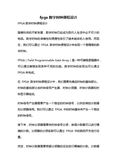
这里以及后面章节提到的时钟域,是指一组逻辑,这组逻辑中的所有同步单元(触发器、同步RAM块以及流水乘法器等)都使用同一个网络作为时钟。
假如设计中所有的触发器都使用一个全局网络,比如FPGA的主时钟输入,那么我们说这个设计只有一个时钟域。
假如设计有两个输入时钟,如图1所示,一个时钟给接口1使用,另一给接口2使用,那么我们说这个设计中有两个时钟域。
图1:双时钟域设计平时我们在设计中遇到的门控时钟、衍生时钟以及事件驱动的触发器都可归为时钟域类别。
如图2所示,通过一个简单门控时钟创建了一个新的时钟域。
我们知道,这类时钟控制在FPGA设计中并不被推崇(可以使用时钟使能替代时钟门控),然而它却非常有利于我们理解时钟域这一概念。
本章我们将着重详细讨论以下主题:•两个不同时钟域之间传输信号。
•亚稳态的产生以及对设计的可靠性的影响•通过相位控制避免亚稳态•在时钟域之间传输单个信号,将信号打两拍•使用FIFO在时钟域之间传输多位数据•使用分区同步器模块提高设计的组织架构•处理ASIC验证原型里的门控时钟•建立一个单时钟模块•自动门控移除图2:通过门控时钟创建的时钟域一、跨时钟域设计中包含多时钟域,首先要解决的是在不同时钟域之间传输信号的问题。
信号跨时钟域传输将会是一个大问题,原因如下:1、信号跨时钟域传输产生的故障总是不太容易复现。
fpga跨时钟域处理方法

fpga跨时钟域处理方法fpga 跨时钟域处理方法1.什么是FPGA跨时钟域处理?FPGA跨时钟域处理是指在FPGA中处理不同的时钟域的信号,把不同的时钟域的信号转换成成某种特定的格式或者特定算法,以便FPGA 能够处理这些不同的时钟域的信号。
2. FPGA跨时钟域处理的优势(1)更低的功耗,由于时钟频率较低,其功耗比信号时钟频率高的系统低得多。
(2)更高的可靠性,由于时钟频率较低,其硬件的可靠性比信号时钟频率更高。
(3)更快的切换和转换速度,在跨时钟域中,由于只需要处理少量的信号,因而切换和转换的速度会更快。
(4)更小的面积,由于少量的信号需要被转换,相应的FPAG占用的面积也会更少。
3. FPGA跨时钟域处理的实现(1)时间轴划分:第一步是将FPGA转换时钟域中需要处理的信号根据频率分类,并将其根据实际应用场景放置在不同的时间轴上,以便进行后续的处理。
(2)位转换和跨域转换:第二步是将这些处理过的信号转换为不同时钟频率域的信号,这种转换可以采用位级或字节级转换等,以便这些信号能够更好的处理。
(3)中转处理:第三步是将不同时钟频率域的信号做一个中转处理,将其转换成FPGA能够处理的信号,再对每个时钟域上的信号进行处理,完成跨时钟域处理。
4. FPGA跨时钟域处理的应用(1)通信领域:一些通信应用中会存在部分接收信号的处理只能在低频率的时钟域上完成,比如协议及协议解析。
采用FPGA跨时钟域处理,可以有效的提高系统的处理能力。
(2)信号处理领域:有不少信号处理应用一般要求高速处理,这就需要高频率的时钟域;而有些信号处理应用却完全不需要,而FPGA跨时钟域处理可以有效解决这个问题,同时又能提高系统的可靠性。
5.总结FPGA跨时钟域处理是将不同时钟域的信号转换为特定类型或特定算法,以便FPGA能够处理这些不同的时钟域的信号。
它具有更低的功耗、更高的可靠性、更快的切换和转换速度以及更小的面积等优势。
FPGA跨时钟域处理的具体步骤包括时间轴划分、位转换和跨域转换、中转处理等。
FPGA时钟设计

FPGA时钟设计在FPGA设计中,时钟设计需要考虑以下几个方面:1.时钟源:时钟源可以是外部信号源,也可以是FPGA内部的时钟发生器。
外部时钟源一般来自外部设备或者振荡器。
FPGA内部的时钟发生器可以根据需要生成所需的时钟频率。
2.时钟分频:时钟分频是指将输入的时钟频率分频为所需的输出频率。
在一些应用中,需要将时钟频率降低到一个更低的频率,以降低功耗或满足特定的应用需求。
3.时钟分配:在FPGA设计中,可能会有多个模块需要使用时钟信号。
时钟分配是指将时钟信号分配给各个模块,以确保它们能够按照同步的方式工作。
4.时钟域划分:在FPGA设计中,可能会存在多个时钟域,即不同的时钟频率和时钟相位。
时钟域划分是指将设计中的电路划分为不同的时钟域,并确保时钟跨域的数据传输正确。
5.时钟驱动和延迟:时钟驱动和延迟是指时钟信号的传输延时。
由于FPGA中的逻辑电路通常具有不同的传输延时,所以时钟信号需要正确地驱动各个子模块,以确保数据的正常传输。
在进行FPGA时钟设计时,需要考虑以下几个关键问题:1.时钟频率选择:时钟频率选择需要综合考虑系统的需求和FPGA的性能。
较高的时钟频率可以提高系统的工作速度,但也会增加功耗和电磁干扰。
较低的时钟频率可以降低功耗和电磁干扰,但会降低系统的工作速度。
2.时钟相位对齐:时钟相位对齐是指在不同时钟域之间进行数据传输时,需要确保时钟相位的对齐。
时钟相位对齐可以通过插入寄存器或者使用FPGA的时钟管理资源来实现。
3.时钟缓冲和驱动:时钟缓冲和驱动是指对时钟信号进行放大和驱动,以确保时钟信号能够正常传输和驱动其他模块。
时钟缓冲和驱动可以使用FPGA内部的时钟管理资源,如PLL和BUFIO等。
4.时钟分频策略:时钟分频策略是指根据需要将时钟频率分频为所需的频率。
时钟分频可以使用FPGA内部的分频器来实现,也可以使用逻辑电路来实现。
在FPGA时钟设计过程中,需要进行时钟约束设置,即设置时钟频率、时钟相位和时钟域等约束条件。
- 1、下载文档前请自行甄别文档内容的完整性,平台不提供额外的编辑、内容补充、找答案等附加服务。
- 2、"仅部分预览"的文档,不可在线预览部分如存在完整性等问题,可反馈申请退款(可完整预览的文档不适用该条件!)。
- 3、如文档侵犯您的权益,请联系客服反馈,我们会尽快为您处理(人工客服工作时间:9:00-18:30)。
没有任何组合逻辑
没有任何组合逻辑
CLOCK1 DOMAIN
DATA
D
CLOCK2 DOMAIN
D
OUTPUT
D
Clock1
MTBF计算一个例子
如何减少亚稳态的风险
▪ 单一时钟域内信号
▪ 工具检查每个触发器的建立保持时间,确保 其不出现亚稳态
▪ 跨时钟域的信号
▪ 没有工具可以保证其可靠性; ▪ 静态时序分析其应该设置false path 约束;
▪ 只能靠逻辑设计来保证:同步化技术。
同步化技术
▪ 根据跨时钟域信号的特点来选择同步化 方法:
D
Clock2
取沿电路-把上升沿转化成脉冲
OUTPUT
D
D
OUTPUT
脉冲同步器-快时钟域到慢时钟域
翻转电路-把脉冲转化成边沿
CLOCK1 DOMAIN
0
Q
1
D
Q\
CLOCK2 DOMAIN
D
Clock1
Clock2
取沿电路-把边沿转化成脉冲
OUTPUT
D
D
OUTPUT
同步器设计推荐的做法
▪ 同步器单独成模块,引入两个独立时钟 ▪ 其他模块都设计为单一时钟模块,完全同要求无法接受的程度。来自如何评估其危害-MTBF
▪ MTBF 定量评估亚稳态对可靠性的影响 ▪ MTBF is a measure of how often, on the average,
a metastable event lasts a time tr or longer. ▪ 下式适用于一级同步寄存
亚稳态
▪ 什么是亚稳态 ▪ 引起亚稳态的原因 ▪ 亚稳态对系统可靠性的危害 ▪ 如何评估其危害-MTBF ▪ 如何减少亚稳态的风险
什么是亚稳态
▪ a metastable output is undefined or oscillates between HIGH and LOW for an indefinite time due to marginal triggering of the circuit. This marginal triggering is usually caused by violating the storage elements’ minimum set-up and hold times.
FPGA跨时钟域设计 -- Multi-Asynchronous Clock Design of FPGA
主要内容
▪ 局部同步设计概念 ▪ 跨时钟域的问题
▪ 亚稳态(metastability) ▪ 同步失败(synchronize failure)
▪ 同步化
▪ 同步器(synchronizer) ▪ 保持寄存器和握手(hold and handshake) ▪ 异步FIFO设计(asynchronous FIFO)
▪ 同步器--控制信号 ▪ 保持寄存器和握手--地址或数据总线信号 ▪ 异步FIFO设计--数据总线信号
同步器(two-stage of flip-flops)
▪ 为什么使用两级寄存器(接收时钟域) ▪ 是一级寄存概率平方,两级并不能完全
消除亚稳态危害,但是提高了可靠性, 减少其发生的概率 ▪ 一级概率很大,三级改善不大 ▪ 同步器延迟-1或2个接收时钟
为什么讨论多时钟域设计
▪ 全同步设计(totally synchronous) ▪ 一个时钟
▪ 全异步设计(totally asynchronous)
▪ 没有时钟
▪ 全局异步,局部同步设计(globally asynchronous,
locally synchronous) 多个独立时钟域,同一时钟域内同步 这是我们关心的多时钟域设计 不可避免,单一时钟不能满足设计的需求
亚稳态最终收敛于0或1或者振荡
引起亚稳态的原因
▪ 在数据跳变期间采样 ▪ 建立或保持时间不满足
▪ 跨时钟域的信号和同步时钟之间的关系不能 确定
▪ 单一时钟域内工具确保建立保持时间,不出 现亚稳态
从tsu ,th和tco的角度看亚稳态
亚稳态对系统可靠性的危害
▪ 同步失败(Synchronize Failure) ▪ 系统失败(System Failure) ▪ 按概率出现;发生概率可能达到可靠性
步模块 ▪ 以时钟域作为信号命名的前缀 ▪ 静态时序分析的时候,对同步器模块异步
输入信号的设定false path:用通配符
使用同步器需要注意的问题
1. 原时钟域的寄存器和新时钟域的两个寄 存器之间都不能有组合逻辑
2. 快时钟域到慢时钟域 3. 多位控制信号跨时钟域 4. 总线信号跨时钟域
同步器寄存器之间的不能有组合逻辑
MTBF
▪ tr-the resolving time allowed for metastable events
▪ tsw-device specific ▪ W-device specific ▪ fc-system clock frequency ▪ fd-average asynchronous data frequency
▪ "When sampling a changing data signal with a clock ... the order of the events determines the outcome.The smaller the time difference between the events, the longer it takes to determine which came first.When two events occur very close together, the decision process can take longer than the time allotted,and a synchronization failure occurs. "
同步器分类
▪ 电平同步器 ▪ 边沿检测同步器 ▪ 脉冲同步器
基本同步器-电平同步器
没有任何组合逻辑
没有任何组合逻辑
CLOCK1 DOMAIN
DATA
D
CLOCK2 DOMAIN
D
OUTPUT
D
Clock1
Clock2
边沿检测同步器-慢时钟域到快时钟域
CLOCK1 DOMAIN
D
Clock1
CLOCK2 DOMAIN