DCMotor_Driver
四极管型号:64QS019E 的三相 brushless DC 电机驱动参考设计文件说明书

Reference Design BriefMotor Drive System Reference series48V power supply, 3 hall sensor support, Three-phase brushless DC motor drive reference design.REFMOT107General DescriptionEvaluation board to drive a 3 Hall sensor three phase brushless DC motor with supply voltage of 48V (typ) and motor current of 8A (max).It consists of a 3 hall sensor three phase brushless DC motor pre-driver and 6 Nch MOSFET s.The rotor position is detected by 3 hall sensors, and the sin wave drive realizes silent and low vibration, and the automatic advance angle control enables highly efficient motor drive.The output MOSFET can be mounted in the TO252 package or the HSOP8 package. In this board, the TO252 package product is mounted.Translated with /Translator (free version) Features⏹ 3 Hall Sensor Three Phase Brushless DC Motor Pre-Driverand Output MOS N+N Configuration⏹Supply voltage 48V(typ)⏹Output current 8A(max)⏹Sine-wave commutation PWM drive, automatic advanceangle control⏹Number of motor poles setting function⏹Soft start function⏹Dead time setting function⏹Power save input/ Rotation direction setting input/ Shortbrake inputApplications⏹Fan motors, other general consumer equipmentWeb pagehttps:///reference-designs/refmot107Key Specifications⏹Name of board:BM64300MUV-EVK-001⏹Input voltage:28V to 63V⏹Nb of outputs:8A(Max)(depending on driving capability of MOSFET)⏹Output voltage: 3 Hall sensor sine-wave commutation drive,automatic advance angle control⏹EMC performance:Input: Control input (PWM), power save, rotation direction setting, short brake.Output: FG output..Board ImageBoard No. W (Typ) x D (Typ)BM64300MUV-EVK-00160mm×68mm Figure 1. BM64300MUV-EVK-001 BoardSystem block diagramFigure 2. shows typical application diagram of REFMOT107 usage.Figure 2. REFMOT107 block diagramBM64300MUV 3 Hall SensorsThree-Phase Brushless Motor Pre-Driver ICVCC50VBAT(48V)3222HUP/HUN HVP/HVN HWP/HWN222HUP/HUN HVP/HVN HWP/HWN VCC50HVVCC50Electrical CharacteristicTable 1 Electrical Characteristics of REFMOT107 Parameter Min Typ Max Unit ConditionsPower supply voltage (VCC)284863Vinternal regulator output4.55.0 5.5V(V CC50)Control input voltage0-V CC50*1VGate Drive Voltage (VG)-VCC+9.5-VOutput current--8APWM Frequency-40-kHzKey components in the designTable 2 Key parts list of REFMOT107Key components Product typeBM64300MUV 3 Hall Sensors Three-Phase Brushless Motor Pre-DriverRD3P175SN Nch 100V 17.5A Power MOSFETLTR18EZPF High Power Chip ResistorDesign support contentsIn the ROHM official web site, various design support contents are available to download. https:///reference-designs/refmot107It is possible to start your pcb design based on design resources such as●Schematic●PCB layout (gerber data)●Parts listNoticeThank you for your accessing to ROHM product informations.More detail product informations and catalogs are available, please contact us.ROHM Customer Support System/contact/。
直流无刷电机(BrushlessDCmotor)

直流无刷电机(Brushless DC motor)0 IntroductionIn the development of the smart car, an important part is that the smart car can adjust the speed and direction of the vehicle independently according to the surrounding obstacles. DC motor speed control system designed in this paper is an important part of the intelligent car, DC motor speed control system is mainly composed of S3C44B0X processor and motor drive chip L298N, the main function is the two wheel drive car, adjust the vehicle speed, by changing the two wheel speed adjustment direction.1 Hardware DesignDesigned by ARM, the ARM processor with RISC architecture has strong performance, low power consumption, small size, and supports Thumb (16 bit) /ARM (32 bit) double instruction set, and the instruction execution speed is fast. At present, ARM series microprocessor has occupied more than 75% market share in the 32 bit RISC embedded products. Especially ARM7TDMI series is the most widely used, and its cost performance is also the highest.1.1 brief introduction of S3C44B0XS3C44B0X is a 16/32 bit RISC processor based on the ARM7TDMI kernel introduced by Samsung. This processor provides a wide range of on-chip peripherals that greatly reduce configuration of components other than the processor in system circuitry. The S3C44B0X has 6 16 bit timers, each of which can operate in either an interrupt mode or a DMA mode. Timers 0, 1, 2, 3, 4 have thePWM function, and timer 5 is an internal timer. Timer 0 and 1, 2 and 3, 4 and 5 respectively, sharing a 8 bit prescaler (Prescaler), the scope of the prescaler value is 0 - 255, three prescaler value through the TCFG0 register set; the timer 0, 1, 2, 3 each have a 5 different frequency signals (1/2, 1/4, 1/8, 1/16, 1/32) clock divider (Divider), timer 4 and 5 are respectively provided with a 4 frequency signal (1/2, 1/4, 1/8, 1/16) clock divider. The segmentation values of the 6 timers are set by register TCFG1.Timer input clock frequency = MCLK/Prescaler/Divider. Among them, MCLK = 60MHz is the dominant frequency of the system.1.2 hardware implementationIn order to improve the system efficiency and reduce power consumption, the power amplifier circuit is based on the bipolar H bridge pulse width modulation (PWM) integrated circuit L298N. L298N SGS is the product of the company, including high voltage and high current driver two H bridge, receiving standard TTL logic level signal to drive a 46 volt, 2 amp motor below the working temperature range from - 25 degrees to 130 degrees. A schematic diagram of a H bridge within it is shown in figure 1. The EnA is a control enable terminal that controls the stop of the motor between the OUTl and the OUT2, and the IN1 and IN2 pins are connected to the control level to control the steering of the motor between the OUTl and the OUT2. When the enable terminal EnA is valid, the IN1 is low, the IN2 is high, the transistor 2, the 3 are connected, and the 1 and 4 are cut off, the motor reverses. When the IN1 and IN2 levels are the same, the motor stops.Another H bridge works the same as above. The motor stop between OUT3 and OUT4 is controlled by EnB, and the steering of the motor between OUT3 and OUT4 is controlled according to the input level of IN3 and IN4 pins.Since the S3C44B0X itself contains 5 PWM outputs, the direct output control signal can be applied to the L298N without additional circuitry. The schematic diagram of the system is shown in figure 2. In the system, timers 1 and 2, which work in interrupt mode, are selected as timers for generating PWM. Through programming, set the I / O port, PE4 and PE5 as the timer 1, 2 output PWM port, access to the L298N EnA and EnB port, according to the timer 1, 2 output PWM frequency control two DC motor speed. PE6 is set to output port, connected to IN1 and connected to IN2 via a reverser; similarly, PE7 is also set to output port, access to IN3, and access to IN4 via a reverse device. By accessing the reverser, the IN1 and the IN2, IN3 and IN4 will not be at the same high or low level, i.e., the motor will not stop because the IN1 and IN2, the IN3 and the IN4 levels are the same.The stop operation of the motor can be achieved by modulating the pulse width to 0, i.e., the duty cycle is 0, or the bit of the timer is turned off. Thus, only one signal PE6 can control the state of IN1 and IN2, and PE7 controls the state of IN3 and IN4, thus reducing the control signals of the system and simplifying the system to a certain extent. In order to ensure the normal work of the L298N driver chip, but also to join in with the DC motor of four diode with current in the motor back EMF generated by the shunt to ground or power, in order to avoidreverse electromotive force damage to L298N.2 software design of the system2.1 timer operation modeIn S3C44B0X, each timer has an inverted timer that drives the 16 bit countdown register TCNTn via the timer clock source. Before the timer starts, write an initial value to the timer count buffer register (TCNTBn), which is loaded into the countdown timer TCNTn when the timer is started. In the timer comparison buffer register (TCMPBn), an initial value is also written. The runtime is used to load into the comparison register TCMPn and compare with the value of the countdown timer TCNTn. When you start the system, you need to load the values of the two buffers, TCMPBn and TCNTBn, into TCMPn and TCNTn by setting the manual refresh bit. The application of these two buffers, i.e., double buffers, of TCMPBn and TCNTBn, allows the timer to produce a stable output at the same time as frequency and duty cycle. The general steps to start the timer are as follows:1) writes the initial value to TCNTBn and TCMPBn.2) set the automatic reload bit of the corresponding timer3) set the manual update bit for the corresponding timer, and the counter is set to the off state4) setting the start bit of the corresponding timer to start the timer and clearing the manual update bit at the same time.At this point, the timer TCNTn starts counting backwards. When the TCNTn has the same value as the TCMPn, the logic level of the TOUTn is changed from low to high. When the counter TCNTn reaches 0, a timer interrupt request is generated, informing the CPU that the timer operation has been completed. At this point, if the auto reload control bit enable, the value of the TCNTBn is automatically loaded into the TCNTn register and the next operation cycle is started. If the timer is stopped by clearing the timer, enabling bits, etc., the count value will not be automatically overloaded.2.2 modulation PWMPulse width modulation (Pulse Width Modulation PWM) means that the basic cycle of the output signal is fixed, and the output power is controlled by adjusting the size of the working cycle in the basic cycle. For a timer, when the frequency of the input clock source is generally unchanged, namely TCFG0 (timer prescaler value) and TCFG1 (timer segmentation value) value after setting no change. This provides a stable clock source for PWM. The speed of the motor is proportional to the voltage at both ends of the motor, and the voltage at both ends of the motor is proportional to the duty cycle of the control waveform. Therefore, the speed of the motor is proportional to the duty cycle, and the larger the duty ratio, the faster the motor is turned. In the system, the PWM pulse frequency is decided by TCNTBn, and the PWM pulse width value is decided by the value of TCMPBn, and the duty cycle is TCMPn/TCNTn. If you want to make the motor speed down, a relatively low output value of PWM pulse width is obtained, can reduce the value of TCMPBn; to makethe motor speed increase, the output of a higher PWM value, can increase the value of TCMPBn. Because of the characteristics of the double buffer, a PWM cycle TCMPBn value by ISR (interrupt service routine) or other means in the current cycle of low level PWM at any point that is written, can be blocked by re setting the value of TCMPBn to change the motor speed in the program. The value of the buffer TCMPBn and TCNTBn is not necessarily equal to the value of the TCMPn, TCNTn of this cycle, but must be the value of the next cycle of TCMPn and TCNTn.2.3 program codeThe application in this article is in ADS1.2 development environment, cross compiled, downloaded to Flash running. Program code (take timer 1 as an example):/ / initialize portVoid, Init_PortE (){RPCONE=0x5a00; / / define I/O port //PE4, PE5, PE6, PE7 / / functionRPUPE=0xf8; / / no resistance of the corresponding bit to pull}Start / / No. A motor, the motor control by timer 1Void, Start_MotorA (){RTCNTB1=Motor_CONT; / / two / / buffer assignment RTCMPB1=Motor_cont;RTCON |= (0x01<<11); / / Auto reload timer 1 RTCON |= (0x01<<9); / / manual refresh set RTCON &= ~ (0x01<<10); / / close reverserRTCON |= (0x01<<8); / / start timer 1RTCON &= ~ (0x01<<9); / / clear manual refresh bit }//A motor stopVoid, Stop_Motor1 (){RTCON &= ~ (0x01<<8); / / clear enable bit timer 1 }/ / change the duty ratio and the steering motorVoid SetPWM (int, valueA, int, drct){RPDATE=drct; / / drct definition PE6 output high level or low level, to control motorRTCMPB1=Motor_COUNT*valueA/0x64; //valueA is the duty cycle can be set to valueA for 0 A to make the motor stop / stop rotation.}Other motor settings are the same as above. The moving speed of the two groups of PWM can be changed at the same time, and the running speed of the car can be adjusted. By setting two different duty cycles, the speed difference between the two wheels is formed, and the purpose of changing the driving direction is achieved.In contrast, 1KHz 100Hz, 10KHz PWM, the output of the driving motor is found when the frequency was 100 Hz, the motor running in clearance rotational state; when the frequency is 10KHz, the motor running instability; when the frequency is 1KHz, the different duty ratio motor operation is very smooth, the speed and the direction of change quickly. Fig. 3 is a modulation waveform produced by an oscilloscope with an PWM frequency of 1KHz, a duty ratio of 30%, and an inversion of the motor.3 conclusionIn this paper, the output frequency of PWM is 1KHZ, and the DC motor is 120 revolutions per minute. The rated voltage is 12V (no additional inductive load outside the motor). The final realization of this subject is the embedded intelligent vehicle system based on ARM, and the PWM speed control of DC motor is one of the important subsystems. The experiment proves that the 16/32 bit RISC processor Samsung of S3C44B0X company is convenient to realize the modulation PWM, programmable, and the motor speed and steering change rapidly without pause, so it can serve the smart car very well.Source: 08, my loveSource of technical data: zhangwrThis article is for learning, reference, use, copyright belongs to the author.Because the content of this website is more and cannot contact the author in time, please contact us according to the method displayed on this website.Design and implementation of DC motor speed regulation system based on ARM0 Introduction in the development of the smart car, an important part is that the smart car can adjust the speed and direction of the vehicle independently according to the surrounding obstacles. The DC motor speed control system designed in thispaper is one of the smart cars...Design of Embedded Ethernet based on S3C44B0X mu cLinuxWith the rapid development of semiconductor technology, embedded products have been widely used in military, consumer electronics, network communications, industrial control and other fields. Networking is an inevitable trend of embedded system development. Embedded Linux acts as an open source...Development of embedded application based on ClinuxThe range of embedded systems is very extensive. From simple SCM systems to non computer systems operating at several hundred megabytes, operating systems can be referred to as embedded systems. With the increasing demand for electronic systems in all industries,Embedded systems are also becoming more and more...Application of Microwindows based on S3C44B0X in remote infrared meter reading systemWith the extensive application of embedded systems, the demand for embedded products for human-computer interaction is becoming larger and larger, and the design of GUI is becoming more and more important. Vendors who develop real-time embedded systems over Linux will typically choose the following GUI systems...About Samsung S3C44B0X target board uClinux BootloaderUClinux is an embedded Linux operating system designed for the control domain. It follows most of the main features of the mainstream Linux and has been reduced to a certain extent. The design is primarily aimed at microprocessors without memory management units (MMU), such as ARM7...。
BDR6133扫地机专用马达驱动芯片
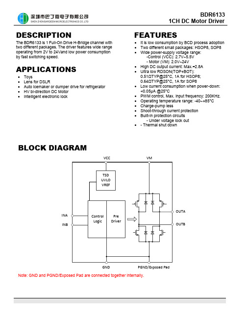
DESCRIPTIONAPPLICATIONS∙ Toys∙ Lens for DSLR∙ Auto icemaker or dumper drive for refrigerator ∙ HV bi-direction DC Motor ∙Intelligent electronic lock- Motor (VM): 2.0V~24V∙ High DC output current: Max.=2.8A ∙ Ultra low RDSON(TOP+BOT): 0.51ΩTYP@25°C , 1A for HSOP8; 0.64ΩTYP@25°C , 1A for SOP8∙ Low current consumption when power-down: <0.05μA @25°C∙ PWM control, Max. input frequency: 200KHz. ∙ Operating temperature range: -40~+85°C ∙ Charge-pump less∙ Shoot-through current protection ∙ Built-in protection circuits- Under voltage lock out ∙ - Thermal shut downBLOCK DIAGRAMINA INBGND PGND/Exposed PadOUTAOUTBNote: GND and PGND/Exposed Pad are connected together internally.APPLICATION CIRCUITSSOP8/HSOP8ORDER INFORMATIONPIN CONFIGURATIONSOP8 HSOP8PIN DESCRIPTIONFUNCTION TABLEINPUT-OUTPUT LOGIC TABLEFUNCTION SEQUENCEVMVCCINAINBOUTAOUTBStandby Reverse Forward Brake Standby Note: VM & VCC power on have no timing sequenceVM & VCC power off have no timing sequencePROTECTION FUNCTIONTHERMAL SHUTDOWN (TSD) CIRCUITThe BDR6133 includes a thermal shutdown circuit, which turns the output transistors off when the junction temperature (Tj) exceeds 175°C (typ.).The output transistors are automatically turned on when Tj cools past the shutdown threshold, which is lowered by a hysteresis of 30°C.TSD = 175°CΔTSD = 30°C* In thermal shutdown mode, the circuits powered by VCC are work normal, and the circuits powered by VM are shut down.UNDER VOLTAGE LOCKOUT (UVLO) CIRCUITThe BDR6133 includes an under voltage lockout circuit, which puts the output transistors in the high-impedance state when VCC decreases to 2.13V (typ.) or lower.The output transistors are automatically turned on when VCC increases past the lockout threshold, which is raised to 2.21 V by a hysteresis of 0.08 V.*In UVLO shutdown mode, a part of circuits powered by VCC are work normal, and the circuits powered by VM are shut down.SHOOT-THROUGH CURRENT PROTECTIONDuring Dead Time (Shoot through current circuit is operated.), Power MOS both of HI side and Low side are turned off. But in this time, internal parasitic diode is turned on according to current direction.ABSOLUTE MAXIMUM RATINGSNotes:1. Terminal OUTA,OUTB pulse with =<200ms:Duty 5%2. Terminal OUTA,OUTB pulse with =<200ms:Duty 1%3. Maximum power dissipation is a function of TJ(max), Rja, and TA. The maximum allowable power dissipation at any allowable ambienttemperature is PD = (TJ(max) − TA)/Rja. Operating at the absolute maximum TJ of 150°C can affect reliability.4. The package thermal impedance for HSOP8 is calculated in accordance with JEDEC, 2S2P test PCB, Rja=41℃/W5. The package thermal impedance for SOP8 is calculated in accordance with JEDEC, 2S2P test PCB,Rja=113.5℃/W RECOMMENDED OPERATION CONDITIONSELECTRICAL CHARACTERISTICSSWITCHING CHARACTERISTICS WAVEFORMSWITCHING WAVEFORMINAINB100%50%50%100%TfONHTfOFFHDRIVER 90%50%10%-90%-50%-10%TffTfr100%50%50%100%TrONHTrOFFH90%50%10%-90%-50%-10%TrrTrf100%-100%-100%100%Electric current in the OUTA —OUTB direction is being made (+)=forward rotationFig.1 switching characteristics waveformINAINB100%50%TfONHTfOFFHDRIVER90%50%10%Tff100%50%TrONH90%50%10%Trr 100%100%Electric current in the OUTA —OUTB direction is being made (+)=forward rotationFig.2 switching characteristics waveformPCBLAYOUT 8-PIN, HSOP8-PIN, SOPPACKAGE INFORMATION 8-PIN, HSOPNotes:1. Refer to JEDEC MS-012 BA2. All dimensions are in millimeter.8 PINS, SOPNotes:1. Refer to JEDEC MS-012 AA2. All dimensions are in millimeter.。
电气自动化专业的英语简历(5篇模版)

电气自动化专业的英语简历(5篇模版)第一篇:电气自动化专业的英语简历电气自动化专业的英语简历范文时光在流逝,从不停歇,许多朋友又将开始寻求新的工作机会,是时候好好地琢磨一下写简历的事情了哦。
你真的.懂得怎么写好简历吗?以下是小编为大家收集的电气自动化专业的英语简历范文,仅供参考,大家一起来看看吧。
Name: Nguyen xxsex: MaleDate of birth: 1986-6National: HanPlace of residence are: Liaoning Province / Dandong CityMarital status: unmarriedEducation: tertiaryGraduate school: University of Shashi in Hubei ProvinceProfession: Electrical AutomationSelf-evaluationIn the young season, I willing to endure hardship involved, only through their own enthusiasm, pro-active efforts to achieve their own values and work to make the GREatest contribution: As a beginner, I have an excellent ability to learn and willing to learn, innovate, constant pursuit of excellence;as a participant, I have an honest and credible character, full of team spirit;as a leader, I am able to work with, and decisive style, good communication and interpersonal coordination.Have a strong endurance, willpower and the quality of tradition of hard work, serious and responsible work, positive and agGREssive personality persistent optimism, the courage to face the difficulties and challenges Educational background20xx.9 ~ 20xx.6 University, majoring in professional Shashi: Electrical Automation Education: tertiaryMajors:College English, advanced mathematics, engineering, mathematics, University physics, mechanical drawing, circuit and magnetic circuit, Analog Electronics, Digital Electronics, Automatic Control Theory, Principle and Application of Microcomputer, ALGOL, electrical and drag the basis of the semiconductor variable technology, engineering, testing, factory electrical equipment, automation systems, power plants, Introduction to Business Management.In school honors: 20xx and 20xx, respectively, in 20xx the school won the men's basketball championship in school students were hired as the sportsdepartment, Deputy Minister ofIn June 20xx the school of electrical technology to obtain professional credentialsIn June 20xx in the school to obtain vocational qualification certificate ElectricianLanguage Proficiency: Mandarin: fluent English: 2Professional skills:1.I am the 20xx graduates, after three years of training in schools, the community has a certain deGREe of adaptability, professionalism and strong sense of responsibility, diligence, meticulous and comprehensive analysis of strong ability and learning ability.At school, I attended the school of professional training, such as: 7-assembled radios, electronic form design simple curriculum design, electrician, electrical technology applications, such as training, and obtain the relevant certificate.In the classroom, I have also systematically studied the principle of automatic control, process control instrumentationand automation, sensor technology infrastructure, micro-computer control technology, MCS-51 single-chip application of the principle and examples of the basis of motor and electric drive, power electronics Technology, Microcomputer Principle and Interface Technology, programmable controller programming methods and engineering applications(PLC), the number of sub-electronic technology, analog electronic technology, CAD drawings, etc., have a certain amount of professional knowledge;2.Familiar with the 51 series single-chip and application of the principle.Understanding of the structure of 51 single-chip and software programming(Wei Fu E6000 / compile /), 51 single-chip based on the understanding of the DC motor driver, LED display, keyboard control and sensors, such as software and hardware design.3.Can be of conventional electrical equipment installation, debugging and fault diagnosis and treatment;4.With maintenance, debugging and automatic control system for automatic detection systems;5.Familiar with using the WINDOWS operating system, OFFICE office software.Job search intention:Work type: Full-timeI hope the industry: home appliances for sale | Electrical | Electronics / Semiconductor / Instrument Instrument Salary expectations: Discuss why the provision of housing 第二篇:电气自动化简历个人概况姓名:详详细细性别:男籍贯:山西省长治市民族:汉贴照片出生日期:1990.11.02政治面貌:团员联系电话:电子邮箱:通讯地址:江苏省南京市玄武区孝陵卫200号求职意向电子或电气工程师;电气设备维修,工仪表开发与销售;小型PLC编程;电工电子类工作;供配电应用;教育背景◆ 2009/9–2013/7南京理工大学电气工程及其自动化本科主干课程电路、数字电路、模拟电路,信号与系统、微型计算机原理及应用、电力系统分析、电力系统与继电保护、PLC原理及应用、c++、单片机原理及应用、DSP、控制工程基础、电力电子技术、工程电磁场、电机学等个人证书◆2009/12:全国英语四级证书◆2010/3:校二等奖学金◆2011/03:江苏计算机二级证书◆2011/3:校三等奖学金◆2011/9:江苏计算机三级证书◆2011/12:全国英语六级证书社会实践◆ 2011.7到2011.8在苏宁公司参加了实习,主要负责空调等电器的安装和维护◆ 2010.9到2011.12在学校进行电工实习,学会了一般的电子实践操作,例如绘制PCB电路、制作PCB电路板、焊接、调试等,最终做出一个声控灯和一个调频收音机;◆ 2011.3到2011.6进行金工实习,亲手操作包括数控机床在内的各种机床,初步学会了车、铣、磨、钻、焊等加工方法,通过学习初步学会了数控车床的使用。
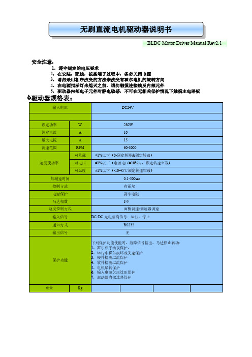
无刷电机驱动器说明书
80
58
120
重量
Kg
驱动器接品图
无刷直流电机驱动器说明书
BLDC Motor Driver Manual Rev2.1
BLDC MoTor river
浅绿色 粉红色
棕色 白色
橙色(+5V) 紫色(SP) 灰色(GND)
绿色(复位) 红色(+5V) 黑色(GND) 蓝色(RXD) 黄色(TXD)
开/停 启停控制线 无水断电开关
控制方式
有霍尔电源保护刹车电阻马达相数 速度控制方式
输入信号
3Φ 面板调速/调速器调速 DC-DC 光电隔离信号:运行,停止
通讯方式 输出信号
RS232 无
保护功能
下列保护功能使能时,故障信号输出,马达停止转动:
1,霍尔相序错误保护, 2,运行中霍尔损坏或失速保护 3,硬件检测过流保护 4,软件检测过流保护 5,电机堵转保护 6,输入电源欠压过压保护 7,驱动器内部过热保护
驱动器规格表:
输入电压
DC24V
额定功率
W
额定电流
A
最大电流
A
调速范围
RPM
对负载
速度变动率
对电压
对温度
加减速时间
280W 10 15 60-3000 ±1%以下(0-额定转矩&额定转速) ±1%以下(电源电压±10%内,额定转速空载) ±1%以下(-10-45℃额定转速空载) 0.1-500sec
无刷直流电机驱动器说明书
BLDC Motor Driver Manual Rev2.1
安全注意:
1,遵守规定的电压要求 2,在安装,配线,拔插端子过程中,务必关闭电源 3,请勿采用相序改变的方法来改变有霍尔电机的旋转方向 4,在电源指示灯未熄灭之前,请勿触摸连接线及内部元件 5,驱动器内部电子元件对静电敏感,不可在无相关保护情况下触摸主电路板
直流无刷电机PWM驱动芯片设计

为了整体的安全性和功能完善性。加入了超前角的调节,死区时间和一些保护电路。 本文定量分析了各模块的实现原理和电路形式,采用10V 0.35I.tmBCD工艺实现电 路,并使用Cadence Spectre工具完成的电路功能的仿真和验证。
关键词:电机驱动芯片;直流无刷电动机;开关损耗最小PWM;正弦波调制
调制波的波形由三要素确定,幅度,相位和频率。本文先理论分析了调制波的函数 表达式,接着研究了三要素量在电路上的信号体现方式,最后结合三要素的信号表达 采用电阻网络拟合出调制波。调制波在与芯片内部生成的三角载波进行比较,比较后 的脉冲波作用到三相全桥逆变器电路,从而实现了对电机转速,转向的控制。
另外,这种调制方法在电机起动,改变转向时不起作用,所以又采用了方波PWM 调制作为补偿调制方式,方波PWM采用两两通电方式。
方面伺服电动机占优,但在电机效率,速度,稳定性,最高转速方面两者相差不大。
最主要的是无刷电动机价格优势很大,要便宜1/3。 表1-1无刷直流电动机与异步电动机主要特性比较【2】
无刷直流电动机
异步电动机
转速范围Jr/mini 转速比
80.4000 1:50
200.2400 1:20
最大输入电流(惯性负载)
西南交通大学 硕士学位论文 直流无刷电机PWM驱动芯片设计 姓名:曾泫鸿 申请学位级别:硕士 专业:计算机系统结构 指导教师:靳桅
201205
西南交通大学硕士研究生学位论文
第1页
Hale Waihona Puke 摘要随着节能减排的严峻,无刷直流电动机以其高的电机效率,宽调速比,可靠的运 行,得以广泛的应用。现在市面上流行的主要是带霍尔位置传感器的电机。这种传感 器价格低廉但位置定位不是很精准。为了提高这类电机的控制能力,本设计采用了开 关损耗最小PWM调制。相对常见的方波PWM调制,显著降低了绕组电流的谐波分量, 提高了运行的稳定性。另外相对于一般的正弦波调制(SPWM),开关损耗减少了1/3, 线电压输出能力提高了2/x/3倍。
无刷马达与有刷马达之差异DCBLMOTOR的结构原理马达

1、應用於冷凍空調的 DCBL MOTOR -1
壁掛型送風馬達:
電氣規格範圍: •Vbus:DC 35V、300~350V •轉速範圍:300~1300RPM (V-com:1.8~6.5V) •額定輸出:10~40W↓ •F.G 信號輸出 •驅動器內置馬達
1、應用於冷凍空調的DCBL MOTOR –2~1
台北喜來登大飯店
標準房(1111 號房)—空調噪音&耗電測試比較表
送風機 HIGH
空調噪音比較表
AC 三速送風機
DC VAV 變頻送風機
50 dB
43 dB
減低噪音值 (dB) 7 dB ↓ 14%
MID
48 dB
39 dB
9 dB ↓ 19%
LOW
2-1、產品可依 (1)水壓 (2)水流量感測控制成為 恆壓泵 / 定流量泵 。
2-2、船用泵設計 DC24V/DC48V (應用船上電源)。 2-3、家用泵設計 AC110V/220V 50/60Hz In 之恆壓泵
(節能/安靜)。 2-4、工業用設計AC單相/三相 220V/380V In 之
恆壓泵(油/水)或定流量泵(節能/減碳) 。 2-5、農業用噴霧機。 2-6、加濕機 / 造霧機。
*可輸出轉速回授,依風量、風壓、溫度 控制要求,適時提共外部控制使用,調 整馬達轉速達到工作要求。
*經由AC電源直接起動馬達,瞬間起動運 轉噪音大。
* 單相交流感應馬達轉速變化需使用使 用輔助線圈及起動電容,透過繼電器 切換達到轉速變化,且轉速固定無法 適時提供轉速回授,效率低。
晶电A3906低电压步进电机驱动器说明书

DescriptionDesigned for pulse width modulated (PWM) control of low voltage stepper motors, and single and dual DC motors, the A3906 is capable of output currents up to 1 A per channel and operating voltages from 2.5 to 9 V .The A3906 has an internal fixed off-time PWM timer that sets a peak current based on the selection of a current sense resistor. An overcurrent output flag is provided that notifies the user when the current in the motor winding reaches the peak current determined by the sense resistor. The fault output does not affect driver operation.The A 3906 is provided in a 20-contact, 4 mm × 4 mm, 0.75 mm nominal overall height QFN, with exposed pad for enhanced thermal dissipation. It is lead (Pb) free, with 100% matte tin leadframe plating.Applications include the following:▪ Digital still cameras (DSC)▪ Cell phone cameras ▪ USB powered devices ▪ Battery powered devicesFeatures and Benefits▪ 2.5 to 9 V operation▪ Internal PWM current limit control▪ Synchronous rectification for reduced power dissipation ▪ Peak current output flag ▪ Undervoltage lockout ▪ Low R DS(on) outputs ▪ Small package▪ Brake mode for DC motors ▪ Sleep function▪ Crossover-current protection ▪ Thermal shutdownLow V oltage Stepper and Single/Dual DC Motor DriverPackage: 20-contact QFN (suffix ES)Typical ApplicationsA3906Approximate sizeDual DC motor applicationStepper motor applicationAbsolute Maximum RatingsCharacteristicSymbol NotesRating Units Load Supply Voltage V BB 9.6V Logic Input Voltage Range V IN –0.3 to 7V Sense Voltage V SENSEx Continuous 0.5V Pulsed, t w < 1 μs1V Output CurrentI OUT May be limited by duty cycle, ambient temperature, and heat sinking. Under any set of conditions, do not exceed the specified current rating or a junction temperature of 150°C.Continuous 1A Peak, DC < 30% 1.5A Output Current in Paralleled OperationI OUT(par)Continuous 2A Peak, DC < 30%2.5A Operating Temperature Range T A Range S–20 to 85°C Junction Temperature T J(max)150°C Storage Temperature RangeT stg–40 to 150°CSelection GuidePart NumberPackingPackageA3906SESTR-T1500 pieces per 7-in. reel20-pin QFN with exposed thermal padThermal Characteristics may require derating at maximum conditions, see application informationCharacteristicSymbolTest Conditions*Value UnitsPackage Thermal ResistanceR θJA4-layer PCB based on JEDEC standard37ºC/W*Additional thermal information available on the Allegro website.Terminal List TableNumberName Function1CP2Charge pump capacitor terminal 22GND Ground3SLEEP Sleep logic input, active low 4IN1Control input 5IN2Control input6IN3Control input 7IN4Control input8FL1Current limit flag, bridge 19FL2Current limit flag bridge 210OUT2A DMOS full-bridge 2, output A11SENSE2Current sense resistor terminal, bridge 212OUT2B DMOS full-bridge 2, output B 13VBB Supply Voltage14OUT1B DMOS full-bridge 1, output B15SENSE1Current sense resistor terminal, bridge 116OUT1A DMOS full-bridge 1, output A 17VCP Reservoir capacitor terminal18CP3Charge pump capacitor terminal 319CP1Charge pump capacitor terminal 120CP4Charge pump capacitor terminal 4–PADExposed pad for enhanced thermal performancePAD1514131211123456789102019181716C P 4C P 1C P 3V C PO U T 1AI N 3I N 4F L 1F L 2O U T 2A SENSE1OUT1B VBB OUT2B SENSE2CP2GND SLEEPIN1IN2Pin-out DiagramFunctional Block DiagramELECTRICAL CHARACTERISTICS1,2 valid at T A = 25°C and V BB = 2.5 to 9 V, unless otherwise notedCharacteristics Symbol TestConditions Min.Typ.Max.UnitsOperating Voltage Range V BB 2.5–9VVBB Supply Current I BB I OUT = 0 mA, PWM = 50 kHz, Duty Cycle = 50% – 5 – mA I OUT = 0 mA, outputs disabled, V BB = 9.6 V– 3 – mA Sleep mode, V IN < 0.4 V– 150500nAOutput Resistance R DS(on)Source driver, I OUT = 400 mA , V BB = 3 V, T J = 25°C – 0.52 0.60ΩSource driver, I OUT = 400 mA , V BB = 3 V, T J = 85°C– 0.78– ΩSink driver, I OUT = 400 mA, V BB = 3 V, T J= 25°C – 0.62 0.74ΩSink driver, I OUT = 400 mA, V BB = 3 V, T J= 85°C – 0.93 – ΩCurrent Trip Sense Voltage V SENSE FLx falling edge160200240mV Clamp Diode Voltage V f I = 400 mA – – 1V Output Leakage Current I DSS Outputs,V OUT = 9 V –20 –20μA Control LogicLogic Input Voltage V IN(1) 2.0–5.5V V IN(0) ––0.8VLogic Input Current I IN(1)V IN = 5.5 V – <100 500nA I IN(0)V IN = 0.8 V – <–100 –500 nAInput Hysteresis V INhys –150–mV¯S¯¯L¯¯E¯¯E¯¯P¯ Input V SLEEP(0) ––0.4V V SLEEP(1) 2 – – VFault Output V FLx Flag asserted, I FLx = 1 mA – – 200mVFault Output Leakage Current I FLx V FLx = 5 V – – 1μAFault Output Timer t FLx Reset of PWM latch – 300 – μsBlank Time t BLANK 2.133.9μsFixed Off-Time t OFF –30–μsPropagation Delay Time t pd(on)Input high to source on, input low to source off 100235350ns t pd(off)Input low to sink off, input high to sink on 50100200nsProtection CircuitryCrossover Delay t COD 200425650ns VBB Undervoltage Lockout Threshold V BBUVLO V BB rising 2.2 2.31 2.45VVBB Undervoltage Lockout Hysteresis V BBUVHYS200 300 400mVThermal Shutdown Temperature T JTSD– 165 – °CThermal Shutdown Hysteresis T JTSDHYS –15–°C 1For input and output current specifications, negative current is defined as coming out of (sourcing) the specified device pin.2Specifications over the operating temperature range are assured by design and characterization.FLxNOTE:Timer resets after each reset of the PWM latch.Control LogicDC Motor OperationIN1 IN2 IN3 IN4 OUT1A OUT1B OUT2A OUT2B Function0 0 0 0 Off Off Off Off DisabledHighLow Forward1 0 1 0 HighLowHigh ReverseLow0 1 0 1 LowHighLow Brake1 1 1 1 LowLowLowStepper Motor OperationOUT2AOUT2B Function IN1 IN2 IN3 IN4 OUT1AOUT1B0 0 0 0 Off Off Off Off Disabled Disabled1 0 1 0 High Low High Low Full Step 1 ½ Step 1Step2Low –½High0 0 1 0 Off Off0 1 1 0 Low High High Low Full Step 2 ½ Step 34StepOff Off –½High0 1 0 0 Low0 1 0 1 Low High Low High Full Step 3 ½ Step 5Step6High –½0 0 0 1 Off Off Low1 0 0 1 High Low Low High Full Step 4 ½ Step 78Low Off Off –½1 0 0 0 HighStepDevice Operation The A3906 is a dual full-bridge low volt-age motor driver capable of operating one stepper motor, two DC motors, or one high current DC motor. MOSFET output stages substantially reduce the voltage drop and the power dissipation of the outputs of the A3906, compared to typical drivers with bipolar transistors.Output current can be regulated by pulse width modulating (PWM) the inputs. In addition supporting external PWM of the driver, the A3906 limits the peak current by internally PWMing the source driver when the current in the winding exceeds the peak current, which is determined by a sense resistor. A fault output notifies the user that peak current was reached. If internal current limiting is not needed, the sense pin should be shorted to ground.Internal circuit protection includes thermal shutdown with hyster-esis, undervoltage lockout, internal clamp diodes, and crossover current protection.The A3906 is designed for portable applications, providing a power-off low current sleep mode and an operating voltage of 2.5 to 9 V.External PWM Output current regulation can be achieved by pulse width modulating the inputs. Slow decay mode is selected by holding one input high while PWMing the other input. Hold-ing one input low and PWMing the other input results in fast decay. Refer to the Applications Information section for further information.Blanking This function blanks the output of the current sense comparator when the outputs are switched. The comparator output is blanked to prevent false overcurrent detections due to reverse recovery currents of the clamp diodes or to switching transients related to the capacitance of the load. The blank time, t BLANK, is approximately 3 μs.Sleep Mode An active-low control input used to minimize power consumption when the A3906 is not in use. This dis-ables much of the internal circuitry including the output drivers, internal regulator, and charge pump. A logic high allows normal operation. When coming out of sleep mode, wait 1.5 ms before issuing a command, to allow the internal regulator and charge pump to stabilize.Enable When all logic inputs are pulled to logic low, the outputs of the bridges are disabled. The charge pump and internal cir-cuitry continue to run when the outputs are disabled.Charge Pump (CP1, CP2, CP3, and CP4) When supply volt-ages are lower than 3.5 V, the two-stage charge pump triples the input voltage to a maximum of 7 V above the supply. The charge pump is used to create a supply voltage greater than V BB, to drive the source-side DMOS gates. For pumping purposes, a 0.1 μF ceramic capacitor should be connected between CP1 and CP2, and between CP3 and CP4. A 0.1 uF ceramic capacitor is required between VCP and VBB, to act as a reservoir to operate the high-side DMOS devices.Thermal Shutdown The A3906 will disable the outputs if the junction temperature reaches 165°C. When the junction tempera-ture drops 15°C, the outputs will be enabled.Brake Mode When driving DC motors, the A3906 goes into brake mode (turns on both sink drivers) when both of its inputs are high (IN1 and IN2, or IN3 and IN4). There is no protection during braking, so care must be taken to ensure that the peak current during braking does not exceed the absolute maximum current.Internal PWM Current Control Each full-bridge is controlled by a fixed off-time PWM current control circuit that limits the load current to a desired value, I TRIP. Initially, a diagonal pairof source and sink DMOS outputs are enabled and current flows through the motor winding and the current sense resistor, RSx. When the voltage across RSx equals the internal reference volt-age, the current sense comparator resets the PWM latch, which turns off the source driver.The maximum value of current limiting, I TRIP(max) , is set by the selection of the sense resistor, RSx, and is approximated by a transconductance function:I TRIP(max) = 0.2 / R S .It is critical to ensure the maximum rating on SENSEx pins (0.5 V) is not exceeded.Synchronous Rectification When a PWM off-cycle is trig-gered by an internal fixed off-time cycle, load current recirculates in slow decay SR mode. During slow decay, current recirculates through the sink-side FET and the sink-side body diode. The SR feature enables the sink-side FET, effectively shorting out the body diode. The sink driver is not enabled until the source driver is turned off and the crossover delay has expired. This feature helps lower the voltage drop during current recirculation, lower-ing power dissipation in the bridge.Overcurrent Output Flag When the peak current (set by the external resistor) is reached, the fault pin, FLx, is pulled low. When a reset of the PWM latch occurs, the fault timer begins. At each PWM latch reset, the timer is reset to zero. After approxi-mately 300 μs, if no peak current event was triggered, the timer expires and the fault is released. This ensures that during PWM current limiting, the fault pin remains in a fault state.Functional DescriptionApplications InformationVV V V IN1IN2IN3IN4+V BB R –V BB R I OUT1 ,I OUT2I OUT3 ,I OUT4+V BB R –V BB RGND GND+I REG0 A-I REGIN1,IN3IN2,IN4I OUTxV IN(1)V IN(1)External PWM If external PWM is used, the internal current control can either be disabled by shorting the SENSEx pin toground, or it can be used to limit the peak current to a value under the stall current to prevent motor heating. External PWM IN1 control is shown in the upper figure.Stepper Motor Control The A3906 also can be used to control a bipolar stepper motor. The control logic for stepper motor control is shown in the lower figure. The driver is capable of operating in full- and half-step modes.PWM current control in fast and slow decay modesStepper motor control in full- and half-step modesParallel Operation The A3906 can be paralleled for applica-tions that require higher output currents. In paralleled mode the driver can source 2 A continuous. The A3906 has two completely independent bridges with separate overcurrent latches. This allows the device to supply two separate loads, and as a result, when paralleled it is imperative that the internal current control is disabled by shorting the sense pins to ground.Because the overcurrent trip threshold is internally fixed at 0.2 V, the trace resistance must be kept small so the internal current latch is not triggered prematurely. With acceptable margin, the voltage drop across the trace resistance should be under 0.1 V. Ata peak current of 2.5 A, the trace resistance should be kept below40 mΩ to prevent false tripping of the overcurrent latch.Each bridge has some variation in propagation delay. During this time it is possible that one bridge will have to support the full load current for a very short period of time. Propagation delays are characterized and guard banded to protect the driver from damage during these events.Layout The printed circuit board should use a heavy ground-plane. For optimum electrical and thermal performance, theA3906 must be soldered directly onto the board. On the under-side of the A3906 package is an exposed pad, which provides a path for enhanced thermal dissipation. The thermal pad should be soldered directly to an exposed surface on the PCB. Thermal vias are used to transfer heat to other layers of the PCB.Grounding In order to minimize the effects of ground bounce and offset issues, it is important to have a low impedance single-point ground, known as a star ground, located very close to the device. By making the connection between the exposed thermal pad and the ground plane directly under the A3906, that areaDC Motor Operation (Parallel Bridge)IN1/IN3IN2/IN4OUT1A/2A OUT1B/2B Function 00OFF OFF Disabled 10H L FOR01L H REV11L L BRAKEPCB Layoutbecomes an ideal location for a star ground point. A low imped-ance ground will prevent ground bounce during high current operation and ensure that the supply voltage remains stable at the input terminal. The recommended PCB layout shown in the diagram below, illustrates how to create a star ground under the device, to serve both as low impedance ground point and thermal path.The two input capacitors should be placed in parallel, and as close to the device supply pins as possible. The ceramic capaci-tor should be closer to the pins than the bulk capacitor. This is necessary because the ceramic capacitor will be responsible for delivering the high frequency current components.Sense Pins The sense resistors, RS x , should have a very low impedance path to ground, because they must carry a large cur-rent while supporting very accurate voltage measurements by the current sense comparators. Long ground traces will cause additional voltage drops, adversely affecting the ability of the comparators to accurately measure the current in the windings. As shown in the layout below, the SENSE x pins have very short traces to the RS x resistors and very thick, low impedance traces directly to the star ground underneath the device. If possible, there should be no other components on the sense circuits.Note: When selecting a value for the sense resistors, be sure not to exceed the maximum voltage on the SENSE x pins of ±500 mV .ES Package, 20-Contact QFN with Exposed Thermal PadCopyright ©2008-2013, Allegro MicroSystems, LLCAllegro MicroSystems, LLC reserves the right to make, from time to time, such de p ar t ures from the detail spec i f i c a t ions as may be required to permit improvements in the per f or m ance, reliability, or manufacturability of its products. Before placing an order, the user is cautioned to verify that the information being relied upon is current.Allegro’s products are not to be used in life support devices or systems, if a failure of an Allegro product can reasonably be expected to cause the failure of that life support device or system, or to affect the safety or effectiveness of that device or system.The in f or m a t ion in c lud e d herein is believed to be ac c u r ate and reliable. How e v e r, Allegro MicroSystems, LLC assumes no re s pon s i b il i t y for its use; nor for any in f ringe m ent of patents or other rights of third parties which may result from its use.For the latest version of this document, visit our website:1A Terminal #1 mark areaCoplanarity includes exposed thermal pad and terminalsB Exposed thermal pad (reference only, terminal #1 identifier appearance at supplier discretion)For Reference Only(reference JEDEC MO-220WGGD)Dimensions in millimetersExact case and lead configuration at supplier discretion within limits shown C D CReference land pattern layout (reference IPC7351 QFN50P400X400X80-21BM)All pads a minimum of 0.20 mm from all adjacent pads; adjust as necessary to meet application process requirements and PCB layout tolerances; when mounting on a multilayer PCB, thermal vias at the exposed thermal pad land can improve thermal dissipation (reference EIA/JEDEC Standard JESD51-5)PCB Layout Reference View。