IGBT模块的并联使用技术指南
IGBT的并联使用
IGBT的并联使用并联使用IGBT组成开关器件可以使整个系统得到更高的额定电流,但是设计并联系统时必须考虑一些重要问题,如模块特性、驱动电路以及电路的布局,这些因素影响着并联支路的电流分配,可能导致并联的每个IGBT电流分配不均衡。
其中,模块特性中的伏安特性主要影响静态运行时的电流分配,转移特性和驱动电路以及布局主要影响动态运行时的电流分配。
由于电流分配的不均衡,使n个IGBT并联的额定电流并不等于n倍的单个模块的额定电流,所以对并联IGBT 模块必须降额使用。
在设计IGBT并联系统时,首先要确定合适的并联模块数目以获得足够的额定电流,同时要保证每个模块工作时不超出安全工作区。
另外需要注意的是,并联使用IGBT模块有助于减小通态损耗,但是开关损耗不会减小,甚至可能增大,尤其在开关频率比较高的时候。
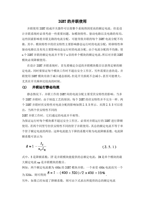
(1)并联运行静态均流静态情况下,并联工作的IGBT间的电流分配主要受伏安特性的影响。
当多个IGBT并联时,由于制造工艺的原因,每个IGBT的伏安特性并不完全一样。
两个IGBT并联时伏安特性对电流分配的影响如图2.5.5所示。
从图2.5.5可以看出,当两个伏安特性不同的IGBT并联工作时,它们通过的电流并不相等。
为保证运行时每个模块都不超过安全工作区,必须对并联运行的IGBT进行降额使用。
若两个同型号但伏安特性不同的管子并联使用,其总的额定电流不等于单个管子额定电流的两倍,这种电流能力下降的系数可称为电流降额系数。
电流降额系数可表示为式中,5是降额系数;IT是并联模块能提供的总额定电流;IM是单个模块的最大额定电流np是并联模块的数目。
例如,两个额定电流都为400A的IGBT模块并联,一个承受400A电流而另一个为320A,则可得到。
另外,如果已经知道了降额系数,则可由下式求出所提供的总的额定电流(2)并联运行动态均流动态情况下,并联工作的IGBT间的电流分配主要受转移特性、驱动电路的影响。
1)转移特性对动态均流的影响:转移特件不同的IGBT并联时,开关过程的动态电流分配是不均衡的。
IGBT并联解决方案

IGBT并联解决方案概述:IGBT(绝缘栅双极型晶体管)是一种常见的功率半导体器件,广泛应用于电力电子领域。
在某些高功率应用中,单个IGBT无法满足需求,因此需要采用IGBT并联解决方案。
本文将详细介绍IGBT并联解决方案的原理、设计要点以及实施步骤。
一、原理:IGBT并联解决方案通过将多个IGBT器件并联连接,以增加整体功率承载能力。
并联的IGBT器件可以分担电流负载,提高系统的可靠性和效率。
同时,通过合理的电流分配,还可以减小单个IGBT器件的损耗,延长其寿命。
二、设计要点:1. 选择合适的IGBT器件:根据应用需求,选择具有足够功率和电流承载能力的IGBT器件。
同时,考虑器件的开关速度、导通电压降等参数,以确保系统的性能和效率。
2. 并联电流平衡:为了确保每个并联的IGBT器件承担相等的电流负载,需要采取一些措施来实现电流的平衡。
例如,可以通过电流分配电阻、电流传感器和控制算法等方式来实现电流的均衡分配。
3. 热管理:并联的IGBT器件在工作过程中会产生较大的热量,因此需要进行有效的热管理。
可以采用散热片、风扇、热管等散热装置,将热量有效地传导和散发出去,以保持器件的工作温度在安全范围内。
4. 保护措施:在设计中要考虑到各种故障情况,如过流、过温、短路等,并采取相应的保护措施。
例如,可以使用过流保护器、温度传感器、短路保护电路等来保护IGBT器件免受损坏。
三、实施步骤:1. 确定应用需求:首先需要明确应用的功率需求、工作电压和电流等参数,以确定所需的IGBT并联解决方案。
2. 选择合适的IGBT器件:根据应用需求,选择具有合适功率和电流承载能力的IGBT器件。
同时,考虑器件的性能指标和成本等因素,做出合适的选择。
3. 设计并联电路:根据所选的IGBT器件,设计并联电路。
考虑电流平衡、热管理和保护措施等因素,确保系统的可靠性和稳定性。
4. 确定热管理方案:根据系统的热量产生情况,选择合适的热管理方案。
IGBT的并联使用

IGBT的并联使用并联使用IGBT组成开关器件可以使整个系统得到更高的额定电流,但是设计并联系统时必须考虑一些重要问题,如模块特性、驱动电路以及电路的布局,这些因素影响着并联支路的电流分配,可能导致并联的每个IGBT电流分配不均衡。
其中,模块特性中的伏安特性主要影响静态运行时的电流分配,转移特性和驱动电路以及布局主要影响动态运行时的电流分配。
由于电流分配的不均衡,使n个IGBT并联的额定电流并不等于n倍的单个模块的额定电流,所以对并联IGBT 模块必须降额使用。
在设计IGBT并联系统时,首先要确定合适的并联模块数目以获得足够的额定电流,同时要保证每个模块工作时不超出安全工作区。
另外需要注意的是,并联使用IGBT模块有助于减小通态损耗,但是开关损耗不会减小,甚至可能增大,尤其在开关频率比较高的时候。
(1)并联运行静态均流静态情况下,并联工作的IGBT间的电流分配主要受伏安特性的影响。
当多个IGBT并联时,由于制造工艺的原因,每个IGBT的伏安特性并不完全一样。
两个IGBT并联时伏安特性对电流分配的影响如图2.5.5所示。
从图2.5.5可以看出,当两个伏安特性不同的IGBT并联工作时,它们通过的电流并不相等。
为保证运行时每个模块都不超过安全工作区,必须对并联运行的IGBT进行降额使用。
若两个同型号但伏安特性不同的管子并联使用,其总的额定电流不等于单个管子额定电流的两倍,这种电流能力下降的系数可称为电流降额系数。
电流降额系数可表示为式中,5是降额系数;IT是并联模块能提供的总额定电流;IM是单个模块的最大额定电流np是并联模块的数目。
例如,两个额定电流都为400A的IGBT模块并联,一个承受400A电流而另一个为320A,则可得到。
另外,如果已经知道了降额系数,则可由下式求出所提供的总的额定电流(2)并联运行动态均流动态情况下,并联工作的IGBT间的电流分配主要受转移特性、驱动电路的影响。
1)转移特性对动态均流的影响:转移特件不同的IGBT并联时,开关过程的动态电流分配是不均衡的。
IGBT并联解决方案

IGBT并联解决方案一、背景介绍IGBT(Insulated Gate Bipolar Transistor,绝缘栅双极晶体管)是一种常用的功率半导体器件,具有高压、高电流、高开关速度和低导通压降等特点。
在一些高功率应用中,单个IGBT可能无法满足需求,因此需要将多个IGBT进行并联,以提高整体功率和可靠性。
二、并联原理IGBT并联的基本原理是将多个IGBT连接在一起,共享负载电流。
通过合理的电路设计和控制策略,实现多个IGBT同时工作,以增加整体功率。
三、IGBT并联解决方案1. 电路设计:a. 选择合适的IGBT型号和规格,确保其额定电流和电压满足应用需求。
b. 设计合适的电流分配电路,将负载电流平均分配给每一个并联IGBT。
c. 使用适当的电容和电感进行滤波和稳压,以提高并联IGBT的工作效果。
d. 添加过流保护电路和短路保护电路,以防止并联IGBT过载或者故障。
2. 控制策略:a. 采用合适的触发方式,如电流共享触发或者电压共享触发,确保并联IGBT同时开关。
b. 设计合适的触发电路,确保触发信号在各个并联IGBT之间同步。
c. 采用适当的驱动电路,确保并联IGBT的开关速度和稳定性。
3. 热管理:a. 设计合适的散热系统,确保并联IGBT的工作温度在安全范围内。
b. 使用散热片、风扇等散热设备,提高并联IGBT的散热效率。
c. 定期检查并联IGBT的散热系统,清理灰尘和杂物,确保散热效果良好。
四、应用案例以电动汽车的电力控制系统为例,使用IGBT并联解决方案可以提高整体功率和可靠性。
在电动汽车的驱动系统中,IGBT并联可以实现高功率的机电驱动,提供更强的动力输出。
同时,IGBT并联还可以提高系统的可靠性,当其中一个IGBT发生故障时,其他并联IGBT仍然可以继续工作,确保车辆的正常行驶。
五、总结IGBT并联解决方案是一种有效的方法,用于提高功率半导体器件的整体功率和可靠性。
通过合理的电路设计、控制策略和热管理,可以实现多个IGBT的并联工作,并在各种应用中发挥重要作用,如电动汽车、工业电力控制系统等。
IGBT并联解决方案

IGBT并联解决方案一、背景介绍IGBT(Insulated Gate Bipolar Transistor)是一种常见的功率半导体器件,广泛应用于电力电子领域。
在某些高功率应用中,单个IGBT无法满足要求,因此需要采用IGBT并联解决方案。
本文将详细介绍IGBT并联解决方案的原理、优势和应用。
二、原理介绍IGBT并联解决方案是通过将多个IGBT器件并联连接,以提高功率和可靠性。
并联连接的IGBT器件具有相同的电压和电流特性,并通过特定的控制电路实现同步开关。
当负载电流较大时,多个IGBT器件可以共同分担负载,从而提高系统的功率处理能力。
三、优势1. 提高功率密度:IGBT并联解决方案可以将多个低功率IGBT器件组合成高功率模块,从而提高功率密度,减小系统体积。
2. 提高可靠性:通过并联连接,即使其中一个IGBT器件发生故障,其他器件仍然可以继续工作,提高了系统的可靠性和稳定性。
3. 分担负载:并联连接的IGBT器件可以共同分担负载电流,减小每个器件的负载压力,延长器件的寿命。
4. 提高效率:并联连接的多个IGBT器件可以实现更好的电流分配,减小功率损耗,提高系统的能效。
四、应用领域1. 可再生能源发电:IGBT并联解决方案广泛应用于风力发电和太阳能发电系统中,提高了系统的功率处理能力和可靠性。
2. 电动交通工具:电动汽车和混合动力汽车中的电力传动系统通常采用IGBT并联解决方案,以满足高功率输出和高效率要求。
3. 工业自动化:工业控制系统中的高功率逆变器和变频器常常采用IGBT并联解决方案,以提供可靠的电力输出。
4. 高速列车:高速列车的牵引系统需要大量的功率输出,采用IGBT并联解决方案可以满足高功率和高可靠性的要求。
五、实施步骤1. 选择合适的IGBT器件:根据应用需求选择适合的IGBT器件,包括电压等级、电流容量和频率特性等。
2. 设计并联连接电路:根据系统需求设计并联连接电路,确保各个IGBT器件的电流和电压分布均匀。
IGBT模块的并联使用

N-IGBT
0
0.0 0.5 1.0 1.5 2.0 2.5 3.0 3.5
V CE (sat) (V)
输出特性为正温度系数特性时,在同样的Vce条件下,由于温度上升时集电极电流会减小, 并联连接时的电流不均衡会自动改善,从而电流不平衡度α变小。
Fuji Electric Systems Co., Ltd
I
I C(max)
1
(n
1)
1 1
100
100
I C1
1 100
I C(ave)
在此,Ic(max)表示元件额定值、RBSOA和产生损耗所容许的每个元件的最大电流。由于产生损 耗随使用条件(交换频率,驱动条件,散热条件,缓冲条件等)的不同而有差异,需要特别注 意。
Fuji Electric Systems Co., Ltd
confidential
IC2 Q2
右图表示主电路的配线电阻对电流分配带来的影响。 图中,与集电极侧的电阻部分相比,发射极侧的电阻部分较大, 因此集电极侧的电阻予以省略后进行考虑。
主电路配线电阻的存在使得IGBT的等效输出特性变得平缓。 因此,集电极电流减小。
confidential
主电路配线导致的电流不均衡:
当主电路的配线电感不一致时,并联连接的元件在开关时的电流分配会产生不均衡。 另外,如果主电路配线的电感较大时,IGBT关断时的浪涌电压将变大。
因此,为了减低配线电感和平衡各IGBT模块的电流,应考虑将并联连接的IGBT模块尽可能 紧密地布局,配线要尽可能均等化。
IGBT1 、 2 的 导 通 电 流 Ic1 、 Ic2 会 受 各 个 IGBT 配 线 电 感 LC1+LE1、LC2+LE2之间的差异所影响,基本上由电感比来确 定。确保配线布局的对称性非常重要。 特别是LE1与LE2的不均性,由于开通时电流上升率导致的感 应电压使并联的各IGBT的门极-发射极电压向相反的方向偏 置,这阻止了IGBT的开通,加剧了电流不均衡。
IGBT并联解决方案

IGBT并联解决方案1. 简介IGBT(Insulated Gate Bipolar Transistor)是一种高性能功率半导体器件,广泛应用于各种功率电子设备中。
IGBT并联解决方案是针对高功率应用中的电流共享和热管理问题而提出的一种解决方案。
本文将详细介绍IGBT并联解决方案的原理、设计要点和应用案例。
2. 原理IGBT并联解决方案通过将多个IGBT器件并联连接,实现电流共享和热分布均衡,提高系统的功率容量和可靠性。
并联连接的IGBT器件通过电流分配电路实现电流的均衡分配,确保每一个器件承担相等的电流负载。
同时,通过热敏电阻和热传感器监测每一个器件的温度,利用热管理系统实现热量的均衡分布,避免单个器件的过热问题。
3. 设计要点(1)器件选择:选择具有相同参数和特性的IGBT器件进行并联连接,确保电流共享和热分布均衡。
(2)电流分配电路:设计合适的电流分配电路,根据每一个器件的电流特性进行电流的均衡分配。
常用的电流分配电路包括电流传感器、电流分配电阻、电流共享电路等。
(3)热管理系统:通过热敏电阻和热传感器监测每一个器件的温度,利用热管理系统实现热量的均衡分布。
常用的热管理系统包括散热器、风扇、热管等。
(4)保护电路:设计合适的保护电路,监测并联IGBT器件的工作状态,及时响应故障,保护系统的安全运行。
4. 应用案例IGBT并联解决方案广泛应用于各种高功率电子设备中,如电力变换器、机电驱动器、风力发电系统等。
以下是一个应用案例:案例:电力变换器在电力变换器中,IGBT并联解决方案可以提高系统的功率容量和可靠性。
通过将多个IGBT器件并联连接,实现电流共享和热分布均衡。
电流分配电路确保每一个器件承担相等的电流负载,热管理系统实现热量的均衡分布。
在这个案例中,我们选择了10个相同参数和特性的IGBT器件进行并联连接。
每一个器件通过电流传感器和电流分配电阻进行电流的均衡分配。
热敏电阻和热传感器监测每一个器件的温度,热管理系统包括散热器和风扇,实现热量的均衡分布。
(整理)IGBT并联技术详解.

IGBT并联技术技术详解IGBT并联均流问题∙影响静态均流的因素1、并联IGBT的直流母线侧连接点的电阻分量,因此需要尽量对称;2、IGBT芯片的Vce(sat)和二极管芯片的V F的差异,因此尽量采取同一批次的产品。
3、IGBT模块所处的温度差异,设计机械结构及风道时需要考虑;4、IGBT模块所处的磁场差异;5、栅极电压Vge的差异。
∙影响动态均流的因素1、IGBT模块的开通门槛电压VGEth的差异,VGEth越高,IGBT开通时刻越晚,不同模块会有差异;2、每个并联的IGBT模块的直流母线杂散电感L的差异;3、门极电压Vge的差异;4、门极回路中的杂散电感量的差异;5、IGBT模块所处温度的差异;6、IGBT模块所处的磁场的差异。
∙IGBT芯片温度对均流的影响IGBT芯片的温度对于动态均流性能和静态均流性能影响很大:1、由于IGBT的Vcesat的正温度系数特性,使温度高的芯片的Vcesat更高,会分得较少的电流,因此形成了一个负反馈,使静态均流趋于收敛;2、根据我们的经验,我们发现,芯片温度变高后,动态均流的性能也会变好;例如在测试动态均流时,我们会使用双脉冲测试方法,但这时芯片是处于冷态的,当把机器跑起来后,动态均流会改善。
∙IGBT芯片所处的磁场对均流的影响IGBT模块附近如果有强磁场,则模块的均流会受到影响。
1、如果两个IGBT模块并联且并列安装,如果交流排的输出电缆在摆放时靠近其中某一个IGBT模块而远离另外一个,则均流性能就会出问题;2、以上现象的原因是某个大电流在导线上流动时会产生磁场,对磁场内的其他导通的电流产生“挤出”或“吸引”的效应;因此,在结构设计时,需要注意交流排出线的走线形式,以免发生磁场的干涉现象。
IGBT并联使用方法分类IGBT并联可以分为“硬并联”及“桥臂并联”2大类。
(1)“硬并联”指的是IGBT的发射极和集电极直接连接在一起,如左下图所示;(2)“桥臂并联”指的是,IGBT桥臂的交流输出端通过均流电抗(感量有一定数值)连接在一起,如右下图所示;这两种分类方法本质上以模块交流端子到汇流端的电感量进行分类的。
- 1、下载文档前请自行甄别文档内容的完整性,平台不提供额外的编辑、内容补充、找答案等附加服务。
- 2、"仅部分预览"的文档,不可在线预览部分如存在完整性等问题,可反馈申请退款(可完整预览的文档不适用该条件!)。
- 3、如文档侵犯您的权益,请联系客服反馈,我们会尽快为您处理(人工客服工作时间:9:00-18:30)。
Paralleling of modules or paralleling of inverters becomes necessary, if a desired inverter rating or output current can not be achieved with a single IGBT module as switch.From an economic point of view paral-leling of modules is in many cases the solution of choice. On the other hand it is a technical challenging task to ensure proper current sharing between the parallel connected modules.This application note shades light on the technical measures which help to ensure a homogenous current sharing within the parallel connected power modules. Homogenous current sharing is also the key to maintain high ruggedness of the whole converter and it allows an optimal utilisation of the power modules with minimal de-rating.Paralleling of IGBT modules IGBT模块的并联应用ContentsPage1 Introduction 32 Static current sharing 32.1 Influence of the module parameter spread 32.2 External influence on current sharing 43 Dynamic current sharing 43.1 Common Gate-Driver 43.2 Common Gate-Driver with common mode chokes 53.3 Individual Gate-Driver 63.4 Stray Inductance and Clamping 73.5 Phase connection 8 3.6 Influence of the junction Temperature 83.7 Influence of the device parameters 94 General recommendations / Summary 94.1 De-rating 95 References 91 IntroductionIn an ideal case the current capability of IGBT modules scales with the number of modules connected in parallel. Due to a never completely matched impedance of each module connection and due to parameter variations between the different modules a per-fect current sharing is not realistic. In addition unequal cooling of the semiconductor devices can lead to further current imbalance in and between the modules since the semi-conductor on-state and switching characteristics are temperature dependent. This application note deals with the influence parameters for static and dynamic current sharing and shows the impact on current imbalance between the parallel connected modules and con-sequential influence on the junction temperature.2 Static current sharingThe static current sharing is influenced mainly by the difference of the connection resistance and the on-state characteristics of the parallel connected modules.Figure 1 shows the simplified electrical circuit for two parallel connected modules assuming a linear approximation of the on-state characteristics of the modules. The connection resistance for each module is lumped in a simple resistor. The value of this resistor is strongly customer application specific.2.1 Influence of the module parameter spreadFigure 2 shows the IGBT -on state voltage distribution of a produc-tion time of roughly one year for one product. The median V CEsat of the population is at 5.4 V and the standard deviation is 0.065 V .In order to statistically evaluate the current sharing of two parallel connected modules the V CEsat of roughly 4000 measured modules was randomly grouped into a total of 200 pairs.Figure 3 shows the probability plot of the V CEsat difference of the paralleled IGBT modules. The random grouping of the modules out of the population shown in Figure 2, yields in a median V CEsat difference of 65 mV and a maximum difference of 265 mV .More important than the voltage difference, is the resulting current imbalance between the paralleled modules.In order to calculate the current in the modules a linear approxi-mation of V CEsat versus I C was assumed between nominal current (600 A) and 1/3 of the nominal current (see also Figure 1).Eqn. 1As a simplification the threshold on-state voltage (V TO ) at zero amps was set to 2.5 V . This is quite close to the reality since most of the process variations influence more the resistive part of the characteristics and only minor the V TO . Evaluating only the current imbalance due to the module variation, (assuming the worst case of zero connection resistance) both paralleled modules must see the same voltage drop. Running two paralleled modules at twice the nominal rating of a single module will cause a common voltage drop of the average V CEsat of the two modules at its nominal current (in the example 600 A per module). Thus the resulting module current in each module can be calculatedFigure 1: On-state modelFigure 2: Statistics of the IGBT on-state (6500 V / 600 A module)Figure 3: Statistics of VCEsat difference between paralleled modules (6500 V / 600 A module)delta_VCEsatP r o b a b i l i t yVCEsat @ 600A, 125 °CP r o b a b i l i t y+1s-1s +2s-2s +3s-3s m e d i a nEqn. 2Figure 4: Current imbalance (6500 V / 600 A module)based on its on-resistance (r CE ):The current imbalance between the paired modules from Figure 3 is expressed as the maximum collector current minus theaverage current, divided by the average current (in this example 600 A). The probability plot of the current imbalance of two paralleled modules is shown in Figure 4. The median current imbalance is 1.1 % and the maximum observed current imbalance was 4.5 %.The current sharing shown in Figure 4 is what can be expected if modules from a large production period (one year) are randomly grouped in to pairs, excluding the influence of possibleinhomogenous cooling and connection resistance. A furtherimprovement in static current sharing can be achieved if the mod-ules for parallel connection are specifically selected based on its on-state voltage (V CEsat / V F ) or if modules from the same produc-tion lot (narrower parameter spread) are used. Figure 5 shows the current imbalance as a function of the on-state voltage difference.2.2 External influence on current sharingThe influence of the connection resistance can be calculated straight forward based on the model shown in Figure 1.Especially for semiconductors with low on-state voltage and thusFigure 5: Current imbalance vs. VCEsat (6500 V / 600 A module)(Ic,max-Ic,av)/Ic,avP r o b a b i l i ty0.050.10.150.20.250.3delta_VCEsat(I c ,m a x -I c ,a v )/I c ,a vlow on-resistance the connection resistance can have a signifi -cant influence on current sharing which is at least in the same range as the module characteristic influence.Beside the connection resistance also the cooling has aninfluence on current sharing. Since the semiconductor on-state characteristics are more or less temperature dependent.Figure 6 shows the on-state characteristics for 25 and 125 °C of a 6500 V 600 A IGBT. Obviously if one module would be oper-ated at 25 °C and the other module at 125 °C, the cooler module would take a much larger share of the total current. Though thanks to the positive temperature coefficient the currentsharing in reality would improve since the higher current in the cold module would cause a higher temperature and vice versa for the hotter module. So in short time the current sharing would stabilise. Nevertheless homogenous cooling with the same in-let temperature of the cooling medium for both module heat-sinks is crucial. Especially for the diode operation mode, since the diode on-state characteristic does not offer necessarily a positive tem-perature coefficient over the full current and temperature st but not least also the gate voltage supplied by the gate-unit has an influence on the on-state char-acteristics of the IGBT. It is thus important that the gate-voltages are narrowly matched for all parallel connected IGBTs or that the same gate-voltage supply is used.3 Dynamic current sharingDynamic current sharing depends largely on the external power circuit design. Especially during the turn-on process different emitter impedance values to the common point of the commuta-tion loop have a strong influence since the gate-voltages of the paralleled IGBTs are directly affected if a common gate-driver for all modules is used. If individual gate drivers are used, proper matching and narrow parameter spread between the drivers is crucial.3.1 Common Gate-DriverFigure 7 shows a simplified schematic of a parallel connection of two IGBT modules with a common Gate-Unit and with slightly different connection inductance values which resemble a not ideal but realistic difference to the virtual common connection point for this consideration. Through this configuration a loop between theFigure 6: IGBT on-state characteristics (6500 V / 600 A module)Figure 7: Simplified schematic of a parallel connectionunavoidable.Especially during turn-on this has a significant influence on the dynamic current sharing. Assuming an identical initial turn-on di C/ dt we get a proportional voltage drop across the stray inductance between the auxiliary emitter potential and the common point (marked as earth symbol in Figure 7):Eqn. 3 This unequal potential of the two auxiliary emitters forces a current through the auxiliary emitter connection to the gate-unit. Consequently we get a voltage drop across the impedance of this connection (Z E) which changes the effective gate voltage as shown in Figure 7. In the example the gate voltage for the left IGBT with lower emitter inductance will be lifted and the gate voltages for the right IGBT will be damped. Thus the left IGBT takes most of the initial current and thus also produces signifi-cantly higher turn-on losses. Figure 8 shows a simulated turn-on behaviour with two 3300 V / 1200 A IGBTs and unequal connec-tion as shown in Figure 7. Obviously the current mismatch is quite significant which causes roughly 20 .. 25 % higher turn-on losses for the left switch compared to the expected losses with ideal current sharing.Needless to say that this severe current mismatch is far from being ideal, thus the current and losses mis-match needs to be translated into a proper de-rating if the design of the power circuit can not be improved.Interestingly the effect on turn-off is nearly invisible since the gate-voltage has practically no influence on the turn-off current characteristics and the theoretical influence on the collector voltage is irrelevant since the voltages are forced to be identical by definition. Figure 9 shows a turn-off event. The influence of the unequal L sE on V GE is clearly visible, but it has negligible influence on the collector current and thus the overall characteristics.3.2 Common Gate-Driver with common mode chokesA patented method from ABB to rectify unequal connection impedance values is the use of so called common mode chokes. The common mode chokes nearly don’t influence the gate-emit-Figure 8: IGBT turn-on with unequal emitter inductanceFigure 9: IGBT turn-off with unequal emitter inductanceFigure 10: Parallel connection with common mode chokesFigure 11a: Turn-on with common mode chokesIn Figure 10 a simplified schematics of a parallel connection with common mode chokes in the gate is shown. Since the common mode chokes decouple the gate-unit from the IGBT emitter it is important to tap one emitter with a resistance (RE ~ 100 m ) to the gate-unit in order to facilitate a proper V CEsat measurement for the desaturation detection.ns delay between the gates from IGBT1 to IGBT2. As a result we get a significant dynamic current mismatch in terms of amplitude and delay. Thus the turn-on and the turn-off losses deviate up to 15 .. 20 % from the expected switching losses with ideal current sharing. In addition the turn-off current is 40 % above the average turn-off current. It is a must to consider this in the SOA derating of the paralleled IGBT modules.Figure 13: Turn-off with 100 ns timing mismatchFigure 14: Turn-on with 0.5 V VGE mismatchIn Figure 14 and Figure 15 the turn-on respective the turn-off switching with 0.5 V difference in V GE are shown. Even if V GE seems to have less influence in dynamic current sharing it needs to be considered, especially for the turn-on losses (E on ), where the mis-match of this example is still 5 .. 10 %.3.4 Stray Inductance and ClampingFor reliable device operation it is crucial, that the peak voltage even during switching always stays below the maximum rated device voltage. Especially if high current modules are parallel con-nected, this can become a challenge for the power electronics age and the switching speed (di/dt) and the stray inductane (L ):Eqn. 5Eqn. 6of the paralleled modules at a similar -. Especially for high-current modules sor diodes between gate- and emitter and as well as a Schottky diode to the +15 V supply) and gate-resistor. Advanced active clamping with feedback to the final amplifier stage of the gate-unit (indicated with dashed lines) is strongly recommended in order to avoid overload to the suppressor diodes.Figure 16: Active ClampFigure 17: De-coupling with phase inductorsFigure 18: Phase current harmonising with chokesFigure 19: SOA turn-off IGBT1 @ 105 °C / IGBT2 @ 125 °C3.5 Phase connectionAdditional current balancing between paralleled modules can be achieved with the introduction of additional impedance in the phase connection, which decouples the single modules (Figure 17).This solution though has the disadvantage that the converter needs to supply the additional reactive power consumed by the inductors.An even better alternative to the single phase inductors is tomagnetic couple the phase currents with chokes that can be built with ferrite cores (Figure 18). In this case the inductance has only an effect on the current difference between the paralleled phase-legs.3.6 Influence of the junction TemperatureThe junction temperature has a significant influence on theswitching characteristics and thus the dynamic current sharing. Especially during turn-off it is crucial to ensure, that all modules are operated within its safe operating area. In order to investigate the dynamic current sharing, special measurements carried out on 3300 V / 1200 A SPT modules with by purpose varied junction temperatures have been carried out [2]. The test was done with a total stray inductance of 100 nH (200 nH/module) and with the use of common mode chokes (Figure 10) in order to minimize the influence of the power circuit:Ic1Ic2IctotVc VGEEoff2Eoff1123456kA0.51.01.52.02.53.03.5kV -15-10-5051015V123456789J 3456789µsFigure 20: SOA turn-off IGBT1 @ 25 °C / IGBT2 @ 125 °CFigure 19 and Figure 20 show the current sharing during turn-offat extreme switching conditions. As expected the cold module carries more current before the turn-off event is initiated (static current sharing). Though the hot module dissipates more turn-off energy since the current during turn-off commutates to the hot module (more charge). As a matter of fact the hot module will be heated even more so from the turn-off point of view no stabilisation effect is to be expected.Thus it is crucial to design homogenous heatsinks that cool both modules identical, even if this test demonstrates the excellent robustness of the SPT technology.3.7 Influence of the device parametersIn principle the main influence parameters that cause currentimbalance between parallel connected modules are the switching times, respective the IGBT turn-on and turn-off delay times and the transfer characteristics (pinch-off voltage). In practice the dis-tribution of the switching delay times are narrow and in the range of the measurement accuracy of production test equipment. The main contribution for current imbalance can be attributed to the difference in pinch-off voltage (V p ) between the paralleled IGBTs. Different pinch-off voltages on the other hand are also the main contributor to the delay time variations between different IGBTs. Since the pinch-off voltage is a static parameter that can be measured accurate it is usually the parameter which is used if a selection of modules for paralleling is desired. The impact of different pinch-off voltages of paralleled devices can be simulated by varying the gate-voltage (V GEon ) of the gate-unit since this has practically the same effect as different V p . Figure 14 and Figure 15 in the chapter 3.3 thus show expected effect of a 0.5 V mismatch in V p (a 0.5 V higher V GE is similar than a 0.5 V lower V p ). Again the effect on turn-on is much more pronounced than in case of turn-off.At last of course the turn-off respectively diode recovery losses of the individual switches still follow the classic technology curve (E off vs. V CEsat – E rec vs . V F ). As E off and E rec are indirect proportional to the conduction losses, the switching losses mismatch is compen-sating the static losses mismatch to some extend. Still a narrow parameter spread in V CEsat and V F helps to improve both, static and dynamic current sharing.Ic1Ic2Ictot Vc VGEEoff2Eoff1123456kA0.51.01.52.02.53.03.5kV -15-10-5051015V2468101214J3456789µs4 General recommendations / SummaryIn order to achieve an equal current sharing between paralleled modules homogenous cooling is crucial in order to maintain a close matching of the junction temperatures of the individual modules and to avoid possible thermal runaway. Additionally a very symmetric construction of the power circuit with identical connection impedance values for each module is an absolute must.In Table 1 typical losses and current mismatches are shown for a parallel connection of two IGBT modules. Obviously the module parameter spread has much less impact than the influence of asymmetrical connection impedance or gate-driver variations.In addition the module parameter spread can be reduced by asuitable device selection with the parameters V CEsat /V F and V p . It though makes sense to verify if the selection of modules for parallel connection makes sense from an economic point of view. The benefit of less de-rating due to device selection should be compared to the costs involved for the logistics of the device selection and possible write-offs for unmatchable components.4.1 De-ratingThe de-rating of modules in parallel connection should be done based on two kinds of considerations:Safe-Operating-AreaThe modules must always be operated within the safe operating area (SOA). The main topic to look at, are the switching currents. Table 1 for instance shows a current imbalance of up to 50 % in the turn-off current in case of switching delays caused by the gate-unit. In such a case the maximum turn-off current must be reduced by 50 % in order to stay inside the SOA.Thermal de-ratingNot homogenous current sharing causes higher losses in the module that takes more current. Consequently this needs to be considered in case of parallel operation. For the on-state losses the current mismatch can be expressed by multiplying the on-state losses with the factor for the current imbalance (e.g. D = 1.05 for 5 % current mismatch).Eqn. 7The same is true for the switching losses. If the losses mismatch is known it has to be considered for the total switching lossesA p p l i c a t i o n n o t e 5S Y A 2098-00 25.08.2013NoteWe reserve the right to make technical changes or to modify the contents of this document without prior notice.We reserve all rights in this document and the information contained therein. Any reproduction or utilisation of this document or parts thereof for commercial purposes without our prior written consent is forbidden.Any liability for use of our products contrary to the instructions in this document is excluded.Eqn. 8Figure 21 shows the output current of two paralleled and fully utilised 6500 V 600 A modules operated at its maximum junc-tion temperatures. The solid line represents the achievable output current without any de-rating in inverter operation. The dashed lines show the reduced output current due to de-rating caused by module parameter variations. No de-rating due to the circuit parameters is considered, thus a perfect symmetrical power circuit is assumed. For the selected modules a delta V CEsat /V F of 100 mV (corresponding to 2 % current static current imbalance) and dynamic switching loss mismatch of 2.5 % (E off + E on ) are as-sumed. For the randomly picked unselected modules a static current imbalance of 5 % and a dynamic losses mismatch of5 % are assumed. This yields in a switching frequency dependent output current de-rating of 1.5 .. 2.5 % for the selected module and 3.5 .. 5 % for the unselected module. The switchingfrequency dependency comes from the fact that the dynamic losses mismatch gets dominant at higher switching frequencies. This has to be especially considered for dynamic current mis-match due to unsymmetrical power circuit connection or timingvariations of the gate-drivers, which is not included in Figure 21.Figure 21: Output current de-ratingVersion ChangeAuthors00 Initial release Raffael Schnell5 References[1] R. Schnell, U. Schlapbach, K. Haas, G. Debled,«Parallel Operation of LoPak Modules», Proc. PCIM’03, Nuremberg[2] U. Schlapbach, M. Rahimo, A. Baschnagel, A. Kop-ta, E. Carroll, «Switching-Self-Clamping-Mode «SSCM» for Over-voltage Protection in High Voltage IGBT Applica-tions»,Proc. PCIM’05, Nuremberg6 Revision history。