SA08-11YWA, 规格书,Datasheet 资料
NCV8450STT3G;中文规格书,Datasheet资料

NCV8450, NCV8450ASelf-Protected High Side Driver with Temperatureand Current LimitThe NCV8450/A is a fully protected High−Side Smart Discrete device with a typical R DS(on) of 1.0 W and an internal current limit of 0.8 A typical. The device can switch a wide variety of resistive, inductive, and capacitive loads.Features•Short Circuit Protection•Thermal Shutdown with Automatic Restart •Overvoltage Protection•Integrated Clamp for Inductive Switching•Loss of Ground Protection•ESD Protection•Slew Rate Control for Low EMI•Very Low Standby Current•NCV Prefix for Automotive and Other Applications Requiring Unique Site and Control Change Requirements; AEC−Q100 Qualified and PPAP Capable•This is a Pb−Free DeviceTypical Applications•Automotive•IndustrialPRODUCT SUMMARYSymbolCharacteristics Value Unit V IN_CL Overvoltage Protection54V V D(on)Operation Voltage 4.5 − 45V R on On−State Resistance 1.0WMARKINGDIAGRAM1AYWXXXXX GGXXXXX= V8450 or 8450AA= Assembly LocationY= YearW= Work WeekG= Pb−Free Package(Note: Microdot may be in either location)SOT−223(TO−261)CASE 318ESee detailed ordering and shipping information in the package dimensions section on page 8 of this data sheet.ORDERING INFORMATIONFigure 1. Block Diagram V (Pins 2, 4)OUT(Pin 3)IN(Pin 1)PACKAGE PIN DESCRIPTIONPin #Symbol Description1IN Control Input, Active Low2V D Supply Voltage3OUT Output4V D Supply VoltageMAXIMUM RATINGSRatingSymbol ValueUnit Min Max DC Supply Voltage (Note 1)V D −1645V Load Dump Protection(RI = 2 W , t d = 400 ms, V IN = 0, 10 V, I L = 150 mA, V bb = 13.5 V)V Loaddump100V Input CurrentIin −1515mAOutput Current (Note 1)I out Internally Limited A Total Power Dissipation@ T A = 25°C (Note 2)@ T A = 25°C (Note 3)P D1.131.60WElectrostatic Discharge (Note 4)(Human Body Model (HBM) 100 pF/1500 W )Input All other15kVSingle Pulse Inductive Load Switching Energy (Note 4)(V DD = 13.5 V, I = 465 mApk, L = 200 mH, T JStart = 150°C)E AS 29mJ Operating Junction Temperature T J −40+150°C Storage TemperatureT storage−55+150°CStresses exceeding Maximum Ratings may damage the device. Maximum Ratings are stress ratings only. Functional operation above the Recommended Operating Conditions is not implied. Extended exposure to stresses above the Recommended Operating Conditions may affect device reliability.1.Reverse Output current has to be limited by the load to stay within absolute maximum ratings and thermal performance.2.Minimum Pad.3. 1 in square pad size, FR −4, 1 oz Cu.4.Not subjected to production testing.THERMAL RESISTANCE RATINGSParameterSymbol Max Value Unit Thermal Resistance (Note 5)Junction −to −Ambient (Note 2)Junction −to −Ambient (Note 3)R q JA R q JA11078.3K/W5.Not subjected to production testing.Figure 2. Applications Test CircuitELECTRICAL CHARACTERISTICS (6 v V D v 45 V; −40°C <T J < 150°C unless otherwise specified)Rating Symbol ConditionsValueUnit Min Typ MaxOUTPUT CHARACTERISTICSOperating Supply Voltage V SUPPLY 4.5−45VOn Resistance(Pin 1 Connected to GND)R ON T J = 25°C , I OUT = 150 mA, V D = 7 V − 45 VT J = 150°C, I OUT = 150 mA, V D = 7 V − 45 V(Note 6)T J = 25°C , I OUT= 150 mA, V D = 6 V1.01.41.1232.1WStandby Current (Pin 1 Open)I D V D v 20 VV D> 20 V 0.610100m AINPUT CHARACTERISTICSInput Current – Off State I IN_OFF V OUT v 0.1 V, R L = 270 W, T J = 25°CV OUT v 0.1V, R L= 270 W, T J = 150°C (Note 6)−50−40m AInput Current – On State(Pin 1 Grounded)I IN_ON 1.53mA Input Resistance (Note 6)R IN1k W SWITCHING CHARACTERISTICSTurn−On Time (Note 7)(V IN = V D to 0 V) to 90% V OUT t ON R L = 270 W(Note 6)V D = 13.5 V, R L = 270 W, T J = 25°C30125100m sTurn−Off Time (Note 7)(V IN= 0 V to V D) to 10% V OUT t OFF R L = 270 W (Note 6)V D = 13.5 V, R L = 270 W, T J = 25°C60175150m sSlew Rate On (Note 7)(V IN = V D to 0V) 10% to 30% V OUT dV/dt ON R L = 270 W(Note 6)V D = 13.5 V, R L = 270 W, T J = 25°C0.744V/m sSlew Rate Off (Note 7)(V IN= 0 V to V D) 70% to 40% V OUT dV/dt OFF R L = 270 W (Note 6)V D = 13.5 V, R L = 270 W, T J = 25°C0.944V/m sOUTPUT DIODE CHARACTERISTICS (Note 6)Drain−Source Diode Voltage V F I OUT = −0.2 A0.6V Continuous Reverse DrainCurrentI S T J = 25°C0.2A PROTECTION FUNCTIONS (Note 8)Temperature Shutdown (Note 6)T SD150175−°C Temperature ShutdownHysteresis (Note 6)T SD_HYST5°COutput Current Limit I LIM T J = −40°C, V D = 13.5 V, t m = 100 m s (Note 6)T J = 25 °C, V D = 13.5 V, t m = 100 m sT J = 150 °C , V D = 13.5 V, t m = 100 m s (Note 6)0.50.81.5AOutput Clamp Voltage(Inductive Load Switch Off)At V OUT = V D− V CLAMPV CLAMP I OUT = 4 mA4552VOvervoltage Protection V IN_CL I CLAMP = 4 mA5054V6.Not subjected to production testing7.Only valid with high input slew rates8.Protection functions are not designed for continuous repetitive operation and are considered outside normal operating rangeR D S (o n ) (W )TEMPERATURE (°C)Figure 3. R DS(on) vs. TemperatureR D S (o n ) (W )OUTPUT LOAD (A)Figure 4. R DS(on) vs. Output LoadV D (V)Figure 5. R DS(on) vs. V DR D S (o n ) (W )1020304050607080T U R N O N T I M E (m s )TEMPERATURE (°C)Figure 6. Turn On Time vs. TemperatureTEMPERATURE (°C)Figure 7. Turn Off Time vs. TemperatureT U R N O F F T I M E (m s )S L E W R A T E (O N ) (V /m s )TEMPERATURE (°C)Figure 8. Slew Rate (ON) vs. Temperature−40−20020406080100120140−40−20020406080100120140−TEMPERATURE (°C)Figure 9. Slew Rate (OFF) vs. Temperature S L E W R A T E (O F F ) (V /m s )TEMPERATURE (°C)Figure 10. Current Limit vs. TemperatureC U R R E N T L I M I T (A )P E A K S C C U R R E N T (A )V D , VOLTAGE (V)Figure 11. Peak Short Circuit Current vs. V DVoltageTEMPERATURE (°C)Figure 12. V D Leakage Current vs.Temperature Off −StateV D , L E A K A G E C U R R E N T (m A )V D , L E A K A G E C U R R E N T (m A )V D , VOLTAGE (V)Figure 13. V D Leakage Current vs. V D VoltageOff −State TEMPERATURE (°C)Figure 14. On −State Input Current vs.TemperatureI N P U T C U R R E N T (m A )V D , VOLTAGE (V)Figure 15. Output Voltage vs. V D VoltageO U T P U T V O L T A G E (V )V D , VOLTAGE (V)Figure 16. Input Current vs. V D VoltageOn −StateI N P U T C U R R E N T (m A )LOAD INDUCTANCE (mH)Figure 17. Single Pulse Maximum Switch −offCurrent vs. Load InductanceC U R R E N T (m A )V D , VOLTAGE (V)Figure 18. Input Current vs. V D VoltageOff −StateI N P U T C U R R E N T (m A )−S H U T D O W N T I M E (m s )TEMPERATURE (°C)Figure 19. Initial Short −Circuit Shutdown Timevs. TemperaturePULSE TIME (s)R (t ), E F F E C T I V E T R A N S I E N T T H E R M AL R E S P O N S ECOPPER HEAT SPREADER AREA (mm 2)R q J A (°C /W )06080100120140Figure 20. R q JA vs. Copper Area2040Figure 21. Transient Thermal ResponseISO PULSE TEST RESULTSTest PulseTest Level Test ResultsPulse Cycle Time and Generator Impedance1200 V C 500 ms, 10 W 2150 V C 500 ms, 10 W 3a 200 V C 100 ms, 50 W 3b 200 V C 100 ms, 50 W 5175 VE(100 V)400 ms, 2 WORDERING INFORMATIONDevicePackage Shipping †NCV8450STT3G SOT −223(Pb −Free)4000 / Tape & Reel NCV8450ASTT3GSOT −223(Pb −Free)4000 / Tape & Reel†For information on tape and reel specifications, including part orientation and tape sizes, please refer to our Tape and Reel Packaging Specifications Brochure, BRD8011/D.PACKAGE DIMENSIONSSOT −223 (TO −261)CASE 318E −04ISSUE MNOTES:1.DIMENSIONING AND TOLERANCING PER ANSI Y14.5M, 1982.2.CONTROLLING DIMENSION: INCH.DIM A MIN NOM MAX MIN MILLIMETERS1.50 1.63 1.750.060INCHESA10.020.060.100.001b 0.600.750.890.024b1 2.90 3.06 3.200.115c 0.240.290.350.009D 6.30 6.50 6.700.249E 3.30 3.50 3.700.130e 2.20 2.30 2.400.0870.850.94 1.050.0330.0640.0680.0020.0040.0300.0350.1210.1260.0120.0140.2560.2630.1380.1450.0910.0940.0370.041NOM MAX L1 1.50 1.75 2.000.0606.707.007.300.2640.0690.0780.2760.287H E−−e10°10°0°10°q*For additional information on our Pb −Free strategy and solderingdetails, please download the ON Semiconductor Soldering and Mounting Techniques Reference Manual, SOLDERRM/D.SOLDERING FOOTPRINT*ON Semiconductor and are registered trademarks of Semiconductor Components Industries, LLC (SCILLC). SCILLC reserves the right to make changes without further notice to any products herein. SCILLC makes no warranty, representation or guarantee regarding the suitability of its products for any particular purpose, nor does SCILLC assume any liability arising out of the application or use of any product or circuit, and specifically disclaims any and all liability, including without limitation special, consequential or incidental damages.“Typical” parameters which may be provided in SCILLC data sheets and/or specifications can and do vary in different applications and actual performance may vary over time. All operating parameters, including “Typicals” must be validated for each customer application by customer’s technical experts. SCILLC does not convey any license under its patent rights nor the rights of others. SCILLC products are not designed, intended, or authorized for use as components in systems intended for surgical implant into the body, or other applications intended to support or sustain life, or for any other application in which the failure of the SCILLC product could create a situation where personal injury or death may occur. Should Buyer purchase or use SCILLC products for any such unintended or unauthorized application, Buyer shall indemnify and hold SCILLC and its officers, employees, subsidiaries, affiliates,and distributors harmless against all claims, costs, damages, and expenses, and reasonable attorney fees arising out of, directly or indirectly, any claim of personal injury or death associated with such unintended or unauthorized use, even if such claim alleges that SCILLC was negligent regarding the design or manufacture of the part. SCILLC is an Equal Opportunity/Affirmative Action Employer. This literature is subject to all applicable copyright laws and is not for resale in any manner.PUBLICATION ORDERING INFORMATION分销商库存信息: ONSEMINCV8450STT3G。
AO4803A;中文规格书,Datasheet资料

THIS PRODUCT HAS BEEN DESIGNED AND QUALIFIED FOR THE CONSUMER MARKET. APPLICATIONS OR USES AS CRITICAL COMPONENTS IN LIFE SUPPORT DEVICES OR SYSTEMS ARE NOT AUTHORIZED. AOS DOES NOT ASSUME ANY LIABILITY ARISING OUT OF SUCH APPLICATIONS OR USES OF ITS PRODUCTS. AOS RESERVES THE RIGHT TO IMPROVE PRODUCT DESIGN, FUNCTIONS AND RELIABILITY WITHOUT NOTICE.
Gate-Source Voltage
VGS
Continuous Drain
TA=25°C
Current
TA=70°C
Pulsed Drain Current C
Avalanche Current C
Avalanche energy L=0.1mH C
ID
IDM IAS, IAR EAS, EAR
TA=25°C Power Dissipation B TA=70°C
PD
Junction and Storage Temperature Range
TJ, TSTG
Maximum -30 ±20 -5 -4 -30 17 14 2 1.3
SA52-11SRWA, 规格书,Datasheet 资料

SPEC NO: DSAA4906 APPROVED: WYNEC
REV NO: V.12 CHECKED: Joe Lee
DATE: FEB/09/2011 DRAWN: D.M.Su
PAGE: 1 OF 6 ERP: 1301000527
芯天下--/
Selection Guide
PACKING & LABEL SPECIFICATIONS
SA52-11SRWA
SPEC NO: DSAA4906 APPROVED: WYNEC
REV NO: V.12 CHECKED: Joe Lee
DATE: FEB/09/2011 DRAWN: D.M.Su
PAGE: 4 OF 6 ERP: 13010Βιβλιοθήκη 0527Description
The Super Bright Red source color devices are made with Gallium Aluminum Arsenide Red Light Emitting Diode.
Package Dimensions& Internal Circuit Diagram
Notes: 1.Wavelength: +/-1nm. 2. Forward Voltage: +/-0.1V.
Absolute Maximum Ratings at TA=25°C
Parameter Power dissipation DC Forward Current Peak Forward Current [1] Reverse Voltage Operating / Storage Temperature Lead Solder Temperature[2]
AO8822;中文规格书,Datasheet资料
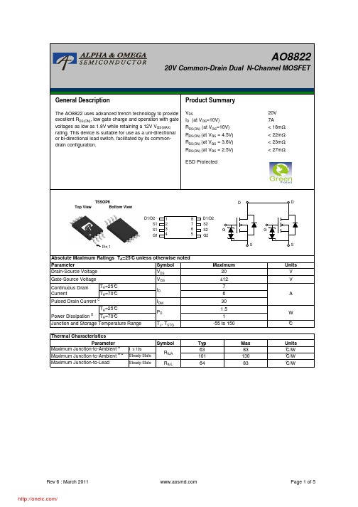
Symbolt ≤ 10s Steady-State Steady-StateR θJLW Maximum Junction-to-Lead°C/W°C/W Maximum Junction-to-Ambient A D 6413083Maximum Junction-to-Ambient A T A =25°C T A =70°C Power DissipationBPulsed Drain Current CContinuous Drain T A =25°C AV Units ParameterAbsolute Maximum Ratings T A =25°C unless otherwise notedV Gate-Source Voltage Drain-Source Voltage °C/W R θJA 6310183°CThermal Characteristics Units ParameterTyp Max T A =70°CJunction and Storage Temperature Range Pin 1DSSymbolMin Typ Max Units BV DSS 20VV DS =20V, V GS =0V1T J =55°C 5I GSS 10µA BV GSO ±12V V GS(th)Gate Threshold Voltage 0.50.81V I D(ON)30A 131518T J =125°C2227151722m Ω161823m Ω182127m Ω28m Ωg FS 31S V SD 0.71V I S2A C iss 520650780pF C oss 140pF C rss60pFQ g (10V)121518nC Q g (4.5V)56.78nC Q gs 3.6nC Q gd 3nC t D(on)0.25us t r 0.45us t D(off)11us t f 4ust rr 81012ns Q rr81113.5nCTHIS PRODUCT HAS BEEN DESIGNED AND QUALIFIED FOR THE CONSUMER MARKET. APPLICATIONS OR USES AS CRITICAL COMPONENTS IN LIFE SUPPORT DEVICES OR SYSTEMS ARE NOT AUTHORIZED. AOS DOES NOT ASSUME ANY LIABILITY ARISING OUT OF SUCH APPLICATIONS OR USES OF ITS PRODUCTS. AOS RESERVES THE RIGHT TO IMPROVE PRODUCT DESIGN,FUNCTIONS AND RELIABILITY WITHOUT NOTICE.Body Diode Reverse Recovery TimeDrain-Source Breakdown Voltage On state drain currentI D =250µA, V GS =0V V GS =10V, V DS =5V V GS =10V, I D =7AReverse Transfer CapacitanceI F =7A, dI/dt=500A/µsV GS =0V, V DS =10V, f=1MHzSWITCHING PARAMETERS Electrical Characteristics (T J =25°C unless otherwise noted)STATIC PARAMETERS ParameterConditions I DSS µA V DS =V GS I D =250µA V DS =0V, V GS = ±10V Zero Gate Voltage Drain Current Gate-Body leakage current Gate-Source Breakdown Voltage V DS =0V, I G =±250µA Forward Transconductance Diode Forward VoltageR DS(ON)Static Drain-Source On-Resistancem ΩI S =1A,V GS =0VV DS =5V, I D =7A V GS =1.8V, I D =2AV GS =4.5V, I D =6.6A V GS =3.6V, I D =6A V GS =2.5V, I D =5.5A Turn-Off Fall TimeTotal Gate Charge V GS =10V, V DS =10V, I D =7AGate Source Charge Gate Drain Charge Total Gate Charge Body Diode Reverse Recovery Charge I F =7A, dI/dt=500A/µsMaximum Body-Diode Continuous CurrentInput Capacitance Output CapacitanceTurn-On DelayTime DYNAMIC PARAMETERS Turn-On Rise Time Turn-Off DelayTime V GS =10V, V DS =10V, R L =1.5Ω,R GEN =3ΩA. The value of R θJA is measured with the device mounted on 1in 2FR-4 board with 2oz. Copper, in a still air environment with T A =25°C. The value in any given application depends on the user's specific board design.B. The power dissipation P D is based on T J(MAX)=150°C, using ≤ 10s junction-to-ambient thermal resistance.C. Repetitive rating, pulse width limited by junction temperature T J(MAX)=150°C. Ratings are based on low frequency and duty cycles to keep initialT J =25°C.D. The R θJA is the sum of the thermal impedence from junction to lead R θJL and lead to ambient.E. The static characteristics in Figures 1 to 6 are obtained using <300µs pulses, duty cycle 0.5% max.F. These curves are based on the junction-to-ambient thermal impedence which is measured with the device mounted on 1in 2 FR-4 board with 2oz. Copper, assuming a maximum junction temperature of T J(MAX)=150°C. The SOA curve provides a single pulse ratin g.TYPICAL ELECTRICAL AND THERMAL CHARACTERISTICSTYPICAL ELECTRICAL AND THERMAL CHARACTERISTICSQ g (nC)Figure 7: Gate-Charge CharacteristicsV G S (V o l t s )48121620V DS (Volts)Figure 8: Capacitance Characteristics C a p a c i t a n c e (p F )VdsCharge Gate Charge Test Circuit & WaveformD iode RVVddVddVR esistive S w itching Test C ircuit & W aveform s分销商库存信息: AOSAO8822。
SA50-11GWA中文资料

Internal
Circuit
Diagram
Notes:
1. All dimensions are in millimeters (inches), Tolerance is ±0.25(0.01")unless otherwise noted. 2. Specifications are subjected to change whitout notice.
High Efficiency Red
105 30 150 5
Super Bright Green
105 25 150 5
Yellow
105 30 150 5
Super Bright Red
100 30 150 5
Units
mW mA mA V
-40 °C To +85 °C 260 °C For 5 Seconds
21000
Description
Common Anode, Rt. Hand Decimal Common Cathode, Rt. Hand Decimal Common Anode, Rt. Hand Decimal Common Cathode, Rt. Hand Decimal Common Anode, Rt. Hand Decimal Common Cathode, Rt. Hand Decimal Common Anode, Rt. Hand Decimal Common Cathode, Rt. Hand Decimal
Typ.
625 565 590 660 45 30 35 20 12 45 10 95 2.0 2.2 2.1 1.85 10
Max.
Units
SNK088A-JWLD-E11-A01规格书
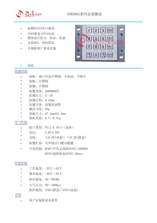
7 8 9 下翻
*
清除
0
确认
2、对应键值:
键位 码值
1
0x31
2
0x32
3
0x33
40x34Βιβλιοθήκη 50x356
0x36
7
0x37
8
0x38
3、接口类型:RS232串口
键位 9 0 点
清除 退出 上翻 下翻 确认
4、产品识别码:SNK088A-JWLD-E11-A01
码值 0x39 0x30 0x2e 0x08 0x1b 0x21 0x22 0x0d
所有尺寸单位均为毫米
尺寸公差为:
批准
X.X=±0.25 X.XX=±0.10
零件 材料
见BOM
角 度: X.X=± 0.50°
拔模角度:0.50°
零件
表 面 见技术要求
处理
表面粗糙度:
比 例 1 :1 数 量
深圳市旭子科技有限公司
零 件 安装尺寸图 视图
名称
方向
零 件 JWLD-E11-A01 图 A4
· 激活力度:50g · 面板尺寸:87.5mm*91.5mm · 整机重量:0.5~0.7kg 电气性能
· 接口类型:PS/2 & 串口(加密) · 电压: 5.0V±10% ·
功耗: ≤0.5W(动态),≤0.2W(静态) · · 按键扩展:可外接2片4键功能键
· 可靠性能:MTBF(平均无故障时间)>20000H
SNK088A系列金属键盘
· 标准RS232串口通讯 · IP65静态/IP54动态 · 整体设计防尘,防水,防暴 · 支持DES,3DES算法 · 可根据客户要求定制
· 规格
NCP702SN18T1G,NCP702SN28T1G,NCP702SN30T1G,NCP702SN33T1G, 规格书,Datasheet 资料

NCP702200 mA, Ultra-Low Quiescent Current, Ultra-Low Noise, LDO Linear Voltage RegulatorNoise sensitive applications such as Phase Locked Loops,Oscillators, Frequency Synthesizers, Low Noise Amplifiers and other Precision Instrumentation require very clean power supplies. The NCP702 is a 200 mA LDO that provides the engineer with a very stable, accurate voltage with ultra −low noise and very high Power Supply Rejection Ratio (PSRR), making it suitable for RF applications. The device doesn’t require an additional noise bypass capacitor to achieve ultra −low noise performance. In order to optimize performance for battery operated portable applications, the NCP702employs an Adaptive Ground Current feature for ultra −low ground current consumption during light −load conditions.Features•Operating Input V oltage Range: 2.0 V to 5.5 V•Available in Fixed V oltage Options: 0.8 to 3.5 V Contact Factory for Other V oltage Options •Output V oltage Trimming Step: 2.5 mV •Ultra −Low Quiescent Current of Typ. 10 m A•Ultra −Low Noise: 11 m V RMS from 100 Hz to 100 kHz •Very Low Dropout: 140 mV Typical at 200 mA •±2% Accuracy Over Full Load/Line/Temperature •High PSRR: 68 dB at 1 kHz•Thermal Shutdown and Current Limit Protections•Internal Soft −Start to Limit the Turn −On Inrush Current •Stable with a 1 m F Ceramic Output Capacitor•Available in TSOP −5 and XDFN 1.5 x 1.5 mm Package •Active Output Discharge for Fast Output Turn −Off •These are Pb −Free DevicesTypical Applicaitons•PDAs, Mobile Phones, GPS, Smartphones•Wireless Handsets, Wireless LAN, Bluetooth, Zigbee •Portable Medical Equipment•Other Battery Powered ApplicationsFigure 1. Typical Application SchematicSee detailed ordering and shipping information in the package dimensions section on page 18 of this data sheet.ORDERING INFORMATIONTSOP −5SN SUFFIXCASE 483X, XXX = Specific Device Code M= Date Code A = Assembly Location Y = YearW = Work Week G = Pb −Free Package15MARKING DIAGRAMSXDFN −6MX SUFFIXCASE 711AEX M G1PIN CONNECTIONS5−Pin TSOP −5(Top View)6−Pin XDFN 1.5 x 1.5 mm(Top View)OUTN/CN/C IN EN GND IN ENN/C OUT GNDFigure 2. Simplified Schematic Block DiagramINOUTGNDENTable 1. PIN FUNCTION DESCRIPTIONPin No.XDFN 6Pin No.TSOP −5Pin Name Description15OUT Regulated output voltage pin. A small 1 m F ceramic capacitor is needed from this pin to ground to assure stability.24N/C Not connected. This pin can be tied to ground to improve thermal dissipation.32GND Power supply ground.43EN Driving EN over 0.9 V turns on the regulator. Driving EN below 0.4 V puts the regulator into shutdown mode.5N/C Not connected. This pin can be tied to ground to improve thermal dissipation.61INInput pin. It is recommended to connect a 1 m F ceramic capacitor close to the device pin.Table 2. ABSOLUTE MAXIMUM RATINGSRatingSymbol Value Unit Input Voltage (Note 1)V IN −0.3 V to 6 V V Output Voltage V OUT −0.3 V to V IN + 0.3 V V Enable InputV EN −0.3 V to V IN + 0.3 VV Output Short Circuit Duration t SC Indefinite s Maximum Junction Temperature T J(MAX)125°C Storage TemperatureT STG −55 to 150°C ESD Capability, Human Body Model (Note 2)ESD HBM 2000V ESD Capability, Machine Model (Note 2)ESD MM200VStresses exceeding Maximum Ratings may damage the device. Maximum Ratings are stress ratings only. Functional operation above the Recommended Operating Conditions is not implied. Extended exposure to stresses above the Recommended Operating Conditions may affect device reliability.1.Refer to ELECTRICAL CHARACTERISTICS and APPLICATION INFORMATION for Safe Operating Area.2.This device series incorporates ESD protection and is tested by the following methods:ESD Human Body Model tested per AEC −Q100−002 (EIA/JESD22−A114)ESD Machine Model tested per AEC −Q100−003 (EIA/JESD22−A115)Latchup Current Maximum Rating tested per JEDEC standard: JESD78.Table 3. THERMAL CHARACTERISTICS (Note 3)Rating Symbol Value UnitThermal Characteristics, TSOP−5,Thermal Resistance, Junction−to−AirThermal Characterization Parameter, Junction−to−Lead (Pin 2)q JAy JA224115°C/WThermal Characteristics, XDFN6 1.5 x 1.5 mmThermal Resistance, Junction−to−AirThermal Characterization Parameter, Junction−to−Board q JAy JB14981°C/W3.Single component mounted on 1 oz, FR4 PCB with 645 mm2 Cu area.Table 4. ELECTRICAL CHARACTERISTICS−40°C ≤ T J≤ 125°C; V IN = V OUT(NOM) + 0.3 V or 2.0 V, whichever is greater; V EN = 0.9 V, I OUT = 10 mA, C IN = C OUT = 1 m F.Typical values are at T J = +25°C. Min/Max values are specified for T J = −40°C and T J = 125°C respectively. (Note 4) Parameter Test Conditions Symbol Min Typ Max Unit Operating Input Voltage V IN 2.0 5.5V Undervoltage lock−out V IN rising UVLO 1.2 1.6 1.9V Output Voltage Accuracy V OUT + 0.3 V ≤ V IN≤ 5.5 V, I OUT = 0 − 200 mA V OUT−2+2% Line Regulation V OUT + 0.3 V ≤ V IN≤ 4.5 V, I OUT = 10 mA Reg LINE290m V/VV OUT + 0.3 V ≤ V IN≤ 5.5 V, I OUT = 10 mA Reg LINE440m V/V Load Regulation I OUT = 0 mA to 200 mA Reg LOAD13m V/mA Dropout voltage (Note 5) I OUT = 200 mA, V OUT(nom) = 2.5 V V DO140200mV Output Current Limit V OUT = 90% V OUT(nom)I CL220385550mA Quiescent current I OUT = 0 mA I Q1016m A Ground current I OUT = 2 mA I GND60m AI OUT = 200 mA I GND160m A Shutdown current (Note 6) V EN≤ 0.4 V I DIS0.005m AV EN≤ 0.4 V, V IN = 4.5 V I DIS0.011m A EN Pin Threshold VoltageHigh Threshold Low Threshold V EN Voltage increasingV EN Voltage decreasingV EN_HIV EN_LO0.90.4VEN Pin Input Current V EN = V IN = 5.5 V I EN110500nA Turn−On Time (Note 7) C OUT = 1.0 m F, I OUT = 1 mA t ON300m s Output Voltage Overshoot onStart−up (Note 8)V EN = 0 V to 0.9 V, 0 ≤ I OUT≤ 200 mA D V OUT2%Load Transient I OUT = 1 mA to 200 mA orI OUT = 200 mA to 1 mA in 10 m s, C OUT = 1 m FD V OUT−30/+30mVPower Supply Rejection Ratio V IN = 3 V, V OUT = 2.5 VI OUT = 150 mA f = 100 Hzf = 1 kHzf = 10 kHzPSRR706853dBOutput Noise Voltage V OUT = 2.5 V, V IN = 3 V, I OUT = 200 mAf = 100 Hz to 100 kHzV N11m V rms Active Discharge Resistance V EN < 0.4 V R DIS1k WThermal Shutdown Temperature Temperature increasing from T J = +25°C T SD160°CThermal Shutdown Hysteresis Temperature falling from T SD T SDH−20−°C 4.Performance guaranteed over the indicated operating temperature range by design and/or characterization. Production tested at T J = T A= 25_C. Low duty cycle pulse techniques are used during testing to maintain the junction temperature as close to ambient as possible.5.Characterized when V OUT falls 100 mV below the regulated voltage at V IN = V OUT(NOM)+ 0.3 V.6.Shutdown Current is the current flowing into the IN pin when the device is in the disable state.7.Turn−On time is measured from the assertion of EN pin to the point when the output voltage reaches 0.98 V OUT(NOM)8.Guaranteed by design.Figure 3. Output Voltage Noise Spectral Density for V OUT = 0.8 V, C OUT = 1 m FFREQUENCY (Hz)Figure 4. Output Voltage Noise Spectral Density for V OUT = 0.8 V, C OUT = 4.7 m FFigure 5. Output Voltage Noise Spectral Density for V OUT = 0.8 V, C OUT = 10 m FO U T P U T V O L T A G E N O I S E (m V /r t H z )1 mA 21.7421.1710 mA14.6214.07200 mA10.7410.0210 Hz − 100 kHz100 Hz − 100 kHzRMS Output NoiseI OUT FREQUENCY (Hz)O U T P U T V O L T A G E N O I S E (m V /r t H z )1 mA 14.1613.4310 mA 14.2013.70200 mA10.9910.4810 Hz − 100 kHz100 Hz − 100 kHzRMS Output NoiseI OUT FREQUENCY (Hz)O U T P U T V O L T A G E N O I S E (m V /r t H z )1 mA 12.9412.1110 mA 12.7812.25200 mA11.3310.8310 Hz − 100 kHz100 Hz − 100 kHzRMS Output NoiseI OUTFigure 6. Output Voltage Noise Spectral Density for V OUT = 3.3 V, C OUT = 1 m FFREQUENCY (Hz)Figure 7. Output Voltage Noise Spectral Density for V OUT = 3.3 V, C OUT = 4.7 m FFigure 8. Output Voltage Noise Spectral Density for V OUT = 3.3 V, C OUT = 10 m FO U T P U T V O L T A G E N O I S E (m V /r t H z)1 mA 20.2817.8710 mA 16.7313.90200 mA13.7010.2110 Hz − 100 kHz100 Hz − 100 kHzRMS Output NoiseI OUT FREQUENCY (Hz)O U T P U T V O L T A G E N O I S E (m V /r t H z )1 mA 15.7611.8210 mA 17.0913.88200 mA14.5111.4710 Hz − 100 kHz100 Hz − 100 kHzRMS Output NoiseI OUT FREQUENCY (Hz)O U T P U T V O L T A G E N O I S E (m V /r t H z )1 mA 14.8710.5710 mA 16.0012.65200 mA14.8911.8410 Hz − 100 kHz100 Hz − 100 kHzRMS Output NoiseI OUTFigure 9. Power Supply Rejection Ratio,V OUT = 0.8 V, C OUT = 1 m FFigure 10. Power Supply Rejection Ratio,V OUT = 0.8 V, C OUT = 4.7 m FFREQUENCY (Hz)FREQUENCY (Hz)Figure 11. Power Supply Rejection Ratio,V OUT = 3.3 V, C OUT = 1 m FFigure 12. Power Supply Rejection Ratio,V OUT = 3.3 V, COUT = 4.7 m FFREQUENCY (Hz)FREQUENCY (Hz)Figure 13. Power Supply Rejection Ratio,V OUT = 3.3 V, COUT = 10 m F Figure 14. PSRR vs. Voltage Differential,C OUT = 4.7 m F, I OUT= 200 mAFREQUENCY (Hz)V IN − V OUT VOLTAGE DIFFERENTIAL (V)010304050608090P S R R (d B )P S R R (d B )P S R R (d B )P S R R (d B )P S R R (d B )P S R R (d B )2070Figure 15. PSRR vs. Voltage Differential,C OUT = 4.7 m F, I OUT = 10 mAFigure 16. Quiescent Current vs. Input Voltage,V OUT = 3.3 VV IN − V OUT VOLTAGE DIFFERENTIAL (V)V IN , INPUT VOLTAGE (V)Figure 17. Quiescent Current vs. Input Voltage,V OUT = 0.8 VFigure 18. Dropout Voltage vs. Output Current,V OUT = 3.3 VV IN , INPUT VOLTAGE (V)I OUT , OUTPUT CURRENT (mA)Figure 19. Dropout Voltage vs. Output Current,V OUT = 2.5 V Figure 20. Output Voltage vs. Temperature,V OUT = 0.8 VI OUT , OUTPUT CURRENT (mA)T J , JUNCTION TEMPERATURE (°C)P S R R (d B )I Q , Q U I E S C E N T C U R R E N T (m A )I Q , Q U I E S C E N T C U R R E N T (m A )V D R O P , D R O P O U T V O L T A G E (m V )V D R O P , D R O P O U T V O L T A G E (m V )V O U T , O U T P U T V O L T A G E (V )Figure 21. Output Voltage vs. Temperature,V OUT = 1.8 VFigure 22. Output Voltage vs. Temperature,V OUT = 3.3 VT J , JUNCTION TEMPERATURE (°C)T J , JUNCTION TEMPERATURE (°C)Figure 23. Load Regulation vs. Temperature,V OUT = 0.8 VFigure 24. Load Regulation vs. Temperature,V OUT = 1.8 VT J , JUNCTION TEMPERATURE (°C)T J , JUNCTION TEMPERATURE (°C)Figure 25. Load Regulation vs. Temperature,V OUT = 3.3 V Figure 26. Line Regulation vs. Temperature,V OUT = 0.8 VT J , JUNCTION TEMPERATURE (°C)T J , JUNCTION TEMPERATURE (°C)V O U T , O U T P U T V O L T A G E (V )V O U T , O U T P U T V O L T A G E (V )R E G L O A D , L O A D R E G U L A T I O N (m V )R E G L I N E , L I N E R E G U L A T I O N (m V /V )3.2853.2893.2933.3013.3093.3133.2973.3053.317R E G L O A D , L O A D R E G U L A T I O N (m V )R E G L O A D , L O A D R E G U L A T I O N (m V )Figure 27. Line Regulation vs. Temperature,V OUT = 1.8 VFigure 28. Line Regulation vs. Temperature,V OUT = 3.3 VT J , JUNCTION TEMPERATURE (°C)T J , JUNCTION TEMPERATURE (°C)Figure 29. Disable Current vs. Temperature,V OUT = 1.8 VFigure 30. Disable Current vs. Temperature,V OUT = 3.3 VT J , JUNCTION TEMPERATURE (°C)T J , JUNCTION TEMPERATURE (°C)−Figure 31. Disable Current vs. Temperature,V OUT = 0.8 V Figure 32. Output Current Limit vs.Temperature, V OUT = 0.8 VT J , JUNCTION TEMPERATURE (°C)T J , JUNCTION TEMPERATURE (°C)R E G L I N E , L I N E R E G U L A T I O N (m V /V )I D I S , D I S A B L E C U R R E N T (m A )I D I S , D I S A B L E C U R R E N T (m A )I O U T , O U T P U T C U R R E N T (m A )R E G L I N E , L I N E R E G U L A T I O N (m V /V )−0I D I S , D I S A B L E C U R R E N T (m A )−250270290310330350370390410430450Figure 33. Output Current Limit vs.Temperature, V OUT = 3.3 VFigure 34. Enable Low Threshold VoltageT J , JUNCTION TEMPERATURE (°C)T J , JUNCTION TEMPERATURE (°C)Figure 35. Enable High Threshold VoltageFigure 36. Enable Turn −On Response,V OUT = 3.3 V, C OUT = 1 m FT J , JUNCTION TEMPERATURE (°C)Figure 37. Enable Turn −On Response,V OUT = 3.3 V, C OUT = 3 m F Figure 38. Enable Turn −On Response,V OUT = 0.8 V, C OUT = 1 m FI O U T , O U T P U T C U R R E N T (m A )V E N _H I , E N H I G H T H R E S H O L D (V )V E N _L O W , E N L O W T H R E S H O L D (V )V IN = 3.6 VV OUT(nom) = 3.3 V C OUT = 1 m F C IN = none I OUT = 1 mA T A = 25°COUTENI INRUSH I INRUSH = 60 mA100 m s/div1 V /d i v1 V /d i v50 m A /d i vI INRUSH = 115 mAV IN = 3.6 VV OUT(nom) = 3.3 V C OUT = 3 m F C IN = none I OUT = 1 mA T A = 25°COUTENI INRUSH1 V /d i v1 V /d i v50 m A /d i v0.5 V /d i v1 V /d i vV IN = 2.0 VV OUT(nom) = 0.8 V C OUT = 1 m F C IN = none I OUT = 1 mA T A = 25°C50 m A /d i v100 m s/div I INRUSH = 20 mA100 m s/divFigure 39. Enable Turn −On Response,V OUT = 0.8 V, C OUT = 3 m F0.5 V /d i v1 V /d i vV IN = 2.0 VV OUT(nom) = 0.8 V C OUT = 3 m F C IN = none I OUT = 1 mA T A = 25°C50 m A /d i vI INRUSH = 45 mA100 m s/div11.522.533.544.55C OUT , OUTPUT CAPACITANCE (m F)I I N R U S H , I N R U S H C U R R E N T (m A )Figure 40. Turn −On Inrush Current vs. OutputCapacitanceFigure 41. Enable Turn −Off Response,V OUT = 3.3 V, C OUT = 1 m F Figure 42. Enable Turn −Off Response,V OUT = 3.3 V, C OUT = 4.7 m FFigure 43. Enable Turn −Off Response,V OUT = 3.3 V, C OUT = 10 m F Figure 44. Slow Input Voltage Turn −On/Turn −Off, V OUT = 3.3 VFigure 45. Line Transient Response −Rising Edge, V OUT = 3.3 V Figure 46. Line Transient Response −Falling Edge, V OUT = 3.3 VFigure 47. Load Transient Response − Rising Edge, I OUT = 1 mA − 200 mA, V OUT = 0.8 V Figure 48. Load Transient Response − Falling Edge, I OUT = 1 mA − 200 mA, V OUT = 0.8 VFigure 49. Load Transient Response − Rising Edge, I OUT = 1 mA − 200 mA, C OUT = 1.0 m F Figure 50. Load Transient Response − Falling Edge, I OUT = 1 mA − 200 mA, C OUT = 1.0 m FFigure 51. Load Transient Response − Rising Edge, I OUT = 1 mA − 200 mA, C OUT = 4.7 m F Figure 52. Load Transient Response − Falling Edge, I OUT = 1 mA − 200 mA, C OUT = 4.7 m FFigure 53. Load Transient Response − Rising Edge, I OUT = 1 mA − 200 mA, C OUT = 10 m F Figure 54. Load Transient Response − Falling Edge, I OUT = 1 mA − 200 mA, C OUT = 10 m FFigure 55. Output Short Circuit ResponseFigure 56. Cycling between Output ShortCircuit and Thermal ShutdownFigure 57. Ground Current vs. Output Current,I OUT = 0 mA to 5 mA Figure 58. Ground Current vs. Output Current,I= 0 mA to 200 mAI OUT, OUTPUT CURRENT (mA)I OUT, OUTPUT CURRENT (mA)IGND,GROUNDCURRENT(mA)IGND,GROUNDCURRENT(mA)1020304050607080Figure 59. EN Pin Input Current vs. Enable PinVoltageFigure 60. Output Capacitor ESR vs. OutputCurrentV EN, ENABLE VOLTAGE (V)I OUT, OUTPUT CURRENT (mA)IEN,ENPININPUTCURRENT(mA)ESR(W)GeneralThe NCP702 is a high performance 200 mA Low Dropout Linear Regulator. This device delivers excellent noise and dynamic performance.Thanks to its adaptive ground current feature the device consumes only 10 m A of quiescent current at no−load condition.The regulator features ultra−low noise of 11 m V RMS, PSRR of 68 dB at 1 kHz and very good load/line transient performance. Such excellent dynamic parameters and small package size make the device an ideal choice for powering the precision analog and noise sensitive circuitry in portable applications. The LDO achieves this ultra low noise level output without the need for a noise bypass capacitor.A logic EN input provides ON/OFF control of the output voltage. When the EN is low the device consumes as low as typ. 10 nA from the IN pin.The LDO achieves ultra−low output voltage noise without the need for additional noise bypass capacitor.The device is fully protected in case of output overload, output short circuit condition and overheating, assuring a very robust design.Input Capacitor Selection (C IN)It is recommended to connect a minimum of 1 m F Ceramic X5R or X7R capacitor close to the IN pin of the device. This capacitor will provide a low impedance path for unwanted AC signals or noise modulated onto constant input voltage. There is no requirement for the min./max. ESR of the input capacitor but it is recommended to use ceramic capacitors for their low ESR and ESL. A good input capacitor will limit the influence of input trace inductance and source resistance during sudden load current changes. Larger input capacitor may be necessary if fast and large load transients are encountered in the application. Output Decoupling (C OUT)The NCP702 is designed to be stable with a small 1.0m F ceramic capacitor on the output. To assure proper operation it is strongly recommended to use min. 1.0 m F capacitor with the initial tolerance of ±10%, made of X7R or X5R dielectric material types.There is no requirement for the minimum value of Equivalent Series Resistance (ESR) for the C OUT but the maximum value of ESR should be less than 700 m W. Larger output capacitors could be used to improve the load transient response or high frequency PSRR as shown in typical characteristics. The initial tolerance requirements can be wider than ±10% when using capacitors larger than 1m F.It is not recommended to use tantalum capacitors on the output due to their large ESR. The equivalent series resistance of tantalum capacitors is also strongly dependent on the temperature, increasing at low temperature. The tantalum capacitors are generally more costly than ceramic capacitors.The table on this page lists the capacitors which were used during the IC evaluation.No−load OperationThe regulator remains stable and regulates the output voltage properly within the ±2% tolerance limits even with no external load applied to the output.2 V ... 5.5 V0 mA ... 200 mAFigure 61. Typical Applications SchematicsLIST OF CAPACITORS USED DURING THE NCP702 EVALUATION:Symbol Manufacturer Part Number DescriptionC1, C2Kemet C0402C105K8PACTU 1 m F Ceramic ±10%, 10 V, 0402, X5R TDK C1005X5R1A105K−||−Murata GRM155R61A105KE15D−||−AVX0402ZD105KAT2A−||−Multicomp MCCA000571 1 m F Ceramic ±10%, 50 V, 1206, X7R Panason − ECG ECJ−0EB0J475M 4.7 m F Ceramic ±20%, 6.3 V, 0402, X5REnable OperationThe NCP702 uses the EN pin to enable/disable its output and to deactivate/activate the active discharge function.If the EN pin voltage is <0.4 V the device is guaranteed to be disabled. The pass transistor is turned −off so that there is virtually no current flow between the IN and OUT. The active discharge transistor is active so that the output voltage V OUT is pulled to GND through a 1 k W resistor. In the disable state the device consumes as low as typ. 10 nA from the V IN .If the EN pin voltage >0.9 V the device is guaranteed to be enabled. The NCP702 regulates the output voltage and the active discharge transistor is turned −off.The EN pin has internal pull −down current source with typ. value of 110 nA which assures that the device is turned −off when the EN pin is not connected. A build in 2mV of hysteresis in the EN prevents from periodic on/off oscillations that can occur due to noise.In the case where the EN function isn’t required the EN pin should be tied directly to IN.Undervoltage LockoutThe internal UVLO circuitry assures that the device becomes disabled when the V IN falls below typ. 1.5 V . When the V IN voltage ramps −up the NCP702 becomes enabled, if V IN rises above typ. 1.6 V . The 100 mV hysteresis prevents on/off oscillations that can occur due to noise on V IN line.Reverse CurrentThe PMOS pass transistor has an inherent body diode which will be forward biased in the case that V OUT > V IN .Due to this fact in cases where the extended reverse current condition is anticipated the device may require additional external protection.Output Current LimitOutput Current is internally limited within the IC to a typical 380 mA. The NCP702 will source this amount ofcurrent measured with the output voltage 100 mV lower than the nominal V OUT . If the Output V oltage is directly shorted to ground (V OUT = 0 V), the short circuit protection will limit the output current to 390 mA (typ). The current limit and short circuit protection will work properly up to V IN =5.5V at T A = 25°C. There is no limitation for the short circuit duration.Thermal ShutdownWhen the die temperature exceeds the Thermal Shutdown threshold (T SD − 160°C typical), Thermal Shutdown event is detected and the device is disabled. The IC will remain in this state until the die temperature decreases below the Thermal Shutdown Reset threshold (T SDU − 140°C typical).Once the IC temperature falls below the 140°C the LDO is enabled again. The thermal shutdown feature provides protection from a catastrophic device failure due to accidental overheating. This protection is not intended to be used as a substitute for proper heat sinking.Power DissipationAs power dissipated in the NCP702 increases, it might become necessary to provide some thermal relief. The maximum power dissipation supported by the device is dependent upon board design and layout. Mounting pad configuration on the PCB, the board material, and the ambient temperature affect the rate of junction temperature rise for the part.The maximum power dissipation the NCP702 can handle is given by:P D(MAX)+ƪT J(MAX)*T A ƫq JA(eq. 1)The power dissipated by the NCP702 for given application conditions can be calculated from the following equations:P D [V IN ǒI GND @I OUT Ǔ)I OUT ǒV IN *V OUT Ǔ(eq. 2)Figure 62. q JA and P D(MAX) vs. Copper Area (TSOP5)PCB COPPER AREA (mm 2)q J A , J U N C T I O N T O A M B I E N T T H E R M A L R E S I S T A N C E (°C /W )0.200.250.300.400.450.500.600.650.350.55P D (M A X ), M A X I M U M P O W E R D I S S I P A T I O N (W )Figure 63. q JA and P D(MAX) vs. Copper Area (XDFN6)PCB COPPER AREA (mm 2)q J A , J U N C T I O N T O A M B I E N T T H E R M A L R E S I S T A N C E (°C /W )0.10.20.30.50.70.80.40.6P D (M A X ), M A X I M U M P O W E R D I S S I P A T I O N (W )Load RegulationThe NCP702 features very good load regulation of maximum 2.6 mV in the 0 mA to 200 mA range. In order to achieve this very good load regulation a special attention to PCB design is necessary. The trace resistance from the OUT pin to the point of load can easily approach 100 m Ω which will cause a 20 mV voltage drop at full load current,deteriorating the excellent load regulation.Line RegulationThe IC features very good line regulation of 0.44mV/V measured from V IN = V OUT + 0.3 V to 5.5 V . For battery operated applications it may be important that the line regulation from V IN = V OUT + 0.3 V up to 4.5 V is only 0.29mV/V.Power Supply Rejection RatioThe NCP702 features very good Power Supply Rejection ratio. If desired the PSRR at higher frequencies in the range 100kHz – 10 MHz can be tuned by the selection of C OUT capacitor and proper PCB layout.Output NoiseThe IC is designed for ultra −low noise output voltage.Figures 3 – 8 illustrate the noise performance for different V OUT , I OUT , C OUT . Generally the noise performance in the indicated frequency range improves with increasing output current, although even at I OUT = 1 mA the noise levels are below 22 m V RMS .Turn −On TimeThe turn −on time is defined as the time period from EN assertion to the point in which V OUT will reach 98% of its nominal value. This time is dependent on V OUT(NOM),C OUT , T A . The turn −on time temperature dependence is shown below:Figure 64. Turn −On Time vs. TemperatureT J , JUNCTION TEMPERATURE (°C)E N , T U R N −O N T I M E (m s )Internal SoftStartThe Internal Soft −Start circuitry will limit the inrush current during the LDO turn-on phase. Please refer to Figure 43 for typical inrush current values for given output capacitance.The soft −start function prevents from any output voltage overshoots and assures monotonic ramp-up of the output voltage.PCB Layout RecommendationsTo obtain good transient performance and good regulation characteristics place C IN and C OUT capacitors close to the device pins and make the PCB traces wide. In order to minimize the solution size use 0402 capacitors. Larger copper area connected to the pins will also improve the device thermal resistance. The actual power dissipation can be calculated by the formula given in Equation 2.ORDERING INFORMATIONDeviceVoltage OptionMarkingPackageShipping †NCP702MX18TCG 1.8 V P XDFN63000 / Tape & ReelNCP702MX28TCG 2.8 V 2NCP702MX30TCG 3.0 V 3NCP702MX33TCG 3.3 V 4NCP702SN18T1G 1.8 V A7J TSOP53000 / Tape & ReelNCP702SN28T1G 2.8 V AD2NCP702SN30T1G 3.0 V A7R NCP702SN33T1G3.3 VA7T†For information on tape and reel specifications, including part orientation and tape sizes, please refer to our Tape and Reel Packaging Specifications Brochure, BRD8011/D.NOTES:1.DIMENSIONING AND TOLERANCING PER ASME Y14.5M, 1994.2.CONTROLLING DIMENSION: MILLIMETERS.3.DIMENSION b APPLIES TO PLATEDTERMINAL AND IS MEASURED BETWEEN0.10 AND 0.20mm FROM TERMINAL TIP.2XXDFN6 1.5x1.5, 0.5P CASE 711AE −01ISSUE ODIM A MIN MAX MILLIMETERS 0.350.45A10.000.05A30.13 REF b 0.200.30D E e L MOUNTING FOOTPRINT*L1 1.50 BSC 1.50 BSC 0.50 BSC 0.400.60---0.15DIMENSIONS: MILLIMETERS0.735X*For additional information on our Pb −Free strategy and soldering details, please download the ON Semiconductor Soldering and Mounting Techniques Reference Manual, SOLDERRM/D.L1DETAIL ALALTERNATE TERMINAL CONSTRUCTIONSDETAIL BALTERNATE CONSTRUCTIONSL20.500.70RECOMMENDEDTSOP −5CASE 483−02ISSUE HNOTES:1.DIMENSIONING AND TOLERANCING PER ASME Y14.5M, 1994.2.CONTROLLING DIMENSION: MILLIMETERS.3.MAXIMUM LEAD THICKNESS INCLUDES LEAD FINISH THICKNESS. MINIMUM LEAD THICKNESS IS THE MINIMUM THICKNESS OF BASE MATERIAL.4.DIMENSIONS A AND B DO NOT INCLUDE MOLD FLASH, PROTRUSIONS, OR GATE BURRS.5.OPTIONAL CONSTRUCTION: ANADDITIONAL TRIMMED LEAD IS ALLOWED IN THIS LOCATION. TRIMMED LEAD NOT TO EXTEND MORE THAN 0.2 FROM BODY .DIM MIN MAX MILLIMETERS A 3.00 BSC B 1.50 BSC C 0.90 1.10D 0.250.50G 0.95 BSC H 0.010.10J 0.100.26K 0.200.60L 1.25 1.55M 0 10 S2.503.00__ǒmm inchesǓ*For additional information on our Pb −Free strategy and solderingdetails, please download the ON Semiconductor Soldering and Mounting Techniques Reference Manual, SOLDERRM/D.SOLDERING FOOTPRINT*2X2XDETAIL ZON Semiconductor and are registered trademarks of Semiconductor Components Industries, LLC (SCILLC). SCILLC reserves the right to make changes without further notice to any products herein. SCILLC makes no warranty, representation or guarantee regarding the suitability of its products for any particular purpose, nor does SCILLC assume any liability arising out of the application or use of any product or circuit, and specifically disclaims any and all liability, including without limitation special, consequential or incidental damages.“Typical” parameters which may be provided in SCILLC data sheets and/or specifications can and do vary in different applications and actual performance may vary over time. All operating parameters, including “Typicals” must be validated for each customer application by customer’s technical experts. SCILLC does not convey any license under its patent rights nor the rights of others. SCILLC products are not designed, intended, or authorized for use as components in systems intended for surgical implant into the body, or other applications intended to support or sustain life, or for any other application in which the failure of the SCILLC product could create a situation where personal injury or death may occur. Should Buyer purchase or use SCILLC products for any such unintended or unauthorized application, Buyer shall indemnify and hold SCILLC and its officers, employees, subsidiaries, affiliates,and distributors harmless against all claims, costs, damages, and expenses, and reasonable attorney fees arising out of, directly or indirectly, any claim of personal injury or death associated with such unintended or unauthorized use, even if such claim alleges that SCILLC was negligent regarding the design or manufacture of the part. SCILLC is an Equal Opportunity/Affirmative Action Employer. This literature is subject to all applicable copyright laws and is not for resale in any manner.PUBLICATION ORDERING INFORMATION。
NCP1579DR2G,NCP1579DR2G,NCP1579DR2G, 规格书,Datasheet 资料

NCP1579Low Voltage Synchronous Buck ControllerThe NCP1579 is a low cost PWM controller designed to operate from a 5 V or 12 V supply. This device is capable of producing an output voltage as low as 0.8 V. This 8−pin device provides an optimal level of integration to reduce size and cost of the power supply. The NCP1579 provides a 1 A gate driver design and an internally set 275 kHz oscillator. In addition to the 1 A gate drive capability, other efficiency enhancing features of the gate driver include adaptivenon−overlap circuitry. The device also incorporates an externally compensated error amplifier and a capacitor programmable soft−start function. Protection features include programmable short circuit protection and undervoltage lockout (UVLO). The NCP1579 comes in an 8−pin SOIC package.Features•Input V oltage Range from 4.5 to 13.2 V•275 kHz Internal Oscillator•Boost Pin Operates to 30 V•V oltage Mode PWM Control•0.8 V ±2.0 % Internal Reference V oltage•Adjustable Output V oltage•Capacitor Programmable Soft−Start•Internal 1 A Gate Drivers•80% Max Duty Cycle•Input Under V oltage Lockout•Programmable Current Limit•These Devices are Pb−Free, Halogen Free/BFR Free and are RoHS CompliantApplications•STB•Blue−Ray DVD•LCD_TV•DSP & FPGA Power Supply•DC−DC Regulator ModulesSOIC−8D SUFFIXCASE 751MARKING DIAGRAMPIN CONNECTIONS1579= Specific Device CodeA= Assembly LocationL= Wafer LotY= YearW= Work WeekG= Pb−Free DeviceBST PHASETGGNDBGCOMP/DISFBVCC(Top View)Device Package Shipping†ORDERING INFORMATIONNCP1579DR2G SOIC−8(Pb−Free)2500/T ape & Reel†For information on tape and reel specifications, including part orientation and tape sizes, please refer to our T ape and Reel Packaging Specifications Brochure, BRD8011/D.Figure 1. Typical Application DiagramsFigure 2. Detailed Block DiagramCCR setPIN FUNCTION DESCRIPTIONPin No.Symbol Description1BST Supply rail for the floating top gate driver. To form a boost circuit, use an external diode to bring thedesired input voltage to this pin (cathode connected to BST pin). Connect a capacitor (C BST) between this pinand the PHASE pin. Typical values for C BST range from 0.1 m F to 1 m F. Ensure that C BST is placed near the IC.2TG Top gate MOSFET driver pin. Connect this pin to the gate of the top N−Channel MOSFET.3GND IC ground reference. All control circuits are referenced to this pin.4BG Bottom gate MOSFET driver pin. Connect this pin to the gate of the bottom N−Channel MOSFET.5V CC Supply rail for the internal circuitry. Operating supply range is 4.5 V to 13.2 V. Decouple with a 1 m Fcapacitor to GND. Ensure that this decoupling capacitor is placed near the IC.6FB This pin is the inverting input to the error amplifier. Use this pin in conjunction with the COMP pin tocompensate the voltage−control feedback loop. Connect this pin to the output resistor divider (if used) or dir-ectly to V out.7COMP/DIS Compensation Pin. This is the output of the error amplifier (EA) and the non−inverting input of the PWM com-parator. Use this pin in conjunction with the FB pin to compensate the voltage−control feedback loop. The com-pensation capacitor also acts as a soft−start capacitor. Pull this pin low for disable.8PHASE Switch node pin. This is the reference for the floating top gate driver. Connect this pin to the source of the top MOSFET.ABSOLUTE MAXIMUM RATINGSPin Name Symbol V MAX V MINMain Supply Voltage Input V CC15 V−0.3 V Bootstrap Supply Voltage Input BST30 V wrt/GND15 V wrt/PHASE35 V wrt/GND for < 50ns−0.3 VSwitching Node (Bootstrap Supply Return)PHASE26 V−0.7 V−5.0 V for < 50 nsHigh−Side Driver Output (Top Gate)TG30 V wrt/GND15 V wrt/PHASE−0.3 V wrt/PHASELow−Side Driver Output (Bottom Gate)BG15 V−0.3 V−2.0 V for < 200 ns Feedback FB 5.5 V−0.3 VCOMP/DISABLE COMP/DIS 5.5 V−0.3 VMAXIMUM RATINGSRating Symbol Value Unit Thermal Resistance, Junction−to−Ambient R q JA165°C/W Thermal Resistance, Junction−to−Case R q JC45°C/W Operating Junction Temperature Range T J0 to 125°C Operating Ambient Temperature Range T A0 to 70°C Storage Temperature Range T stg−55 to +150°C Lead Temperature Soldering (10 sec): Reflow (SMD styles only) Pb−Free260°C Moisture Sensitivity Level MSL3−Stresses exceeding Maximum Ratings may damage the device. Maximum Ratings are stress ratings only. Functional operation above the Recommended Operating Conditions is not implied. Extended exposure to stresses above the Recommended Operating Conditions may affect device reliability.ELECTRICAL CHARACTERISTICS (0_C < T A< 70_C; 4.5 V < V CC< 13.2 V, 4.5 V < [BST−PHASE]< 13.2 V, 4.5 V < BST < 30 V, 0 V < PHASE < 21 V, C TG= C BG= 1.0 nF, for min/max values unless otherwise noted.)Characteristic Conditions Min Typ Max Unit Input Voltage Range− 4.5−13.2V Boost Voltage Range− 4.5−26.5V Supply CurrentQuiescent Supply Current V FB = 1.0 V, No Switching, V CC= 13.2 V 1.0−8.0mA Boost Quiescent Current V FB = 1.0 V, No Switching, V CC = 13.2 V0.1− 1.0mA Under Voltage LockoutUVLO Threshold V CC Rising Edge 3.8− 4.2V UVLO Hysteresis−300370440mV Switching RegulatorVFB Feedback Voltage,Control Loop in RegulationT A = 0 to 70°C784800816mV Oscillator Frequency T A = 0 to 70°C233275317kHz Ramp−Amplitude Voltage0.8 1.1 1.4V Minimum Duty Cycle0−−% Maximum Duty Cycle707580% Error Amplifier (GM)Transconductance 3.0− 4.4mmho Open Loop DC Gain5570−DBOutput Source Current Output Sink Current V FB < 0.8 VV FB > 0.8 V8080120120−−m AInput Bias Current−0.1 1.0m A Soft−StartSS Source Current V FB < 0.8 V7.0−14m A Switch Over Threshold V FB = 0.8 V−100−% of Vref Gate DriversUpper Gate SourceV CC = 12 V, VTG = VBG = 2.0 V − 1.0−AUpper Gate Sink− 1.0−A Lower Gate Source− 1.0−A Lower Gate Sink− 2.0−A TG Falling to BG Rising Delay V CC = 12 V, TG < 2.0 V, BG > 2.0 V−4090ns BG Falling to TG Rising Delay V CC = 12 V, BG < 2.0 V, TG > 2.0 V−3590ns Enable Threshold0.30.40.5V Over−Current ProtectionOCSET Current Source Sourced from BG pin, before SS−10−m A OC Switch−Over Threshold−700−mV Fixed OC Threshold−−375−mVTYPICAL CHARACTERISTICS (T A = 25°C unless otherwise noted)Figure 3. I CC vs. TemperatureFigure 4. Oscillator Frequency (F SW ) vs.TemperatureT J , JUNCTION TEMPERATURE (°C)T J , JUNCTION TEMPERATURE (°C)7060504030201003.53.84.14.44.75.0Figure 5. Soft Start Sourcing Current vs.TemperatureFigure 6. SCP Threshold vs. TemperatureT J , JUNCTION TEMPERATURE (°C)T J , JUNCTION TEMPERATURE (°C)706050403020100891011121314706050403020100325335345355365375Figure 7. Reference Voltage (V ref ) vs.TemperatureT J , JUNCTION TEMPERATURE (°C)70605040302010792794796800802804806808I C C (m A )F S W , F R E Q U E N C Y (K h z )S O F T S T A R T S O U R C I N G C U R R E N T (m A )S C P T H R E S H O L D (m V )V r e f , R E F E R E N C E (m V )798DETAILED OPERATING DESCRIPTIONGeneralThe NCP1579 is a PWM controller intended for DC −DC conversion from 5.0 V & 12 V buses. The devices have a 1A internal gate driver circuit designed to drive N −channel MOSFETs in a synchronous −rectifier buck topology. The output voltage of the converter can be precisely regulated down to 800 mV ±2.0% when the V FB pin is tied to V OUT .The switching frequency, is internally set to 275 kHz. A high gain operational transconductance error amplifier (OTA) is used.Duty Cycle and Maximum Pulse Width LimitsIn steady state DC operation, the duty cycle will stabilize at an operating point defined by the ratio of the input to the output voltage. The devices can achieve an 80% duty cycle.There is a built in off −time which ensures that the bootstrap supply is charged every cycle. Both parts can allow a 12 V to 0.8 V conversion at 275 kHz.Input Voltage Range (V CC and BST)The input voltage range for both V CC and BST is 4.5 V to 13.2V with respect to GND and PHASE, respectively.Although BST is rated at 13.2 V with respect to PHASE, it can also tolerate 26.4 V with respect to GND.External Enable/DisableWhen the Comp pin voltage falls or is pulled externally below the 400 mV threshold, it disables the PWM Logic and the gate drive outputs. In this disabled mode, the operational transconductance amplifier (EOTA) output source current is reduced and limited to the Soft −Start mode of 10 m A.Normal Shutdown BehaviorNormal shutdown occurs when the IC stops switching because the input supply reaches UVLO threshold. In this case, switching stops, the internal SS is discharged, and all GATE pins go low. The switch node enters a high impedance state and the output capacitors discharge through the load with no ringing on the output voltage.External Soft −StartThe NCP1579 features an external soft −start function,which reduces inrush current and overshoot of the output voltage. Soft −start is achieved by using the internal current source of 10 m A (typ), which charges the external integrator capacitor of the transconductance amplifier. Figure 8 is a typical soft −start sequence. This sequence begins once V CC surpasses its UVLO threshold and OCP programming is complete. During soft −start, as the Comp Pin rises through 400 mV , the PWM Logic and gate drives are enabled. When the feedback voltage crosses 800 mV , the EOTA will be given control to switch to its higher regulation mode output current of 120 m A.Figure 8. Soft −Start ImplementationV V VUVLOUndervoltage Lockout (UVLO) is provided to ensure that unexpected behavior does not occur when V CC is too low to support the internal rails and power the converter. For the NCP1579, the UVLO is set to permit operation when converting from a 5.0 input voltage.Overcurrent Threshold SettingNCP1579 can easily program an Overcurrent Threshold ranging from 50 mV to 550 mV, simply by adding a resistor (RSET) between BG and GND. During a short period of time following V CC rising over UVLO threshold, an internal 10 m A current (I OCSET) is sourced from BG pin, determining a voltage drop across R OCSET. This voltage drop will be sampled and internally held by the device as Overcurrent Threshold. The OC setting procedure overall time length is about 6 ms. Connecting a R OCSET resistor between BG and GND, the programmed threshold will be:I OCth+I OCSET@R OCSETR DS(on)(eq. 1)RSET values range from 5 k W to 55 k W. In case R OCSET is not connected, the device switches the OCP threshold to a fixed 375 mV value: an internal safety clamp on BG is triggered as soon as BG voltage reaches 700 mV, enabling the 375 mV fixed threshold and ending OC setting phase. The current trip threshold tolerance is ±25 mV. The accuracy of the set point is best at the highest set point (550 mV). The accuracy will decrease as the set point decreases. Current Limit ProtectionIn case of a short circuit or overload, the low−side (LS) FET will conduct large currents. The controller will shut down the regulator in this situation for protection against overcurrent. The low−side R DS(on) sense is implemented at the end of each of the LS−FET turn−on duration to sense the over current trip point. While the LS driver is on, the Phase voltage is compared to the internally generated OCP trip voltage. If the phase voltage is lower than OCP trip voltage, an overcurrent condition occurs and a counter is initiated. When the counter completes, the PWM logic and both HS−FET and LS−FET are turned off. The controller has to go through a Power On Reset (POR) cycle to reset the OCP fault.DriversThe NCP1579 includes gate drivers to switch external N−channel MOSFETs. This allows the devices to address high−power as well as low−power conversion requirements. The gate drivers also include adaptive non−overlap circuitry. The non−overlap circuitry increase efficiency, which minimizes power dissipation, by minimizing the body diode conduction time.A detailed block diagram of the non−overlap and gate drive circuitry used in the chip is shown in Figure 9.Figure 9. Block DiagramR set Careful selection and layout of external components is required, to realize the full benefit of the onboard drivers. The capacitors between V CC and GND and between BST and SWN must be placed as close as possible to the IC. The current paths for the TG and BG connections must be optimized. A ground plane should be placed on the closest layer for return currents to GND in order to reduce loop area and inductance in the gate drive circuit.APPLICATION SECTION Input Capacitor SelectionThe input capacitor has to sustain the ripple currentproduced during the on time of the upper MOSFET, so itmust have a low ESR to minimize the losses. The RMS valueof this ripple is:Iin RMS+I OUTǸ,where D is the duty cycle, Iin RMS is the input RMS current,& I OUT is the load current. The equation reaches itsmaximum value with D = 0.5. Loss in the input capacitorscan be calculated with the following equation:P CIN+ESR CIN Iin RMS2,where P CIN is the power loss in the input capacitors &ESR CIN is the effective series resistance of the input capacitance. Due to large dI/dt through the input capacitors,electrolytic or ceramics should be used. If a tantalum mustbe used, it must by surge protected. Otherwise, capacitorfailure could occur.Calculating Input Start-up CurrentTo calculate the input start up current, the followingequation can be used.I inrush+C OUT V OUTt SS,where I inrush is the input current during start-up, C OUT is the total output capacitance, V OUT is the desired output voltage, and t SS is the soft start interval.If the inrush current is higher than the steady state input current during max load, then the input fuse should be rated accordingly, if one is used.Calculating Soft Start TimeTo calculate the soft start time, the following equation can be used.t ss+(C p)C c)*D VI ssWhere C c is the compensation as well as the soft start capacitor,C p is the additional capacitor that forms the second pole.I ss is the soft start currentD V is the comp voltage from zero to until it reaches regulationVcompVoutThe above calculation includes the delay from comp rising to when output voltage starts becomes valid.To calculate the time of output voltage rising to when it reaches regulation; D V is the difference between the comp voltage reaching regulation and 0.88 V.Output Capacitor SelectionThe output capacitor is a basic component for the fast response of the power supply. In fact, during load transient, for the first few microseconds it supplies the current to the load. The controller immediately recognizes the load transient and sets the duty cycle to maximum, but the current slope is limited by the inductor value.During a load step transient the output voltage initial drops due to the current variation inside the capacitor and the ESR. ((neglecting the effect of the effective series inductance (ESL)):D V OUT−ESR+D I OUT ESR COUTwhere V OUT-ESR is the voltage deviation of V OUT due to the effects of ESR and the ESR COUT is the total effective series resistance of the output capacitors.A minimum capacitor value is required to sustain the current during the load transient without discharging it. The voltage drop due to output capacitor discharge is given by the following equation:D V OUT−DISCHARGE+D I OUT2L OUT2C OUT(V IN D*V OUT), where V OUT-DISCHARGE is the voltage deviation of V OUT due to the effects of discharge, L OUT is the output inductor value & V IN is the input voltage.It should be noted that ΔV OUT-DISCHARGE and ΔV OUT-ESR are out of phase with each other, and the larger of these two voltages will determine the maximum deviation of the output voltage (neglecting the effect of the ESL). Inductor SelectionBoth mechanical and electrical considerations influence the selection of an output inductor. From a mechanical perspective, smaller inductor values generally correspond to smaller physical size. Since the inductor is often one of the largest components in the regulation system, a minimum inductor value is particularly important in space-constrained applications. From an electrical perspective, the maximum current slew rate through the output inductor for a buck regulator is given by:SlewRate LOUT+V IN*V OUTL OUTThis equation implies that larger inductor values limit the regulator’s ability to slew current through the output inductor in response to output load transients. Consequently, output capacitors must supply the load current until the inductor current reaches the output load current level. This results in larger values of output capacitance to maintaintight output voltage regulation. In contrast, smaller values of inductance increase the regulator’s maximum achievable slew rate and decrease the necessary capacitance, at the expense of higher ripple current. The peak-to-peak ripple current for NCP1579 is given by the following equation:Ipk *pk LOUT +V OUT (1*D)L OUT 275kHz,where Ipk-pk LOUT is the peak to peak current of the output.From this equation it is clear that the ripple current increases as L OUT decreases, emphasizing the trade-off between dynamic response and ripple current.Feedback and CompensationThe NCP1579 allows the output of the DC-DC converter to be adjusted from 0.8 V to 5.0 V via an external resistor divider network. The controller will try to maintain 0.8 V at the feedback pin. Thus, if a resistor divider circuit was placed across the feedback pin to V OUT , the controller will regulate the output voltage proportional to the resistordivider network in order to maintain 0.8 V at the FB pin.The relationship between the resistor divider network above and the output voltage is shown in the following equation:R 2+R 1ǒV REFV OUT *V REFǓResistor R1 is selected based on a design tradeoff between efficiency and output voltage accuracy. For high values of R1 there is less current consumption in the feedback network, However the trade off is output voltage accuracy due to the bias current in the error amplifier. The output voltage error of this bias current can be estimated using the following equation (neglecting resistor tolerance):Error%+0.1m A R 1V REF100%Once R1 has been determined, R2 can be calculated.Figure 10. Type II Transconductance ErrorAmplifierC R Figure 10 shows a typical Type II transconductance error amplifier (EOTA). The compensation network consists of the internal error amplifier and the impedance networks ZIN (R 1, R 2) and external Z FB (R c , C c and C p ). The compensation network has to provide a closed loop transfer function with the highest 0 dB crossing frequency to have fast response (but always lower than F SW /8) and the highest gain in DC conditions to minimize the load regulation. A stable control loop has a gain crossing with -20 dB/decade slope and a phase margin greater than 45°. Include worst-case component variations when determining phase margin. Loop stability is defined by the compensation network around the EOTA, the output capacitor, output inductor and the output divider. Figure 11 shows the open loop and closed loop gain plots.Compensation Network Frequency:The inductor and capacitor form a double pole at the frequencyF LC +12p o oǸThe ESR of the output capacitor creates a “zero” at the frequency,F ESR +12p ESR C o The zero of the compensation network is formed as,F Z +12p R c C cThe pole of the compensation network is calculated as,F p +12p R c C pFigure 11. Gain Plot of the Error AmplifierThermal ConsiderationsThe power dissipation of the NCP1579 varies with the MOSFETs used, V CC , and the boost voltage (V BST ). The average MOSFET gate current typically dominates the control IC power dissipation. The IC power dissipation is determined by the formula:P IC +(I CC V CC ))P TG )P BGWhere:P IC = control IC power dissipation,I CC = IC measured supply current,V CC = IC supply voltage,P TG = top gate driver losses,P BG = bottom gate driver losses.The upper (switching) MOSFET gate driver losses are:P TG+Q TG f SW V BSTWhere:Q TG = total upper MOSFET gate charge at VBST,f SW = the switching frequency,V BST = the BST pin voltage.The lower (synchronous) MOSFET gate driver losses are:P BG+Q BG f SW V CCWhere:Q BG = total lower MOSFET gate charge at V CC.The junction temperature of the control IC can then be calculated as:T J+T A)P IC q JAWhere:T J = the junction temperature of the IC,T A = the ambient temperature,θJA = the junction−to−ambient thermal resistance of the IC package.The package thermal resistance can be obtained from the specifications section of this data sheet and a calculation can be made to determine the IC junction temperature. However, it should be noted that the physical layout of the board, the proximity of other heat sources such as MOSFETs and inductors, and the amount of metal connected to the IC, impact the temperature of the device. Use these calculations as a guide, but measurements should be taken in the actual application.Layout ConsiderationsAs in any high frequency switching converter, layout is very important. Switching current from one power device to another can generate voltage transients across the impedances of the interconnecting bond wires and circuit traces. These interconnecting impedances should be minimized by using wide, short printed circuit traces. The critical components should be located as close together as possible using ground plane construction or single point grounding. The figure below shows the critical power components of the converter. To minimize the voltage overshoot the interconnecting wires indicated by heavy lines should be part of ground or power plane in a printed circuit board. The components shown in the figure below should be located as close together as possible. Please note that the capacitors C IN and C OUT each represent numerous physical capacitors. It is desirable to locate the NCP1579 within 1 inch of the MOSFETs, Q1 and Q2. The circuit traces for the MOSFETs’ gate and source connections from the NCP1579 must be sized to handle up to 2 A peak current.Figure 12. Components to be Considered forLayout SpecificationsNCP1579NCP1579PACKAGE DIMENSIONSSOIC −8D SUFFIX CASE 751−07ISSUE AJNOTES:1.DIMENSIONING AND TOLERANCING PER ANSI Y14.5M, 1982.2.CONTROLLING DIMENSION: MILLIMETER.3.DIMENSION A AND B DO NOT INCLUDE MOLD PROTRUSION.4.MAXIMUM MOLD PROTRUSION 0.15 (0.006)PER SIDE.5.DIMENSION D DOES NOT INCLUDE DAMBAR PROTRUSION. ALLOWABLE DAMBARPROTRUSION SHALL BE 0.127 (0.005) TOTAL IN EXCESS OF THE D DIMENSION AT MAXIMUM MATERIAL CONDITION.6.751−01 THRU 751−06 ARE OBSOLETE. NEW STANDARD IS 751−07.DIM A MIN MAX MIN MAX INCHES4.805.000.1890.197MILLIMETERS B 3.80 4.000.1500.157C 1.35 1.750.0530.069D 0.330.510.0130.020G 1.27 BSC 0.050 BSC H 0.100.250.0040.010J 0.190.250.0070.010K 0.40 1.270.0160.050M 0 8 0 8 N 0.250.500.0100.020S5.806.200.2280.244MYM0.25 (0.010)YM0.25 (0.010)Z SXS____0.6ǒmm inchesǓSCALE 6:1*For additional information on our Pb −Free strategy and solderingdetails, please download the ON Semiconductor Soldering and Mounting Techniques Reference Manual, SOLDERRM/D.SOLDERING FOOTPRINT*ON Semiconductor and are registered trademarks of Semiconductor Components Industries, LLC (SCILLC). SCILLC reserves the right to make changes without further notice to any products herein. SCILLC makes no warranty, representation or guarantee regarding the suitability of its products for any particular purpose, nor does SCILLC assume any liability arising out of the application or use of any product or circuit, and specifically disclaims any and all liability, including without limitation special, consequential or incidental damages.“Typical” parameters which may be provided in SCILLC data sheets and/or specifications can and do vary in different applications and actual performance may vary over time. All operating parameters, including “Typicals” must be validated for each customer application by customer’s technical experts. SCILLC does not convey any license under its patent rights nor the rights of others. SCILLC products are not designed, intended, or authorized for use as components in systems intended for surgical implant into the body, or other applications intended to support or sustain life, or for any other application in which the failure of the SCILLC product could create a situation where personal injury or death may occur. Should Buyer purchase or use SCILLC products for any such unintended or unauthorized application, Buyer shall indemnify and hold SCILLC and its officers, employees, subsidiaries, affiliates,and distributors harmless against all claims, costs, damages, and expenses, and reasonable attorney fees arising out of, directly or indirectly, any claim of personal injury or death associated with such unintended or unauthorized use, even if such claim alleges that SCILLC was negligent regarding the design or manufacture of the part. SCILLC is an Equal Opportunity/Affirmative Action Employer. This literature is subject to all applicable copyright laws and is not for resale in any manner.PUBLICATION ORDERING INFORMATION。
- 1、下载文档前请自行甄别文档内容的完整性,平台不提供额外的编辑、内容补充、找答案等附加服务。
- 2、"仅部分预览"的文档,不可在线预览部分如存在完整性等问题,可反馈申请退款(可完整预览的文档不适用该条件!)。
- 3、如文档侵犯您的权益,请联系客服反馈,我们会尽快为您处理(人工客服工作时间:9:00-18:30)。
SPEC NO: DSAC3422 APPROVED: WYNEC
REV NO: V.10 CHECKED: Joe Lee
DATE: MAR/23/2011 DRAWN: J.Yu
PAGE: 1 OF 6 ERP: 1301000118
芯天下--/
Selection Guide
Notes: 1. All dimensions are in millimeters (inches), Tolerance is ±0.25(0.01")unless otherwise noted. 2. The specifications, characteristics and technical data described in the datasheet are subject to change withoength: +/-1nm. 2. Forward Voltage: +/-0.1V.
Absolute Maximum Ratings at TA=25°C
Parameter Power dissipation DC Forward Current Peak Forward Current [1] Reverse Voltage Operating / Storage Temperature Lead Solder Temperature[2]
PAGE: 6 OF 6 ERP: 1301000118
芯天下--/
REV NO: V.10 CHECKED: Joe Lee
DATE: MAR/23/2011 DRAWN: J.Yu
PAGE: 4 OF 6 ERP: 1301000118
芯天下--/
SPEC NO: DSAC3422 APPROVED: WYNEC
REV NO: V.10 CHECKED: Joe Lee
Note: 1. Luminous intensity/ luminous Flux: +/-15%.
Electrical / Optical Characteristics at TA=25°C
Symbol λpeak λD [1] Δλ1/2 C VF [2] IR Parameter Peak Wavelength Dominant Wavelength Spectral Line Half-width Capacitance Forward Voltage Reverse Current Device Yellow Yellow Yellow Yellow Yellow Yellow Typ. 590 588 35 20 2.1 2.5 10 Max. Units nm nm nm pF V uA Test Conditions IF=20mA IF=20mA IF=20mA VF=0V;f=1MHz IF=20mA VR=5V
REV NO: V.10 CHECKED: Joe Lee
DATE: MAR/23/2011 DRAWN: J.Yu
PAGE: 3 OF 6 ERP: 1301000118
芯天下--/
PACKING & LABEL SPECIFICATIONS
SA08-11YWA
SPEC NO: DSAC3422 APPROVED: WYNEC
DATE: MAR/23/2011 DRAWN: J.Yu
PAGE: 5 OF 6 ERP: 1301000118
芯天下--/
SPEC NO: DSAC3422 APPROVED: WYNEC
REV NO: V.10 CHECKED: Joe Lee
DATE: MAR/23/2011 DRAWN: J.Yu
20.32mm (0.8INCH) SINGLE DIGIT NUMERIC DISPLAY
Part Number: SA08-11YWA Yellow
Features
0.8 inch digit height. Low current operation. Excellent character appearance. Easy mounting on P.C. boards or sockets. Categorized for luminous intensity. Mechanically rugged. Standard : gray face, white segment. RoHS compliant.
REV NO: V.10 CHECKED: Joe Lee
DATE: MAR/23/2011 DRAWN: J.Yu
PAGE: 2 OF 6 ERP: 1301000118
芯天下--/
Yellow
SA08-11YWA
SPEC NO: DSAC3422 APPROVED: WYNEC
Notes: 1. 1/10 Duty Cycle, 0.1ms Pulse Width. 2. 2mm below package base.
Yellow 75 30 140 5 -40°C To +85°C 260°C For 3-5 Seconds
Units mW mA mA V
SPEC NO: DSAC3422 APPROVED: WYNEC
Description
The Yellow source color devices are made with Gallium Arsenide Phosphide on Gallium Phosphide Yellow Light Emitting Diode.
Package Dimensions& Internal Circuit Diagram