
AD8015ARZ中文资料
8
10
12
kΩ
16
20
24
kΩ
37.0
dB
40
dB
OUTPUT
Differential Offset
6
mon-Mode Voltage
From Positive Supply
–1.5
–1.3
–1.1
V
Voltage Swing (Differential) Output Impedance
ABSOLUTE MAXIMUM RATINGS1
Supply Voltage (+VS to –VS). . . . . . . . . . . . . . . . . . . . . . . 12 V Internal Power Dissipation2
Small Outline . . . . . . . . . . . . . . . . . . . . . . . . . . . . 0.9 Watts
Positive Input Current, RL = ∞ Positive Input Current, RL = 50 Ω
40
1.0
V p-p
600
mV p-p
50
60
Ω
POWER SUPPLY Operating Range
Current
TMIN to TMAX Single Supply
Dual Supply
Figure 2. Noise vs. Frequency (SO-8 Package with Added Capacitance)
© Analog Devices, Inc., 1996
One Technology Way, P.O. Box 9106, Norwood, 02062-9106, U.S.A.
元器件交易网
a
FEATURES Low Cost, Wide Bandwidth, Low Noise Bandwidth: 240 MHz Pulse Width Modulation: 500 ps Rise Time/Fall Time: 1.5 ns
Input Current Noise: 3.0 pA/√Hz @ 100 MHz Total Input RMS Noise: 26.5 nA to 100 MHz Wide Dynamic Range Optical Sensitivity: –36 dBm @ 155.52 Mbps Peak Input Current: ؎350 A Differential Outputs Low Power: 5 V @ 25 mA Wide Operating Temperature Range: –40؇C to +85؇C
NOTES 1Stresses above those listed under “Absolute Maximum Ratings” may cause permanent damage to the device. This is a stress rating only and functional operation of the device at these or any other conditions above those indicated in the operational section of this specification is not implied. Exposure to absolute maximum rating conditions for extended periods may affect device reliability. 2Specification is for device in free air: 8-pin SOIC package: θJA = 155°C/W.
Wideband/Differential Output Transimpedance Amplifier
AD8015
FUNCTIONAL BLOCK DIAGRAM
NC 1 IIN 2 NC 3
AD8015 10kΩ
G = 30
50Ω +1
G=3 50Ω
+1
8 +VS 7 +OUTPUT 6 –OUTPUT
± 2.5%, Nonlinearity Saturation 155 Mbps, Avg Power Die, by Design SOIC, by Design +VS to IIN and VBYP
Die, Single Ended at POUT, or Differential (POUT–NOUT), CSTRAY = 0.3 pF f = 100 MHz DC to 100 MHz
0.5pF
40.0E+6 60.0E+6 FREQUENCY – Hz
1.0pF 80.0E+6 100.0E+6
REV. A
Information furnished by Analog Devices is believed to be accurate and reliable. However, no responsibility is assumed by Analog Devices for its use, nor for any infringements of patents or other rights of third parties which may result from its use. No license is granted by implication or otherwise under any patent or patent rights of Analog Devices.
+4.5
+5
± 2.25
25
+11
V
± 5.5
V
26
mA
NOTES 1Settling Time is defined as the time elapsed from the application of a perfect step input to the time when the output has entered and remained within a specified error band symmetrical about the final value. This parameter includes propagation delay, slew time, overload recovery, and linear settling times. Specifications subject to change without notice.
VBYP 4
– + +VS 1.7V
NC = NO CONNECT
5 –VS
25.0E+3 20.0E+3
DIFFERENTIAL
X-RESISTANCE – Ω
15.0E+3 10.0E+3
SINGLE-ENDED
5.0E+3
000.E+0 10.0E+6
100.0E+6 FREQUENCY – Hz
APPLICATIONS Fiber Optic Receivers: SONET/SDH, FDDI, Fibre Channel Stable Operation with High Capacitance Detectors Low Noise Preamplifiers Single-Ended to Differential Conversion I-to-V Converters
AD8015AR
Min
Typ
Max
Units
DYNAMIC PERFORMANCE
Bandwidth Pulse Width Modulation
Rise and Fall Time Settling Time1
3 dB 10 µA to 200 µA Peak 10% to 90%
to 3%, 0.5 V Diff Output Step
± 25
± 30
± 200
± 350
–36
0.2
0.4
1.6
1.8
2.0
µA µA dBm
pF
pF
V
3.0
pA/√Hz
26.5
nA
TRANSFER CHARACTERISTICS Transresistance
Power Supply Rejection Ratio
Single Ended Differential Single Ended Differential
PRODUCT DESCRIPTION The AD8015 is a wide bandwidth, single supply transimpedance amplifier optimized for use in a fiber optic receiver circuit. It is a complete, single chip solution for converting photodiode current into a differential voltage output. The 240 MHz bandwidth enables AD8015 application in FDDI receivers and SONET/SDH receivers with data rates up to 155 Mbps. This high bandwidth supports data rates beyond 300 Mbps. The differential outputs drive ECL directly, or can drive a comparator/ fiber optic post amplifier. In addition to fiber optic applications, this low cost, silicon alternative to GaAs-based transimpedance amplifiers is ideal for systems requiring a wide dynamic range preamplifier or singleended to differential conversion. The IC can be used with a standard ECL power supply (–5.2 V) or a PECL (+5 V) power supply; the common mode at the output is ECL compatible. The AD8015 is available in die form, or in an 8-pin SOIC package.
SG6105ADZ中文资料
Switching mode power supply for computers:
AT NLX SFX (micro-ATX)
Product Specification
SG6105A
DESCRIPTION
SG6105A controller is designed for switching-mode power supplies for desktop PCs. It provides all the functions necessary to monitor and control the output of the power supply. Remote ON/OFF control, power–good circuitry, and protection features against over-voltage and over-power are implemented. It directly senses all the output rails for OVP without the need for external dividers. An innovative AC-signal sampling circuitry provides a sufficient power-down warning signal for PG.
17 Analog Input
SS RI VCC
18 Analog Input
Program Analog 19
Input 20 Supply
Function
Remote on/off logic input for CPU or controller. Turn on/off the PWM output after the 7.5ms / 26ms delay. PSON = 0, the main SMPS is operational. PSON =1, the main SMPS is off and the latch is reset. 3.3V over-voltage/under-voltage control sense input. 5V over-voltage/under-voltage control sense input. Over-power sense input. This pin is connected to driver transformer or the Output of current transformer. When not in use, this pin should be grounded. AC fail detection, detect main AC voltage under-voltage and/or failure. The protection input for negative Output, such as –12V and/or –5V. Trip voltage = 2.1V. 12V over-voltage/under-voltage control sense input. The totem-pole Output drivers of push-pull PWM. The Output are enabled (low) only when the NAND gate inputs are high. The maximum duty cycle on an Output (OP1 or OP2) is 46%. Power-good logic output, 0 or 1 (open-collector). PG = 1, the power is good for operation. The PG delay is 300ms. Output for second converter regulation loop. Reference comparison input for second converter regulation loop, 2.5V. Reference comparison input for first converter regulation loop, 2.5V. Output for first converter regulation loop. Ground. Error amplifier Output and the input of the PWM comparator. The negative input of error amplifier. The positive input of error amplifier is a 2.5V reference voltage. The soft-start, settable through an external capacitor. The current source output at this pin is 8µA and the voltage is clamped at 2.5V.
AD8138ARZ中文资料
RX8025中文资料

----------------------- Page 3-----------------------
RX-8025SA/SB EPSON
3. 引脚说明
3.1 引脚配置
本输入与电源电压无关 输入电压最高可达到5.5V
与I2C 通信用串行时钟同步 进行地址 数据 应答bit 等的输入输出
SDA 双向 这一引脚在输出时N-ch 开路漏极 请根据信号线的容量连接适当的下拉
电阻
由FOE 控制的32.768kHz 时钟输出
FOUT 输出 FOE=High 时输出32.768kHz C-MOS 输出
FOE=Low 或OPEN 时计时器输出停止 这时的输出固定为 L
3.1 引脚配置············································································································2
3.2 引脚功能············································································································2
出
本产品功能多样 采用表贴封装形式 最适用于各种手机 携带终端及其他小型电子机器等
2. 框图
1 Ver.0.1 2002.07
8.6 Alarm_D 功能····································································································· 19
AD8045ARDZ中文资料
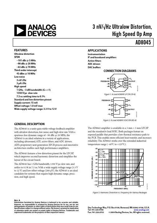
HARMONIC DISTORTION (dBc)
–20 G = +1
–30 VS = ±5V VOUT = 2V p-p
–40 RL = 1kΩ RS = 100Ω
–50
–60
–70
–80 –90 –100
HD3 LFCSP
HD2 LFCSP
–110
–120 0.1
1
10
100
FREQUENCY (MHz)
Fax: 781.326.8703 © 2004 Analog Devices, Inc. All rights reserved.
元器件交易网
AD8045
TABLE OF CONTENTS
Specifications with ±5 V Supply ..................................................... 3 Specifications with +5 V Supply ..................................................... 4
Rev. A
Information furnished by Analog Devices is believed to be accurate and reliable. However, no responsibility is assumed by Analog Devices for its use, nor for any infringements of patents or other rights of third parties that may result from its use. Specifications subject to change without notice. No license is granted by implication or otherwise under any patent or patent rights of Analog Devices. Trademarks and registered trademarks are the property of their respective owners.
EFD15中文资料(ferroxcube)中文数据手册「EasyDatasheet - 矽搜」
阂 x仙 (mm 4)
251
类型编号
CPH-EFD15-1S-8PD-Z
2008年9月1
5
核心套
锁模力对于A GRADE
3C90
3C94
3C95 3C96 3F3
3F35 3F4
3F45 2008年9月1
L 测量,20
AL (nH) 63 ±5% 100 ±8% 160 ±10% 950 ±25% 63 ±5% 100 ±8% 160 ±10% 950 ±25% 1140 ±25% 850 ±25% 63 ±5% 100 ±8% 160 ±10% 780 ±25% 630 ±25% 63 ±5% 100 ±8% 160 ±10% 400 ±25% 400 ±25%
13.75 3.75
Dimensionsin mm.
图3 EFD15/8/5线圈架; 8针.
绕组数据和区域产品 EFD15/8/5线圈架( PCB) ,具有 8管脚
单位数
SECTIONS
1
绕组
AREA (mm 2)
16.7
最低 绕组
WIDTH (mm)
9.15
平均 长研究
TURN (mm)
25.6
AREA
3.75 13.75
1.3 0 0.15
Dimensionsin mm.
图2 EFD15/8/5线圈架; 8针.
绕组数据和区域产品 EFD15/8/5线圈架具有 8管脚
单位数
SECTIONS
1
绕组
AREA (mm 2)
14.8
最低 绕组
WIDTH (mm)
8.85
Note 1.也可与后插入针.
平均 长研究
AD847ARZ中文资料

a
FEATURES Superior Performance
High Unity Gain BW: 50 MHz Low Supply Current: 5.3 mA High Slew Rate: 300 V/s Excellent Video Specifications
AD847 Driving Capacitive Loads
One Technology Way, P.O. Box 9106, Norwood, MA 02062-9106, U.S.A.
Tel: 617/329-4700
Fax: 617/326-8703
元器件交易网
QUIESCENT CURRENT – mA
5.5
5
4.5
4
0
5
10
15
20
SUPPLY VOLTAGE – ± Volts
Quiescent Current vs. Supply Voltage
REV. F
Information furnished by Analog Devices is believed to be accurate and reliable. However, no responsibility is assumed by Analog Devices for its use, nor for any infringements of patents or other rights of third parties which may result from its use. No license is granted by implication or otherwise under any patent or patent rights of Analog Devices.
ADDA的常用芯片简介
AD/DA的常用芯片简介如今出产AD/DA的首要厂家有ADI、TI、BB、PHILIP、MOTOROLA等,武汉力源公司具有多年从事电子商品的履历和雄厚的技才调气支撑,已获得排行国际前列的仿照IC出产厂家ADI、TI 公司署理权,运营全系列适用各种范畴/场合的AD/DA器材。
1.AD公司AD/DA器材AD公司出产的各种模数改换器(ADC)和数模改换器(DAC)(总称数据改换器)一贯坚持商场领导方位,包含高速、高精度数据改换器和如今盛行的微改换器体系(MicroConvertersTM)。
1)带信号调度、1mW功耗、双通道16位AD改换器:AD7705 AD7705是AD公司出品的适用于低频丈量仪器的AD改换器。
它能将从传感器接纳到的很弱的输入信号直接改换成串行数字信号输出,而无需外部外表拓宽器。
选用Sigma;-Delta;的ADC,完毕16位无误码的超卓功用,片内可编程拓宽器可设置输入信号增益。
经过片内操控寄存器调整内部数字滤波器的封闭时刻和更新速率,可设置数字滤波器的榜首个凹口。
在+3V电源和1MHz主时钟时,AD7705功耗仅是1mW。
AD7705是依据微操控器(MCU)、数字信号处理器(DSP)体系的志向电路,能够进一步节约本钱、减小体积、减小体系的凌乱性。
运用于微处理器(MCU)、数字信号处理(DSP)体系,手持式仪器,散布式数据搜团体系。
2)3V/5VCMOS信号调度AD改换器:AD7714AD7714是一个无缺的用于低频丈量运用场合的仿照前端,用于直接从传感器接纳小信号并输出串行数字量。
它运用Sigma;-Delta;改换技能完毕高达24位精度的代码而不会扔掉。
输入信号加至坐落仿照调制器前端的专用可编程增益拓宽器。
调制器的输出经片内数字滤波器进行处理。
数字滤波器的初度陷波经过片内操控寄存器来编程,此寄存器能够调度滤波的截止时刻和树立时刻。
AD7714有3个差分仿照输入(也可所以5个伪差分仿照输入)和一个差分基准输入。
AOZ1015AI中文资料
Page 1 of 15
元器件交易网
AOZ1015
Ordering Information
Part Number
AOZ1015AI
S nt RoH plia Com
Ambient Temperature Range
0.96V
+ –
Over Voltage Protection Comparator
AGND
PGND
Absolute Maximum Ratings
Exceeding the Absolute Maximum ratings may damage the device.
Recommend Operating Ratings
Rev. 1.2 September 2007
Page 2 of 15
元器件交易网
AOZ1015
Block Diagram
VIN
EN
UVLO & POR
5V LDO Regulator
Internal +5V
OTP
+
ISen Reference & Bias
Applications
● ● ● ● ● ● ●
Point of load DC/DC conversion PCIe graphics cards Set top boxes DVD drives and HDD LCD panels Cable modems Telecom/networking/datacom equipment
Parameter
Supply Voltage Input Under-Voltage Lockout Threshold Supply Current (Quiescent) Shutdown Supply Current Feedback Voltage Load Regulation Line Regulation
AD8015ARZ,AD8015ARZ-REEL7,AD8015AR, 规格书,Datasheet 资料
NOTES 1Stresses above those listed under “Absolute Maximum Ratings” may cause permanent damage to the device. This is a stress rating only and functional operation of the device at these or any other conditions above those indicated in the operational section of this specification is not implied. Exposure to absolute maximum rating conditions for extended periods may affect device reliability. 2Specification is for device in free air: 8-pin SOIC package: θJA = 155°C/W.
dB
40
dB
OUTPUT
Differential Offset
6
20
mV
Output Common-Mode Voltage
From Positive Supply
–1.5
–1.3
–1.1
V
Voltage Swing (Differential) Output Impedance
Positive Input Current, RL = ∞ Positive Input Current, RL = 50 Ω
Figure 2. Noise vs. Frequency (SO-8 Package with Added Capacitance)
AD8321ARZ中文资料
Interactive CATV Set-Top Boxes
CATV Plant Test Equipment
General Purpose IF Variable Gain Block
VCC
Gain Programmable CATV Line Driver AD8321
FUNCTIONAL 43; INV VIN– ATTENUATOR CORE
PWR AMP VOUT REVERSE AMP
DATA LATCH DATA SHIFT REGISTER POWERDOWN/ SWITCH INTER PD
DATA SHIFT REGISTER
All Gain Codes f = 65 MHz f = 65 MHz All Gain Codes, Full Temperature Range Max Gain, f = 10 MHz Min Gain, f = 10 MHz Output Noise Temperature Sensitivity 0 £ TA £ +70∞C, Min Gain Power-Down Spectral Density 1 dB Compression Point Max Gain, f = 10 MHz Output Impedance Power-Up and Power-Down f = 42 MHz, POUT = 11 dBm, VCC = +9 V f = 65 MHz, POUT = 11 dBm, VCC = +9 V –40∞C £ TA £ +85∞C f = 10 MHz, All Gain Codes 0 £ TA £ +70∞C Min to Max Gain, VIN = 0 V Max Gain, VIN = 0.15 V Step Power Down, 65 MHz, Min Gain VIN = 0.137 V p-p Max Gain, VIN = 0 Max Gain, VIN = 0 Max Gain, VIN = 0 Max Gain, VIN = 0 Power-Up, VCC = +9 V Power-Down, VCC = +9 V