XL1530原厂规格书(2014版)
邦纳 安全光幕

EZ-SCREEN TM2一种具备30mm 分辨率和15m 保护距离的低成本保护系统在危险低的区域保护采用EZ-SCREEN ®2级安全光幕,这是一种比较经济的解决方案。
危险低的环境是指意外事故的发生只会引起一些小的伤害,像肿伤、撞伤、跌伤、夹伤(但没有骨折)、割伤及擦伤。
具备30mm 的分辨率,可以检测小的物体,诸如手掌或脚踝,工作距离可达到15m ,具有广泛的应用。
符合二级的设计标准EZ-SCREEN ®2级满足抗震动、冲击试验、光性能及使用安全标准(IEC61496-1/-2与EN954-1)的二级应用的所有需求,具有连续的自诊断功能和外围设备控制的故障检测功能,是专为低危险程度保护而设计应用的,不建议用在手工危险操作的保护应用。
小巧、简单的两件式系统EZ-SCREEN ®2级是一种小巧的两件式系统,不需要单独的控制器,仅需包含了各自电源和光学同步功能的发射器和接收器即可,除去了DIP 开关功能选择或程序设定的调试功能,只要安装后就可使用。
可选手动或自动复位输出,响应速度快采用EZ-SCREEN ®2级,当遮挡光束消除时,需要自动复位输出可选择带T 的接收器型号,需要手动复位输出(如典型的安全门应用)可选择带L 的接收器型号。
优秀的2级设计具有极快的响应速度,11ms 到25ms 就可使设备迅速停机。
简单明了的诊断EZ-SCREEN ®2级具有非常明显的LED 状态指示灯:• 电源指示• 故障指示(LED 闪烁)• 顶部和底部光束接受指示• 光束或输出状态:遮挡或对准Trip 接收器Latch 接收器发射器3EZ-SCREEN 系统30mm 分辨率、8针M12(Euro 型)针式连接器接线的EZ-SCREEN 二级安全光幕各型号如下:单件或成对采购都可EZ-SCREEN 二级电缆4EZ-SCREEN TM 2级系统套装型号解析安全继电器模块EZ-SCREEN ®2级系统,可以单独购买,成对购买或套装购买,套装型号解析请看以下图示。
铝合金制品规格书

铝合金制品规格书1. 引言铝合金制品规格书是指对铝合金制品的各项技术要求、性能指标、检验方法等进行详细描述的文件。
本规格书旨在确保铝合金制品的质量,满足客户需求,并提供制造和检验的依据。
2. 适用范围本规格书适用于所有铝合金制品,包括但不限于铝合金型材、铝合金板材、铝合金管材等。
3. 规范引用在编写本规格书时,参考了以下标准和规范: - GB/T 3190-2010 铝及铝合金化学成分 - GB/T 3880-2012 铝及铝合金板材 - GB/T 6892-2006 铝及铝合金挤压型材- GB/T 5237.1-2008 铝型材表面处理4. 术语和定义4.1 铝合金制品指以铝为主要成分,添加其他元素而形成的具有特定性能和用途的产品。
4.2 型号根据不同的标准或客户要求,对不同种类的铝合金制品进行分类和命名的编号。
4.3 规格指铝合金制品的尺寸、形状、工艺要求等详细描述。
4.4 抗拉强度指铝合金制品在拉伸试验中最大承受的力,单位为兆帕(MPa)。
5. 技术要求5.1 化学成分铝合金制品的化学成分应符合GB/T 3190-2010标准中规定的要求。
5.2 物理性能铝合金制品的物理性能应符合以下要求: - 密度:不大于2.8 g/cm³; - 热膨胀系数:在20℃至100℃范围内,不大于24×10^-6/℃; - 硬度:根据型号和用途确定; - 弯曲强度:根据型号和用途确定。
5.3 表面处理铝型材表面处理应符合GB/T 5237.1-2008标准中规定的要求,常见表面处理方法包括氧化、喷砂、阳极氧化等。
5.4 尺寸和公差铝合金制品的尺寸和公差应符合相关标准或客户要求。
具体尺寸和公差范围可参考GB/T 3880-2012和GB/T 6892-2006标准。
5.5 表面质量铝合金制品的表面应平整、光洁,不得有明显的划痕、气泡、裂纹等缺陷。
具体要求可根据型号和用途确定。
5.6 抗拉强度铝合金制品的抗拉强度应符合相关标准或客户要求。
XL原厂资料 上海芯龙型号大全

⧄⺇ㅖ䁚㋋䐒㒘⮈䊕⢅㾟㠍㬨㬱⧂㿉㤔㑠䔏⫔⭥㋋⮈䊕㾟㠍゙᷍爪㉙⫔ⱁ㭞⭥⮈䓴㪉⡙䐱Ⱍ。䇤⭞᷍ 㾟㒛⤪䇤䄖ㆈ㻩㆙⭥䐧䋍⹅䄶᷍㳂⹊㭅㧌⮈䁚⪴5V⭞90V᷍㭅⨗⮈㒘㚽㑇⪴0⭞A᷍㋋㠖㔫⤜㵍᷍ⴃ䓑㶃㾯⤜㵍᷍ ⷀ㾈㔫᷍ⷀ⹇㔫㗽Ⱙ᷍ⷀ㾵ゼ⡩⭥㦌㻖㑱ㅖ䁚㋋䐒㒘⮈䊕⢅㾟㠍ᷜ
斤䁚斤㒘ㅖ䁚㋋䐒㒘⮈䊕⢅㡘
㡔䄖㸥鼻
䄵㬱⧂㋮黃㸋⭝㼓 㛞㈼䇻屮㾥㈛䎚㑇 㳂⹊㔭㩌⡄⥛㠘 ⧷㿙㸩ㅂ㾎⮘ⳃ䍚
⤠䐋㬗⥛㦉䐅㭊
芯龙半导体 华南地区一级代理 森利威尔电子有限公司 联系人:曾先生 手机;13534002546 QQ:2355368875 欢迎各位来电咨询、可免费提供样品测试!
㩰乙㾟㒛⟌⭝㳆ゝ㭖⳾䇱㻿⹌㯟
⹌㯟ビㆊ
㩰乙㾟㒛⟌⭝㳆ゝ㭖⳾䇱㻿⹌㯟㬨䄜コ䓉䄖⪴㬣⮈䊕㏎㏁㚄㛃ゐ⧪⮈㔘㋋ⳃ⭥㪉ェ⹌㯟ᷜ㾟 㒛⭥屮㾥䁱ⳃ巛㏎㵦ⰴ䇪䄜㞛㎕䓵䄖ㆈⰆッ⟌⭝㳆㪉ェ⹌㯟⭥䓫㪏䓉コ䔊⧪ᷜ㾟㒛ㅌ䄖ㆈ㻩㆙⭥㪉 ェゝ㭖䈌䁨㲌⭹㤙⭥⡟㵢䇦㬧⥛䄖㑕㼁ㆂ己᷍ⴟ㹒㦌㤓㬱⧂᷍㸋㋮黃㳂⹊㌍㯺᱃ⷀ㾈᱃ⷀ㾵ゼ⡩⭥㦌 㻖㑱⮈䊕㏎Ⳟ➙巛ⴟ㹒᱄ 㾟㒛⟌⭝㳆䊻ⷀ䁚᱃ⷀ㾈㔫᱃⫔⹇㔫⭥⮈䊕㏎ゐ⧪⮈㔘㒍䈓䇖䇱ⱁ㼏屮㾥䓉㏜ゝ㭖ᷜ⥛㠘䑘䄋 䇇䇤㪇ゑ㬷⧷㬞⢄㾐㬞⮈䓴⥛㠘᱃㼜Ⳳ㏁コ䇤⮈㡘᱃㡜⧖⮈䓴᱃⹅䄖㋹䐧巛ェ㰄〛᱃⟌⭝㳆䍶㘘᱃㾣 㚽䊕㏎᱃ⱁ㗞㳆䅕㬴㠖⭩㒍䈓᱄㾟㒛⟌⭝㳆䇖䇱䓵䑘䐋㬗⥛㦉⭥ⷀ䁚䐧⧭᱃⪕㾣⭥㪉ェ㏎㛏᱃䓉䄖 ⭥⹇㔫㾟㠍ⴃ䓑⹅䄶ᷜ䊻ⷀ⮈䁚᱃⫔⹇㔫⭆㠍㋋⮈䊕ゐ⧪⮈㔘㒍䈓巛⫔⹇㔫/('䍶㘘㒍䈓⪇䇻䄖ㆈ 㒍㻩⭹㸜᱄ 㾟㒛⟌⭝㳆㬝䐶ヂ⧷䄵᱑䓉䄖᱃䓉䓃᱃㹒㬖᱃⪕㾣᱃ⷀ㾈᱃⹖㵉᱒㸋㈎䇋㏎㛏᷍⢝⧱䈌㤟⭡㩭⭥ ᱑䓫䊕⹓㼎᱃己䔘⹓䇏᱒⭥䊎䋓᷍㸋㋮黃㳂⹊ⷀ㾵ゼ⡩᱃㉀䇱䓵䑘䐋㬗⥛㦉⭥⟌⭝㳆㈌㠘㾟㠍᱃ㆃ㉗ Ⳟ➙ゑ䇦䐫ⴟ㹒᱄㾟㒛⟌⭝㳆䐣㑇⧪㸋㬡ㆈ䄜㒘⭥⮈䊕㏎㏁㚄㛃ゐ⧪⮈㔘㪉ェ⹌㯟᱄
MBR1530CT;MBR1535CT;MBR1540CT;MBR1545CT;MBR1550CT;中文规格书,Datasheet资料
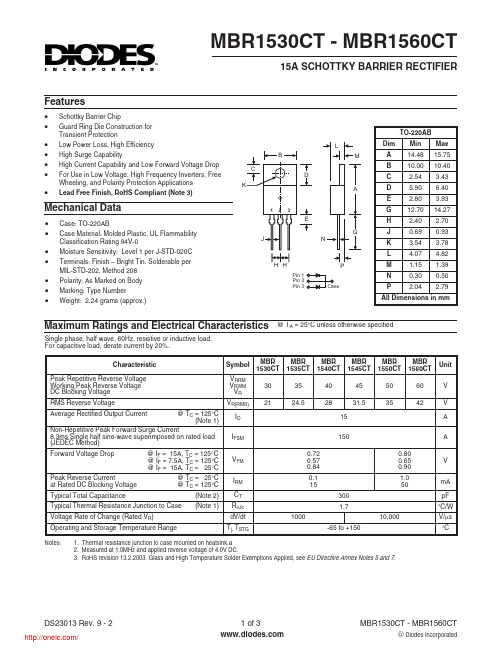
MBR1530CT - MBR1560CT15A SCHOTTKY BARRIER RECTIFIERFeaturesPin 1Pin 3Pin 2Maximum Ratings and Electrical Characteristics@ T A = 25°C unless otherwise specified·Schottky Barrier Chip·Guard Ring Die Construction for Transient Protection·Low Power Loss, High Efficiency ·High Surge Capability·High Current Capability and Low Forward Voltage Drop ·For Use in Low Voltage, High Frequency Inverters, Free Wheeling, and Polarity Protection Applications ·Lead Free Finish, RoHS Compliant (Note 3)Mechanical Data·Case: TO-220AB·Case Material: Molded Plastic. UL Flammability Classification Rating 94V-0·Moisture Sensitivity: Level 1 per J-STD-020C ·Terminals: Finish – Bright Tin. Solderable per MIL-STD-202, Method 208·Polarity: As Marked on Body ·Marking: Type Number ·Weight: 2.24 grams (approx.)Single phase, half wave, 60Hz, resistive or inductive load.For capacitive load, derate current by 20%.Notes:1. Thermal resistance junction to case mounted on heatsink.a2. Measured at 1.0MHz and applied reverse voltage of 4.0V DC.3.RoHS revision 13.2.2003. Glass and High Temperature Solder Exemptions Applied, see EU Directive Annex Notes 5 and 7.0.11.010500.20.40.60.81.0I ,I N S T A N T A N E O U S F W D C U R R E N T (A )F V ,INSTANTANEOUS FORWARD VOLTAGE (V)Fig.2Typical Forward CharacteristicsF050100150200250300110100I ,P E A K F O R W A R D S U R G E C U R R E N T (A )F S M NUMBER OFCYCLES AT 60HzFig.3Max Non-Repetitive Surge Current100100040000.11.010100C ,C A P A C I T A N C E (p F )T V ,REVERSE VOLTAGE (V)Fig.4Typical Total Capacitance (per element)R 0.0010.010.11.01020406080100120140I ,I N S T A N T A N E O U S R E V E R S E C U R R E N T (m A )R PERCENT OF RATED PEAK REVERSE VOLTAGE (%)Fig.5Typical Reverse Characteristics04850100150I ,A V E R A G E F O R W A R D C U R R E N T(A )(A V )T ,CASE TEMPERATURE (C)Fig.1Forward Current Derating CurveC °121620Ordering Information(Note 4)Notes: 4. For Packaging Details, go to our website at /datasheets/ap02007.pdf.分销商库存信息:DIODESMBR1530CT MBR1535CT MBR1540CT MBR1545CT MBR1550CT MBR1560CT。
MAX15301数据手册中文版

MAX15301是一个全功能,高效,数字化的点负载(POL)操纵器与先进的电源治理和遥测功能与PID 为基础的数字电源稳压器,MAX15301采纳Maxim拥有专利的Intune的™自动补偿,状态空间操纵算法。
Intune 的操纵律是有效的小信号和大信号响应,占占空比饱和度的阻碍。
这排除需要用户以确信和设置的阈值从线性转换到非线性模式。
这些能力在快速环路的瞬态响应,并减少输出电容器的数量相较,竞争的模拟和数字操纵器。
MAX15301包括多种功能,以优化效率。
内部开关BabyBuck的稳压器可产生栅极驱动器和内部偏置电源,低功耗的操纵器。
一种先进的,高效率的MOSFET的栅极驱动器,具有自适应非重叠按时,而持续调整的高侧和低侧的按时和驱动电压的全范围内的电压,电流和温度,以尽可能减少开关损耗。
MAX15301设计最终客户的设计环境的初衷。
上的PMBus™兼容的串行总线接口进行通信的监控器监控和故障治理。
全套的电源治理功能,无需复杂和昂贵的测序和监控IC。
大体的DC-DC转换操作,可设置通过引脚搭接,并非需要用户配置固件。
这使得电源子系统的快速进展前完成板级系统的工程。
Maxim提供支持的硬件和软件配置MAX15301 ,MAX15301可在32引线,5mm×5mm TQFN封装,工作在-40°C至+85°C的温度范围内。
特点:的自动补偿功能能够确保稳固,同时优化瞬态性能2.在快速瞬态响应减少输出电容的非线性补偿结果3.差分远端电压传感许诺±1%V OUT精度在整个温度范围内(-40°C至+85°C)接口用于配置,操纵和监测5.支持电压定位6.提高效率(自适应非重叠时序驱动器)至14V的宽输入电压范围8.高效片上BabyBuck稳压器的自偏置9.输出电压范围从到10.进入预偏置输出启动11.可配置的软启动和软停止时刻12.固定工作频率同步(300kHz至1MHz)13.灵活的排序和故障治理14.引脚手动跳线配置(输出电压,从机地址,开关频率,电流限制)15.能够快速原型图表典型工作电路引脚名字功能1SYNC外部开关频率同步输入端。
XL6001原厂规格书(2014版)
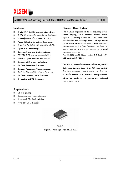
400KHz 32V 2A Switching Current Boost LED Constant Current Driver XL6001Featuresn Wide 3.6V to 24V Input Voltage Rang n0.22V Constant Current Sense Voltage n Directly drive 3~8 Series 1W LEDn Fixed 400KHz Switching Frequency n Max. 2A Switching Current Capability n Up to 92% efficiencyn Excellent line and load regulationn EN PIN TTL shutdown capabilityn Internal Optimize Power MOSFETn Built in LED Open Protectionn Built in Soft-Start Functionn Built in Frequency Compensationn Built in Thermal Shutdown Function n Built in Current Limit Functionn Available in SOP8 package Applicationsn LED Lightingn Boost constant current drivern Monitor LED Backlightingn7’ to 15’ LCD Panels General DescriptionThe XL6001 regulator is fixed frequency PWM Boost (step-up) LED constant current driver, capable of driving Series 1W LED units with excellent line and load regulation. The regulator is simple to use because it includes internal frequency compensation and a fixed-frequency oscillator so that it requires a minimum number of external components to work.The XL6001 could directly drive 5~8 Series 1W LED units at VIN>12V .The PWM control circuit is able to adjust the duty ratio linearly from 0 to 90%. An enable function, an over current protection function is built inside. An internal compensation block is built in to minimize external component count.Figure1. Package Type of XL6001400KHz 32V 2A Switching Current Boost LED Constant Current DriverXL6001Pin ConfigurationsSWEN FB VIN NCSW GNDGNDFigure2. Pin Configuration of XL6001 (Top View)Table 1 Pin DescriptionPin NumberPin Name Description1 ENEnable Pin. Drive EN pin low to turn off the device, drive ithigh to turn it on. Floating is default high.2 VINSupply V oltage Input Pin. XL6001 operates from a 3.6V to 24V DC voltage. Bypass Vin to GND with a suitably large capacitor to eliminate noise on the input.3 FB Feedback Pin (FB). The feedback threshold voltage is 0.22V .4 NC No Connected.5,6 SWPower Switch Output Pin (SW). Output is the switch node thatsupplies power to the output.7,8 GND Ground Pin.400KHz 32V 2A Switching Current Boost LED Constant Current Driver XL6001 Function BlockFigure3. Function Block Diagram of XL6001Typical Application CircuitFigure4. XL6001 Typical Application Circuit400KHz 32V 2A Switching Current Boost LED Constant Current Driver XL6001Ordering InformationPart Number Marking ID Lead Free Lead Free Packing Type XL6001E1 XL6001E1 Tube PackageTemperature RangeXL6001TRE1XL6001E1Tape & ReelXLSEMI Pb-free products, as designated with “E1” suffix in the par number, are RoHS compliant.Absolute Maximum Ratings (Note1)ParameterSymbol Value Unit Input VoltageVin -0.3 to 26 V Feedback Pin Voltage V FB -0.3 to Vin V EN Pin VoltageV EN -0.3 to Vin V Output Switch Pin Voltage V Output -0.3 to 32 V Power DissipationP D Internally limitedmW Thermal Resistance (SOP8)(Junction to Ambient, No Heatsink, Free Air) R JA 100 ºC/W Operating Junction Temperature T J -40 to 125 ºC Storage TemperatureT STG -65 to 150 ºC Lead Temperature (Soldering, 10 sec) T LEAD 260 ºC ESD (HBM)>2000VNote1: Stresses greater than those listed under Maximum Ratings may cause permanent damage to the device. This is a stress rating only and functional operation of the device at these or any other conditions above those indicated in the operation is not implied. Exposure to absolute maximum rating conditions for extended periods may affect reliability.400KHz 32V 2A Switching Current Boost LED Constant Current Driver XL6001 XL6001 Electrical CharacteristicsT a = 25℃;unless otherwise specified.Symbol Parameter Test Condition Min. Typ. Max. Unit System parameters test circuit figure4VFB FeedbackV oltageVin = 5V to 12V, V out=24VIload=100mA209 220 231 mVEfficiency ŋVin=12V ,V out= 6*1W LEDIout=0.3A- 92 - %Electrical Characteristics (DC Parameters)Vin = 12V, GND=0V, Vin & GND parallel connect a 47uf/25V capacitor; Iout=50mA, T a = 25℃; the others floating unless otherwise specified.Parameters Symbol Test Condition Min. Typ. Max. Unit Input operation voltage Vin 3.6 24 V Shutdown Supply Current I STBY V EN=0V 70 100 uAQuiescent Supply Current I q V EN =2V,V FB =Vin2.5 5 mAOscillator Frequency Fosc 320 400 480 Khz Switch Current Limit I L V FB =0 2 AOutput Power NMOS Rdson Vin=12V,I SW=2A110 120 mohmEN Pin Threshold V EN High (Regulator ON)Low (Regulator OFF)1.40.8VI H V EN =2V (ON) 3 10 uA EN Pin Input LeakageCurrent ILV EN =0V (OFF) 3 10 uA Max. Duty Cycle D MAX V FB=0V 90 %400KHz 32V 2A Switching Current Boost LED Constant Current Driver XL6001Schottky Diode Selection TableCurrent SurfaceMountThrough Hole VR (The same as system maximum input voltage)20V 30V 40V 50V60V1A √1N5817 1N5818 1N5819√ 1N5820 1N5821 1N5822√ MBR320 MBR330 MBR340 MBR350 MBR360 √ SK32 SK33 SK34SK35SK36 √ 30WQ03 30WQ04 30WQ05 √ 31DQ03 31DQ04 31DQ05 3A√SR302SR303SR304SR305SR306Typical System Application for VIN=5V to driver 2~6 x 1W series LED unitsFigure5. XL6001 System Parameters Test Circuit (2~6 x 1W LED)400KHz 32V 2A Switching Current Boost LED Constant Current Driver XL6001 Typical System Application for VIN=12V to driver 4~8 x 1W series LED unitsFigure6. XL6001 System Parameters Test Circuit (4~8 x 1W LED)Typical System Application for VIN=12V to driver 4~8 x 1W series LED units With PWM DimmingFigure7. XL6001 System Parameters Test Circuit (4~8 x 1W LED with PWM Dimming)400KHz 32V 2A Switching Current Boost LED Constant Current Driver XL6001 Typical System Application for SEPIC Buck-Boost LED DriverFigure8. XL6001 System Parameters Test Circuit (Buck-Boost LED Driver)400KHz 32V 2A Switching Current Boost LED Constant Current Driver XL6001 Package InformationSOP8 Package Mechanical Dimensions。
电动订书机产品规格书
电动订书机产品规格书
1、适用范围
本规格书适用于DXC公司生产的电动订书机。
2、定义
2.1电动订书机:当纸触发入纸口感应开关时,通过线线路和机械联动,在
要求位置打钉的装置。
2.2正常电压:对额定电压120VAC/60Hz为120VAC/60Hz;对额定电压
220~240VAC/50Hz为230 VAC/50Hz。
2.3低电压:对额定电压120VAC/60Hz为105VAC/60Hz;对额定电压
220~240VAC/50Hz为198 VAC/50Hz。
2.4高电压:对额定电压120VAC/60Hz为130VAC/60Hz;对额定电压
220~240VAC/50Hz为264 VAC/50Hz。
3、产品规格
3.1特性/参数
3.2外观与颜色
--外观、颜色不可有明显的缺点,如脱色、凹陷、裂痕及脏污;
--印有指示应正确、及印于规定位置;
--外壳应光滑,不能有利边,且段差小于0.3mm;
--外观型状与结构图相符,如不能以结构图作出评定标准,则与“可接收”样板相符;
--详细颜色参考《YRS309BOM》。
3.3主要部件材质
3.4标识。
易通 HT1530 贴片机用户手册说明书

目录1.用户注意事项 (2)安全提示 (2)注意事项 (2)2.机器安装与调校 (2)2.1工作环境及条件 (2)2.2机器安装 (2)2.3机器调校 (3)2.4装箱清单 (3)3.机器说明书 (3)3.1概述 (3)3.2主要技术参数 (4)3.3机器工作流程 (4)3.4机器操作说明 (5)3.4.1通电前检查 (5)3.4.2确定贴装方式及数量 (6)3.4.3调节头部及飞达间距 (6)3.4.4调节吸嘴及飞达间距 (11)3.4.5贴装程序 (13)3.4.6做MARK点 (19)3.5常见问题与处理 (22)4.电气控制电路图 (24)4.1 电箱布局图 (24)4.2电路控制图 (25)5、维护与保养 (32)5.1吸嘴保养 (32)5.2飞达工作台保养 (34)5.3导轨和丝杆保养 (34)5.4飞达维修与保养 (35)5.5真空泵维护与保养 (37)6.机器保修信息 (39)6.1保修卡 (39)6.2维修记录卡 (41)7.售后服务信息 (42)1.用户注意事项感谢您使用深圳市易通自动化机器有限公司生产的H T1530系列L E D贴片机!安全提示:● 本机器只能由专业维护及维修人员或培训合格的人员进行操作● 通电之前,应确认外接输入电源与该机器的额定电压及电流相符● 本机器内含运动装置及机械传动,操作时应注意人身安全注意事项:●操作本机器前请仔细阅读本用户手册● 请不要把本机器安装在电磁干扰源附近● 请使用规定的电压、电流、功率(详见机器安装与调校)● 机器不使用时,请关闭电源、气源● 保养、维修之前,请关闭机器电源● 请按本手册要求定期对机器进行保养● 勿改变本机器电控箱内的软体及硬体设置● 请妥善保管本手册,以便维护保养及维修时查阅2.机器安装与调校2.1工作环境及条件1.本设备应放置在平坦坚固地面;2.工作环境温度应在22~28℃之间;3.工作环境湿度应在45~75RH%之间;4. 机器附近不能有强磁场;5. 使用具有三相AC380V(50-60HZ)稳定电压的电源(保证接地良好);6. 使用气源0.5~0.6MPa(气源为大气压霜点:-17℃以下,微粒粉:粒径5μm以下,最高油分浓度:5㎎/m以下)。
- 1、下载文档前请自行甄别文档内容的完整性,平台不提供额外的编辑、内容补充、找答案等附加服务。
- 2、"仅部分预览"的文档,不可在线预览部分如存在完整性等问题,可反馈申请退款(可完整预览的文档不适用该条件!)。
- 3、如文档侵犯您的权益,请联系客服反馈,我们会尽快为您处理(人工客服工作时间:9:00-18:30)。
XL1530
FB EN NC VIN
1 2 XL1530 3 4
8 7 6 5
GND GND SW SW
Figure2. Pin Configuration of XL1530 (Top View) Table 1 Pin Description Pin Number 3 4 5,6 7,8 Pin Name NC VIN SW GND Description No Connected. Supply Voltage Input Pin. XL1530 operates from a 3.6V to 18V DC voltage. Bypass Vin to GND with a suitably large capacitor to eliminate noise on the input. Power Switch Output Pin (SW). Output is the switch node that supplies power to the output. Ground Pin. Care must be taken in layout. This pin should be placed outside of the Schottky Diode to output capacitor ground path to prevent switching current spikes from inducing voltage noise into XL1530. Feedback Pin (FB). Through an external resistor divider network, Feedback senses the output voltage and regulates it. The feedback threshold voltage is 0.8V. Enable Pin. Drive EN pin low to turn off the device, drive it high to turn it on. Floating is default high.
ŋ
Electrical Characteristics (DC Parameters)
Vin = 12V, GND=0V, Vin & GND parallel connect a 220uf/50V capacitor; Iout=500mA, Ta = 25℃; the others floating unless otherwise specified. Parameters Input operation voltage Shutdown Supply Current Quiescent Supply Current Oscillator Frequency Switch Current Limit EN Pin Threshold EN Pin Input Leakage Current Max. Duty Cycle Symbol Vin ISTBY Iq Fosc IL VEN IH IL DMAX VFB =0 High (Regulator ON) Low (Regulator OFF) VEN =2V (ON) VEN =0V (OFF) VFB=0V VEN=0V VEN =2V, VFB =Vin 323 Test Condition Min. 3.6 60 3 380 4.7 1.4 0.8 1 1 100 15 15 Typ. Max. 18 200 5 437 Unit V uA mA Khz A V uA uA %
XL1530
Package
Temperature Range
XLSEMI Pb-free products, as designated with “E1” suffix in the par number, are RoHS compliant.
Absolute Maximum Ratings(Note1)
Applications
LCD Monitor and LCD TV Digital Photo Frame Set-up Box ADSL Modem Telecom / Networking Equipment
Figure1. Package Type of XL1530
1
3A 380KHz 18V Buck DC to DC Converter Pin Configurations
3A 380KHz 18V Buck DC to DC Converter Features
ቤተ መጻሕፍቲ ባይዱ
XL1530 General Description
The XL1530 is a 380KHz fixed frequency PWM buck (step-down) DC/DC converter, capable of driving a 3A load with high efficiency, low ripple and excellent line and load regulation. Requiring a minimum number of external components, the regulator is simple to use and include internal frequency compensation and a fixed-frequency oscillator. The PWM control circuit is able to adjust the duty ratio linearly from 0 to 100%. An enable function, an over current protection function is built inside. When short protection function happens, the operation frequency will be reduced from 380KHz to 80KHz. An internal compensation block is built in to minimize external component count.
XL1530
System parameters test circuit figure4 VFB Efficiency Feedback Voltage Vin = 7V to 18V, Vout=5V Iload=0.2A to 3A Vin=12V ,Vout=5V Iout=3A 0.776 0.8 88 0.824 V %
Note1: Stresses greater than those listed under Maximum Ratings may cause permanent damage to the device. This is a stress rating only and functional operation of the device at these or any other conditions above those indicated in the operation is not implied. Exposure to absolute maximum rating conditions for extended periods may affect reliability.
Parameter Input Voltage Feedback Pin Voltage EN Pin Voltage Output Switch Pin Voltage Power Dissipation Thermal Resistance (SOP8) (Junction to Ambient, No Heatsink, Free Air) Operating Junction Temperature Storage Temperature Lead Temperature (Soldering, 10 sec) ESD (HBM) Symbol Vin VFB VEN VOutput PD RJA TJ TSTG TLEAD Value -0.3 to 20 -0.3 to Vin -0.3 to Vin -0.3 to Vin Internally limited 100 -40 to 125 -65 to 150 260 2000 Unit V V V V mW ºC/W ºC ºC ºC V
Rev 1.0 5
Datasheet 3A 380KHz 18V Buck DC to DC Converter XL1530
Test Circuit and Layout guidelines
Figure5. Standard Test Circuits and Layout Guides Select R1 to be approximately 2K, use a 1% resistor for best stability. C1 and CFF are optional; in order to increase stability and reduce the input power line noise, CIN and C1 must be placed near to VIN and GND; For output voltages greater than approximately 10V, an additional capacitor CFF is required. The compensation capacitor is typically between 100 pf and 33 nf, and is wired in parallel with the output voltage setting resistor, R2. It provides additional stability for high output voltage, low input-output voltages, and/or very low ESR output capacitors, such as solid tantalum capacitors. CFF=1/(31*1000*R2); This capacitor type can be ceramic, plastic, silver mica, etc. (Because of the unstable characteristics of ceramic capacitors made with Z5U material, they are not recommended.)