
带预热和功率MOS管的节能灯芯片UBA2211中文规格书
UBA2211驱动CFL的半桥功率集成电路产品数据手册1.概述UBA2211是一种高压单片集成电路,采用半桥结构,用于驱动的紧凑型荧光灯(CFL)。
该系列产品提供了简单一体化的照明控制方案,适用于各种市电输入和功率范围的灯管。
专利技术和集成保护类型:·预热阶段t)和预热电流。
在启动阶-- 预热应用:可调节的预热电流控制模式,调节预热时间(ph段触发该模式-- 非预热应用:点火后,专用的辉光时间控制,最小化电极点火损害。
·电流饱和保护(SCP):在点火阶段,提供专门饱和保护。
这确保了灯电感运行在饱和电流以下,且不超过集成半桥功率管的额定电流。
·RMS电流控制f保证RMS电流为恒值。
正常工作下,将启芯片内部计算RMS电流,通过改变频率OSC动专门的RMS电流控制,保证恒定的灯电流和IC损耗,正常半桥灯管电流可以通过检测电R)来设定。
阻(SENSE·过热保护和电容模式保护在非标准条件下,过热和电容模式保护会对电路进行检测,确保系统正常关闭和在灯管达到使用寿命时,处于安全状态。
2.特性和优点2.1系统集成度·集成半桥功率晶体管UBA2211A:市电220V,导通阻抗13.5Ω,最大点火电流0.9AUBA2211B:市电220V,导通阻抗9Ω,最大点火电流1.35AUBA2211C:市电220V,导通阻抗6.6Ω,最大点火电流1.85A·集成自举二极管·集成高压供电电源2.2灯管寿命·电流控制预热,预热时间和电流可调·最小辉光时间支持冷起动·灯功率不受电源电压变化影响·点火期间电感饱和保护2.3安全性·过热保护·电容模式保护·过功率控制·灯管寿命终止时,系统自动关闭2.4 应用简单·可调工作频率,方便与各种灯管匹配·该系列各种型号包含相同的控制器功能,保证使用于各种功率范围的CFL。
3.应用·应用于室内和室外25W以下的紧凑型荧光灯4、订购信息表1:订购信息型号 封装名称 描述 版本UBA2211AP/N1 DIP8 塑料双列直插封装;8脚(300mil)SOT97-1UBA2211BP/N1UBA2211CP/N1UBA2211AT/N1 SO14 塑料小形封装;14脚;身宽3.9 mm SOT108-1UBA2211BT/N1UBA2211CT/N15.方框图在DIP8封装中,没有将二极管集成在内,需要在外部进行连接。
6.1管脚图2:DIP8管脚结构 图3: SO14(管脚tbd)的管脚结构6.2管脚描述 表2:管脚描述 符号 管脚 描述UBA2211XP UBA2211XT SW 1 8扫频时间/VCO 输入 SGND 2 1,2,9,10,13信号地FS 3 11 上桥浮动电源输出 SENSE 4 12 预热和RMS 控制电压检测 OUT 5 14 半桥输出 HV 6 3 高压电源V DD 7 6 内部低压电源输出 RC 8 7 内部振荡输入 DVDT n.p. 5 DVDT 电源输入 PGNDn.p.4DVDT 电源地7.功能描述7.1工作电源UBA2211系列通过启动电流和DD V 电源进行供电。
在管脚HV 电压上升时,DD V 电容(VDD C )通过一个内部的结型场效应管电流源充电。
直到管脚DD V 上的电压上升到DD V =)(start DD V ,启动电流源被禁用。
此时,半桥开始工作,DD V 电源改由充电泵供电。
DD V 流过的电流值等于HV DVDT V C f ××,f 为瞬时频率。
充电泵由外部半桥电容(DVDT C )、两个内置(只对于SO14封装)二极管和一个内置的齐纳二极管组成。
对于DIP8封装,这些二极管需要外接。
齐纳二极管保证DD V 电压不会超过最大DD V 额定值。
DVDT 电源含有自身的接地管脚(PGND),可以防止由外部小信号低(SGND)上产生的峰值电流影响。
启动电流源在管脚DD V 电压小于()stop DD V 时会再次工作。
当DD V 引脚上电源电压增加,IC进入启动阶段。
在启动阶段,上桥功率晶体管关断,下桥功率晶体管导通。
内部电路复位,引脚FS上的自举电容和低压电源引脚DD V 上的电容被充电。
引脚RC和SW对地短接。
当DD V 脚上电压大于)(start DD V ,系统退出启动阶段进入预热阶段。
如果DD V <)(stop DD V ,系统将回到启动状态。
注意:如果过温保护(OTP)被激活,只要该状态一直存在,IC将会维持在启动状态。
DD V 电压将会在)(stop DD V 和)(start DD V 之间缓慢振荡。
7.3复位上桥驱动电路中集成了DC复位功能。
当引脚FS上的电压低于上桥自锁电压时,上桥晶体管关断。
7.4振荡控制振荡频率基于555定时器功能实现。
利用外部电阻器osc R ,SENSE R 和电容器osc C ,实现一个自振荡电路,osc R 和osc C 决定振荡频率。
为了实现精确的50%占空比,在内部使用了一个分频电路。
该分频电路能将半桥频率设置为振荡器频率的一半。
管脚SW的输入产生信号SW V ,它决定了除预热阶段以外的所有阶段的频率,()ph SW V 是内部产生的信号,决定预热阶段的频率。
半桥输出电压在管脚RC信号的下降沿处改变。
半桥正常工作频率如式1所示:()1OSC nom OSC OSC OSCf k R C =×× (1)最大频率为2.5OSC f ×,通过SW V 来设置。
图4中给出了振荡器信号、内部LS 和HS 驱动信号、以及输出信号的对应时序波形。
图4:振荡器,HSPT/LSPT 驱动和输出信号7.5预热阶段7.2节中提到,当管脚电压(start)DD DD V V >且未触发OTP 时,IC 进入预热阶段。
管脚SW 上的电容(SW C )由SW I 充电,内部的运算放大器(OTA)被激活状态,半桥电路开始振荡。
通过外部电阻SENSE R 来检测预热电流。
OTA 通过输出电压(ph)SW V 来控制频率,这样,SENSE R (例如:在LS 最后导通期间的电压)上的峰值电压等于内部参考电压(ph)ref V 。
流经灯丝的预热电流参见式2:()()r e fp h p h p e a k S E N S EV IR =(2)预热时间由外部电容SW C 决定。
当SW C 的电压降至(ph)SW V ,预热阶段结束。
(见图4) 如果在预热阶段,检测到了电容模式(比如当灯的电极被破坏,灯的寿命终止),振荡器就会停止工作,内部SW V 的HIGH 结点放电,频率重新从max f 开始扫描。
图5:()OSC nom f 、SW V 、(prht)SW V 、lamp V 随时间变化曲线7.6点火阶段预热结束后,芯片进入点火阶段。
SW 脚上电容(SW C )被SW I 进一步被充电到0.6×()RC H V ,此时频率达到sc(nom)o f 。
在扫频期间,当频率达到谐振频率时,便产生一个让灯正常点火的高压脉冲(见图4)。
谐振频率由灯的电感和电容设定。
当SW 脚上电压达到0.6×()RC H V 后,芯片结束点火阶段。
7.7稳定运行阶段在稳定运行阶段,RMS 电流控制处于工作状态。
通过设定频率值使SENSE R 上的RMS 电压等于()RMS ref O V ,维持恒定的功率开关(和灯)上的RMS 电流。
在恒定的室温下,IC 的损耗和IC 的温度都会保持不变。
在一个振荡器周期内,管脚SENSE(SENSE V )上的电压被平方,转换成正向电流,此(放电)电流对电容SW C 进行放电。
在下一个振荡器周期里,平方器输入端与内部参考电压()RMS ref O V 连接。
这个电压被平方,转换成一个反向电流。
此电流(充电)对电容SW C 进行充电。
当正电流和负电流相等时,式3成立:()()22011oscoscT T SENSE t DTO ref RMS DToscoscVV T T ×=×∫∫ (3)其中:1osc OSC T f =两边开方的式4:= (4)或:()SENSE SENSE LSPT O ref RMS RMSV V R I ==× (5)这样,通过内部参考电压()RMS ref O V 和外部SENSE R 电阻,便能将功率开关和灯电流确定为恒定值。
7.8死区时间死区时间为两个MOSFET 都未导通的时间,死区时间是内部固定的。
7.9过热保护(OTP)所有阶段都可能激活过热保护。
当温度达到OTP 激活阈值温度(()otp act th T )时,振荡器停止工作,功率开关(LSPT/HSPT)设定在启动状态。
当振荡器停止工作时,DVDT 电源将不会提供电流DVDT I 。
电压DD V 将会逐渐减小,当DD V <)(stop DD V 时,进入启动阶段,如7.2节所述。
当T<()otp rel th T 时,OTP 被复位。
7.10最小辉光时间控制如果预热时间设定得太短或完全没有,点火时灯电极就不能处于合适的温度。
这可以瞬时点亮,但电极温度较低时会导致电极飞溅和损坏,同样也会降低开关的使用寿命,在辉光阶段,使用一个专用的控制来提供最大功率,使得电极可以尽快被加热(见图6)。
这样可以将对电极的危害降至最低。
图6:()OSC nom f 、SW V 、(ph)SW V 、lamp V 随时间的变化曲线。
电极预热时间ph t 太短时就会启动辉光时间控制7.11饱和电流保护灯电感设计中的关键参数即为饱和电流。
当电感的瞬时电流超过饱和值,电感量会迅速降低。
结果电感电流(即流经功率开关LS 和HS 的电流)迅速上升并可能超过半桥功率晶体管的最大额定值。
在考虑降低成本和缩小CFL 体积时,可能发生灯电感饱和的情况。
UBA2211能检测功率晶体管的电流。
当电流超出半桥功率晶体管的瞬时应力,IC 会缩短晶体管的导通时间并且频率会缓慢增高(通过对SW C 放电)。
这样系统就会平衡电流,让内部功率开关工作在其所能承受电流应力的边缘而不至于损坏。
7.12电容模式保护当检测到电容模式时,电容SW C 被放电,导致频率上升。
系统会设置自身工作点,使电容模式开关损耗在最小状态。
这种电容方式在点火阶段和稳定阶段起作用。
当电容模式在预热阶段被检测时,振荡器从频率max f 启动。
当灯丝损坏导致灯寿命终止时,会触发电容模式保护。
表3:极限值符合最大解决额定值系统(IEC60134)符号参数条件最小值最大值单位V HV高压电源电压 正常运行 - 373 V电源瞬变:寿命终止前最大10分钟- 550 VV FS浮动的电源电压 相对OUT脚 0 14 VV DD低压电源电压 直流电源 0 15 VV SENSE电流检测电压 -5 +5 VV RC R脚上电压 IRC<1mA 0 V DD VV SW SW脚上电压 ISW<1mA 0 V DD VI OUT OUT脚上的电流 Tj<125 ℃ [1]UBA2211AX -0.9 +0.9 AUBA2211BX -1.35 +1.35 AUBA2211CX -1.65 +1.65 AI DVDT DVDT脚上的电流 Tj<125 ℃ -0.9 +0.9 ASR 转换速率 OUT脚输出重复率 -4 +4 V/nsT j结点温度 -40 +150 CT stg贮存温度 -55 +150 CV ESD静电放电电压 人体模型: [2]引脚HV,FS,OUT - 1000 V引脚SW,RC,VDD,DVDT - 2500 V机器模型: [3]所有管脚 - 250 VCDM: [3]所有引脚 - 500 V[1] X表示末尾字母是P或者T。
NORTE北电中文手册

LD 10PBX 电话机管理提示和响应-LD 10标号提示响应注释1 REQ 请求CHG 修改现有的数据块CPY n 从指定的分机数据块自动拷贝或生成1至32个新的分机数据块对Option 11各模式无效,版本12和其后的软件。
END 退出覆盖程序MOV 将数据块从一个TN移到另一个。
对Option 11各模式无效。
NEW X 增加新的数据块NEW后是一个1-255的数值,以生成此数目的接连的电话机数据块OUT X 取消数据块OUT后是一个1-255的数值,以取消此数目的接连的电话机数据块2 TYPE 数据块类型500500/2500电话机数据块500 M7Option 11的500/2500模式电话机数据块CARD 自动话机移位(ASR)的500/2500卡板块CARDSLT 单线电话机用户线卡板(版本19和其后的软件)OOSSLT20停止运行单线终端单元3 MODL71-127 模式号码,对Option 11模式话机提示。
4 CFTN 1 s c u 从TN拷贝,在REQ=CPY时提示。
c u7用于Option11,用这个TN作为新话机的样板。
5 SFMT 对拷贝命令选用以下一种格式,在CLS=AGTA时,提示POS。
D N输入项可长达4位,配备DNXP软件包150则长达7位TNDN 人工选择TN,DN和ACD电话机的ACD座席IDTN,DN和POS提示-n-次,如在CPY命令中所规定。
TN l s c u 新话机的TNDN xxxx 新话机的DNPOS xxxx ACD座席IDTN 新DN和ACD电话机的ACD座席ID是由系统提供的,对您提示要求开始的DN,ACD座席ID和每一个TN。
TN提示n次,如在CPY命令中所规定。
DN xxxx 新话机的DNPOS xxxx ACD座席IDTN l s c u 新话机的TNDN 新TN都是由系统提供的,对您提示要求开始的TN和每一个DN以及ACD电话机的ACD座席ID。
AP2111SG-13;AP2101MPG-13;AP2101SG-13;AP2111MPG-13;中文规格书,Datasheet资料

2A SINGLE CHANNEL CURRENT-LIMITED POWERSWITCH• Single USB port power switches with auto-discharge • Short-circuit current and thermal protection • 2.45A accurate current limiting • Fast transient response time: 5μs • 90m Ω on-resistance • Reverse Current Blocking • Input voltage range: 2.7V – 5.5V • 0.6ms typical rise time • Very low shutdown current: 1μA (max) • Fault report (FLG) with blanking time (7ms typ) • ESD protection: 4KV HBM, 300V MM • Active low (AP2101) or active high (AP2111) enable • Ambient temperature range: -35°C to 85°C • SOP-8L and MSOP-8L-EP (Exposed Pad): Available in“Green” Molding Compound (No Br, Sb) • Lead Free Finish / RoHS Compliant (Note 1) • UL Recognized, File Number E322375 • IEC60950-1 CB Scheme CertifiedThe AP2101 and AP2111 are integrated high-side power switchesoptimized for Universal Serial Bus (USB) and other hot-swap applications. The family of devices complies with USB 2.0 and available with both polarities of Enable input. They offer current and thermal limiting and short circuit protection as well as controlled rise time, under-voltage lockout and auto-discharge functionalities. A 7ms deglitch capability on the open-drain Flag output prevents false over-current reporting and does not require any external components.All devices are available in SOP-8L and MSOP-8L-EP packages.• Consumer electronics – LCD TV & Monitor, Game Machines • Communications – Set-Top-Box, GPS, Smartphone•Computing – Laptop, Desktop, Servers, Printers, Docking Station, HUBPower Supply 2.7V to 5.5VAP2111 Enable Active HighAvailable Options Part NumberChannelEnable pin (EN)Current limit(typical)Recommended maximum continuous load current AP2101 1 Active Low 2.45A 2.0A AP2111 1 Active High 2.45A 2.0AFeaturesDescriptionApplicationsTypical Application Circuit2A SINGLE CHANNEL CURRENT-LIMITED POWERSWITCHAP 21 X 1 XX G - X0 : Active Low1 : Active HighG : Green13 : Tape & Reel1 : 1 ChannelChannel GreenPackageEnable PackingS : SOP-8LMP : MSOP-8L-EPDevicePackageCodePackaging(Note 2)13” Tape and ReelQuantityPart Number SuffixAP21X1SG-13 S SOP-8L2500/Tape&Reel -13 AP21X1MPG-13 MP MSOP-8L-EP2500/Tape&Reel -13 Notes: 1. EU Directive 2002/95/EC (RoHS). All applicable RoHS exemptions applied. Please visit our website at/products/lead_free.html2. Pad layout as shown on Diodes Inc. suggested pad layout document AP02001, which can be found on our website at/datasheets/ap02001.pdf.SOP-8L( Top View )NCOUTFLGOUTGNDENININMSOP-8L-EPNCOUTFLGOUTGNDENININ( Top View )Pin Name Pin Number DescriptionsGND 1GroundIN2, 3 Voltage input pin (all IN pins must be tied together externally)EN 4 Enable input, active low (AP2101) or active high (AP2111)FLG 5Over-current and over-temperature fault report; open-drain flag is active low whentriggeredOUT6, 7 Voltage output pin (all OUT pins must be tied together externally)NC8 No internal connection; recommend tie to OUT pinsOrdering InformationPin AssignmentPin Descriptions2A SINGLE CHANNEL CURRENT-LIMITED POWERSWITCHFunctional Block DiagramFLGOUTGNDINENAbsolute Maximum RatingsSymbol Parameter RatingsUnits ESD HBM Human Body Model ESD Protection 4 KV ESD MM Machine Model ESD Protection 300VV IN Input Voltage 6.5 V V OUT Output Voltage V IN + 0.3 V V EN , V FLG Enable Voltage 6.5 V I load Maximum Continuous Load Current Internal LimitedAT Jmax Maximum Junction Temperature 150 °C T ST Storage Temperature Range (Note 3)-65 to 150°CNotes: 3. UL Recognized Rating from -30°C to 70°C (Diodes qualified T ST from -65°C to 150°C)Recommended Operating ConditionsSymbol ParameterMin Max Units V IN Input voltage 2.7 5.5 V I OUT Output Current0 2.0 A T A Operating Ambient Temperature -35 85 °C2A SINGLE CHANNEL CURRENT-LIMITED POWERSWITCHElectrical Characteristics(T A = 25°C, V IN= +5.0V, unless otherwise stated) Symbol Parameter Test Conditions (Note 4) Min Typ. Max Unit V UVLO Input UVLOR load =1k Ω 1.6 1.9 2.5 V I SHDNInput Shutdown Current Disabled, I OUT = 0 0.5 1 μA I Q Input Quiescent Current Enabled, I OUT = 0 45 70 μAI LEAK Input Leakage Current Disabled, OUT grounded1μAI REVReverse Leakage CurrentDisabled, V IN = 0V, V OUT = 5V, I REV at V IN 0.05 μA R DS(ON) Switch on-resistanceV IN = 5V, I OUT = 1.5A T A = 25°C MSOP8-EP 90 115m Ω SOP-8L95 115-40°C ≤ T A ≤ 85°C 140V IN = 3.3V, I OUT = 1.5A T A = 25°C 115 140-40°C ≤ T A ≤ 85°C170 I LIMIT Over-Load Current LimitV IN = 5V, V OUT = 4.5V, C L =120μF2.1 2.45 2.8 A I TrigCurrent limiting triggerthresholdOutput Current Slew rate (<100A/s) , C L =100μF2.5 A I SHORT Short-Circuit Current Limit Enabled into short circuit, C L =100μF 2.5 AT SHORT Short-circuit Response Time V OUT = 0V to I OUT = I LIMIT (short applied to output) 5 μs V IL EN Input Logic Low Voltage V IN = 2.7V to 5.5V 0.8 V V IH EN Input Logic High Voltage V IN = 2.7V to 5.5V 2 V I SINK EN Input leakage V EN = 5V 1 μA T D(ON) Output turn-on delay time C L =1μF, R load =10Ω 50 μs T R Output turn-on rise time C L =1μF, R load =10Ω 0.6 1.5 ms T D(OFF) Output turn-off delay timeC L =1μF, R load =10Ω 4 μs T F Output turn-off fall timeC L =1μF, R load =10Ω0.03 0.1 ms R FLG FLG output FET on-resistance I FLG =10mA, C L =100μF20 40 ΩT Blank FLG blanking time C IN =10μF, C L =100μF4 7 15 ms R DIS Discharge resistance (Note 5) V IN = 5V, disabled, I OUT = 1mA 290 ΩT SHDN Thermal Shutdown Threshold Enabled, R load =1k Ω 140 °C T HYSThermal Shutdown Hysteresis25 °C θJAThermal Resistance Junction-to-AmbientSOP-8L (Note 6) 110 °C/W MSOP-8L-EP (Note 7)60°C/WNotes: 4. Pulse-testing techniques maintain junction temperature close to ambient temperature; thermal effects must be taken into account separately. 5. The discharge function is active when the device is disabled (when enable is de-asserted). The discharge function offers a resistive discharge path for the external storage capacitor. This is suitable only to discharge filter capacitors for limited time and cannot dissipate steady state currents greater than 8mA. 6. Test condition for SOP-8L: Device mounted on FR-4, 2oz copper, with minimum recommended pad layout. 7. Test condition for MSOP-8L-EP: Device mounted on 2” x 2” FR-4 substrate PC board, 2oz copper, with minimum recommended pad on top layer and thermal vias to bottom layer ground plane.2A SINGLE CHANNEL CURRENT-LIMITED POWERSWITCHTypical Performance CharacteristicsV ENV OUTV ENV OUTFigure 1. Voltage Waveforms: AP2101 (left), AP2111 (right)All Enable Plots are for AP2111 Active HighTurn-On Delay and Rise Time400us/divTurn-Off Delay and Fall Time400us/divTurn-On Delay and Rise Time400us/divTurn-Off Delay and Fall Time400us/divVout 2V/divVen 5V/div C L =1uF T A =25°C R L =5ΩVout 2V/divVen 5V/divC L =1uF T A =25°C R L =5ΩVout 2V/divVen 5V/div C L =100uF T A =25°C R L =5ΩVout 2V/divVen 5V/divC L =100uF T A =25°C R L =5Ω2A SINGLE CHANNEL CURRENT-LIMITED POWERSWITCHTypical Performance Characteristics (Continued)Short Circuit Current, Device Enabled Into Short500us/divInrush Current1ms/div0.6 Ω Load Connected to Enabled Device2ms/divShort Circuit with Blanking Time and Recovery50ms/divPower On1ms/divPower Off10ms/divIout 1A/divVflag 5V/divV IN =5V T A =25°CC L =100uFT A =25°C C L =100uF R L =2.5ΩIout 2A/divVout 5V/divVout 5V/divVflag 5V/divV IN =5VT A =25°C C L =100uFVflag 5V/divIout 1A/div Vin 5V/div Iout500mA/divVen 5V/divV IN =5V T A =25°C C L =100uFIout500mA/divVen 5V/divV IN =5V T A =25°C R L =2.5ΩC L =470uFC L =220uFC L =100uFVflag 5V/divIout 1A/divVin 5V/div Vout 5V/divT A =25°C C L =100uF R L =2.5Ω2A SINGLE CHANNEL CURRENT-LIMITED POWERSWITCHTypical Performance Characteristics (Continued)Device Enabled1ms/divDevice Disabled1ms/divUVLO Increasing1ms/divUVLO Decreasing10ms/divVflag 5V/divIout 1A/divVen 5V/divVout 5V/divVflag 5V/divIout 1A/divVen 5V/div Vout 5V/divIout500mA/divT A =25°C C L =100uFR L =2.5ΩVin 2V/divIout500mA/divT A =25°C C L =100uF R L =2.5ΩVin 2V/divV IN =5VT A =25°C C L =100uF R L =2.5ΩV IN =5V T A =25°C C L =100uF R L =2.5Ω2A SINGLE CHANNEL CURRENT-LIMITED POWERSWITCHTypical Performance Characteristics (Continued)2A SINGLE CHANNEL CURRENT-LIMITED POWERSWITCHTypical Performance Characteristics (Continued)SWITCHApplication NotePower Supply ConsiderationsA 0.1-μF to 1-μF X7R or X5R ceramic bypass capacitor between IN and GND, close to the device, is recommended. Placing a high-value electrolytic capacitor on the input (10-μF minimum) and output pin(s) is recommended when the output load is heavy. This precaution reduces power-supply transients that may cause ringing on the input. Additionally, bypassing the output with a 0.01-μF to 0.1-μF ceramic capacitor improves the immunity of the device to short-circuit transients.Over-current and Short Circuit ProtectionAn internal sensing FET is employed to check for over-current conditions. Unlike current-sense resistors, sense FETs do not increase the series resistance of the current path. When an overcurrent condition is detected, the device maintains a constant output current and reduces the output voltage accordingly. Complete shutdown occurs only if the fault stays long enough to activate thermal limiting.Three possible overload conditions can occur. In the first condition, the output has been shorted to GND before the device is enabled or before V IN has been applied. The AP2101/AP2111 senses the short circuit and immediately clamps output current to a certain safe level namely I LIMIT.In the second condition, an output short or an overload occurs while the device is enabled. At the instance the overload occurs, higher current may flow for a very short period of time before the current limit function can react. After the current limit function has tripped (reached the over-current trip threshold), the device switches into current limiting mode and the current is clamped at I LIMIT.In the third condition, the load has been gradually increased beyond the recommended operating current. The current is permitted to rise until the current-limit threshold (I TRIG) is reached or until the thermal limit of the device is exceeded. The AP2101/AP2111 is capable of delivering current up to the current-limit threshold without damaging the device. Once the threshold has been reached, the device switches into its current limiting mode and is set at I LIMIT.To protect against short circuit to GND at extremely low temperature (< -30o C), a minimum 120-μF electrolytic capacitor on the output pin is recommended. A correct capacitor type with capacitor voltage rating and temperature characteristics must be properly chosen so that capacitance value does not drop too low at the extremely low temperature operation. A recommended capacitor should have temperature characteristics of less than 10% variation of capacitance change when operated at extremely low temp. Our recommended aluminum electrolytic capacitor type is Panasonic FC series.At low input voltage condition (V IN < 3V), the short circuit protection current may rise as high as twice the typical value.FLG ResponseWhen an over-current or over-temperature shutdown condition is encountered, the FLG open-drain output goes active low after a nominal 7-ms deglitch timeout. The FLG output remains low until both over-current and over-temperature conditions are removed. Connecting a heavy capacitive load to the output of the device can cause a momentary over-current condition, which does not trigger the FLG due to the 7-ms deglitch timeout. The AP2101/AP2111 is designed to eliminate false over-current reporting without the need of external components to remove unwanted pulses.Power Dissipation and Junction TemperatureThe low on-resistance of the internal MOSFET allows the small surface-mount packages to pass large current. Using the maximum operating ambient temperature (T A) and R DS(ON), the power dissipation can be calculated by:P D = R DS(ON)× I2分销商库存信息:DIODESAP2111SG-13AP2101MPG-13AP2101SG-13 AP2111MPG-13。
MMUN2211中文资料
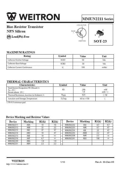
V (BR)CBO 50 50
V (BR)CEO
ON CHARACTERISTICS (Note 2.)
DC Current Gain (VCE= 10 V, IC = 5.0 mA)
MMUN2211 MMUN2212
hFE
35 60
MMUN2213
80
MMUN2214
80
MMUN2215
160
MMUN2216
元器件交易网
Bias Resistor Transistor NPN Silicon
P b Lead(Pb)-Free
MAXIMUM RATINGS
Rating
Collector-Emitter Voltage Collector-Base Voltage Collector Current-Continuous
160
MMUN2230
3.0
MMUN2231
8.0
MMUN2232
15
MMUN2233
80
MMUN2234
80
MMUN2235
80
MMUN2238
160
MMUN2241
160
Collector-Emitter Saturation Voltage (IC = 10 mA, IB = 0.3 mA) (IC= 10 mA, I B = 5 mA) MMUN2230/MMUN2231
Characteristic
Symbol Min
OFF CHARACTERISTICS
Collector-Base Cutof f Current (VCB= 50 V, IE = 0)
ICBO
-
Collector-Emitter Cutoff Current (VCE= 50 V, IB= 0)
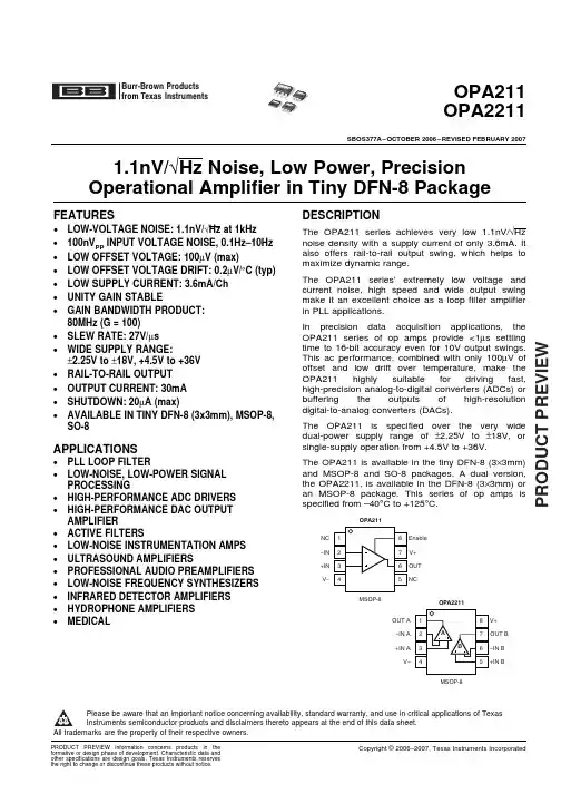
OPA2211中文资料
ü
ü
ห้องสมุดไป่ตู้
ü
ü
ü
ü
ü
ü
ü
ü
ü
ü
ü
ü
PACKAGE DESIGNATOR
DRG DCK
D DRG DCK
DRG DCK
D DRG DCK
PACKAGE MARKING
TBD TBD TBD TBD TBD
TBD TBD TBD TBD TBD
(1) For the most current package and ordering information see the Package Option Addendum at the end of this document, or see the TI web site at .
元器件交易网
PRODUCT PREVIEW
BurrĆBrown Products from Texas Instruments
OPA211
OPA211
OPA2211
OPA2211
OPA211 OPA2211
SBOS377A – OCTOBER 2006 – REVISED FEBRUARY 2007
All trademarks are the property of their respective owners.
PRODUCT PREVIEW information concerns products in the formative or design phase of development. Characteristic data and other specifications are design goals. Texas Instruments reserves the right to change or discontinue these products without notice.
NXP UBA2211 230V 12W CFL演示板用户手册说明书

UM 10418基于UBA2211的230V 12W CFL演示板版本.2.02——2011 01 10 用户手册文档信息摘要该文档为基于UBA2211的12W演示板用户手册修订历史v.1 10101026 第一版1. 简介UBA2211是一款耐高压集成控制芯片,外部只需增加少量的元件,就能驱动和控制紧凑型荧光灯(CFLs)。
它能为灯正常预热、点火和工作提供所必要的功能。
其内部集成了相关必要的保护功能,具有很高的性价比。
该用户手册将介绍基于UBA2211 230V 12W演示板的应用。
2. 特性2.1 系统集成度●集成半桥功率MOSFET- UBA2211A:导通阻抗13.5欧姆:最大点火电流:0.9A- UBA2211B: 导通阻抗0欧姆:最大点火电流1.35A- UBA2211C: 导通阻抗6.6欧姆:最大点火电流:1.85A●集成自举二极管●集成低压供电电路●集成电平转换电路2.2 灯管寿命●可调的预热时间和点火时间●可调的预热电流,不受电源电压影响●支持冷启动,最小辉光放电时间控制●可调灯功率●灯功率不受电源电压变化影响2.3 安全性●安全启动功能● 50%精确占空比●欠电压自锁保护●电感饱和保护●过热保护●电容模式保护● EOL 保护●灯开路保护2.4 应用简单●可调工作频率,方便与各种灯管匹配3. 电路图典型应用电路如图1图1 紧凑型荧光灯典型应用电路4. 规格说明UBA2211演示板用来驱动12W功率的灯管。
规格说明如下所示:● 230V(AC)−输入电压范围:220V到240V;50Hz−输入功率:230V(AC)下12W−输入电流:230V(AC)下80mA−功率因数:>0.58−正常运行频率:42kHz− 800ms的预热时间●灯管− Baishi 3U 12W灯管−其他灯电压70V,电流150mA的灯管5. 实际应用230V(AC)电源输入和灯管四个输出连接如图2所示:图2 12W CFL UBA2211实际应用6. 电路说明UBA2211为一款集成电路控制芯片,用于驱动紧凑型荧光灯。
EG2121大功率MOS管、IGBT管栅极驱动芯片用户手册说明书

版本变更记录目录1. 特性 (1)2. 描述 (1)3. 应用领域 (1)4. 引脚 (2)4.1 引脚定义 (2)4.2 引脚描述 (2)5. 结构框图 (3)6. 典型应用电路 (3)7. 电气特性 (4)7.1 极限参数 (4)7.2 典型参数 (5)7.3 开关时间特性及死区时间波形图 (6)8. 应用设计 (7)8.1 Vcc端电源电压 (7)8.2 输入逻辑信号要求和输出驱动器特性 (7)8.3 自举电路 (8)9. 封装尺寸 (9)9.1 SOP8封装尺寸 (9)EG2121芯片数据手册V1.01. 特性◼高端悬浮自举电源设计,耐压可达200V◼适应5V、3.3V输入电压◼最高频率支持500KHZ◼带VCC欠压保护◼输出电流能力I O+/- 0.8A/1.2A◼内建死区控制电路◼自带闭锁功能,彻底杜绝上、下管输出同时导通◼HIN输入通道高电平有效,控制高端HO输出◼LIN输入通道低电平有效,控制低端LO输出◼外围器件少◼封装形式:SOP8◼无铅无卤符合ROHS标准2. 描述EG2121是一款高性价比的大功率MOS管、IGBT管栅极驱动专用芯片,内部集成了逻辑信号输入处理电路、死区时控制电路、欠压关断电路、闭锁电路、电平位移电路、脉冲滤波电路及输出驱动电路,专用于无刷电机控制器中的驱动电路。
EG2121高端的工作电压可达200V,低端Vcc的电源电压范围宽10V~20V,静态功耗低。
该芯片具有闭锁功能防止输出功率管同时导通,输入通道HIN内部200K下拉电阻和LIN内部上拉到5V,在输入悬空时使上、下功率MOS管处于关闭状态,输出电流能力I O+/- 0.8/1.2A,采用SOP8封装。
3. 应用领域◼移动电源高压快充开关电源◼电动车控制器◼变频水泵控制器◼200V降压型开关电源◼无刷电机驱动器◼高压Class-D类功放4. 引脚4.1 引脚定义图4-1. EG2121管脚定义4.2 引脚描述5. 结构框图LOGNDVccHOVS VB图5-1. EG2121内部电路图6. 典型应用电路+15V+200VOUT图6-1. EG2121典型应用电路图7. 电气特性7.1 极限参数注:超出所列的极限参数可能导致芯片内部永久性损坏,在极限的条件长时间运行会影响芯片的可靠性。
基于UBA2211的简单高性能节能灯镇流器设计
中 图分 类号 : M9 36 T 2 .1
2 2 5 01 年 月
am o
图 1 UBA2 1 2 1芯 片 电 路 组 成 及 其 与 外 部 元 件 连 接
成 了电荷 泵 二极 管 ( 图 1中 D 和 D ) 见 及箝 位 用 齐
纳 二 极 管 ( , 采 用 D P D )而 I 8封 装 的器 件 则 不 含 有
最 大 电 灯 电 流 分 别 为 09A、 .5A 和 18 . 13 .5A。 U A 2 系列 I B 21 1 C可用作设计 7 2 w 的 C L ~5 F 镇流器 。
用户设计低成本高性能 C L镇流器提供 了新 的解 F
决方案。
收 稿 日期 :0 — 9 0 2 1 0— 1 1
一
3 — 7
第1卷 5
第5 期
鼋涤艇瓤 用
P0W ER UPPLY S TECHNOLOGI ESAND APPLI CATI ONS
Vo .5 11 No5 . Ma .2 2 v 01
U A 2 1 T和 U A 2 1 T A、 C 三 种 器 件 半 B 2 1B B 2 1C 。 B、
到 1.V 的启 动 门 限 , 动 电流 源被 切 断 , 荡 器 1 7 启 振
开 始振荡 , 桥进 入到 开关 状态 。只要 半桥 在 I 半 C引
桥晶体管导通 电阻分部是 l. Q、 Q 和 6 3 9 5 . Q, 6
2SK2211资料
Modicon M221 TM221C16R 产品数据手册说明书
TM221C16R.i s c l ai m e r : T h i s d o c u m e n t a t i o n i s n o t i n t e n d e d a s a s u b s t i t u t e f o r a n d i s n o t t o b e u s e d f o r d e t e r m i n i n g s u i t a b i l i t y o r r e l i a b i l i t y o f t h e s e p r o d u c t s f o r s p e c i f i c u s e r a p p l i c a t i o n sProduct datasheetCharacteristicsTM221C16Rcontroller M221 16 IO relayMainRange of productModicon M221Product or component type Logic controller [Us] rated supply voltage 100...240 V ACDiscrete input number 9 discrete input conforming to IEC 61131-2 Type 1Analogue input number 2 at input range: 0...10 V Discrete output type Relay normally open Discrete output number 7 relay Discrete output voltage 5...125 V DC 5...250 V AC Discrete output current2 AComplementaryDiscrete I/O number16Number of I/O expansion module <= 4 for transistor output <= 4 for relay output Supply voltage limits 85...264 V Network frequency 50/60 Hz Inrush current<= 40 APower consumption in VA <= 46 VA at 100...240 V with max number of I/O expansion module <= 31 VA at 100...240 V without I/O expansion module Power supply output current 0.325 A at 5 V for expansion bus 0.12 A at 24 V for expansion bus Discrete input logic Sink or source (positive/negative)Discrete input voltage 24 V Discrete input voltage type DC Analogue input resolution 10 bits LSB value 10 mVConversion time1 ms per channel + 1 controller cycle time for analog input Permitted overload on inputs+/- 30 V DC for analog input with 5 min maximum +/- 13 V DC for analog input permanentVoltage state1 guaranteed>= 15 V for inputCurrent state 1 guaranteed>= 2.6 mA for fast input>= 4.2 mA for discrete inputVoltage state 0 guaranteed<= 5 V for inputCurrent state 0 guaranteed<= 1.3 mA for discrete input<= 0.6 mA for fast inputDiscrete input current7 mA for discrete input5 mA for fast inputInput impedance 4.9 kOhm for fast input3.4 kOhm for discrete input100 kOhm for analog inputResponse time10 ms turn-on operation for output35 µs turn-off operation for input; I2...I5 terminal10 ms turn-off operation for output5 µs turn-on operation for fast input; I0, I1, I6, I7 terminal35 µs turn-on operation for input; other terminals terminal5 µs turn-off operation for fast input; I0, I1, I6, I7 terminal100 µs turn-off operation for input; other terminals terminal Configurable filtering time0 ms for input12 ms for input3 ms for inputOutput voltage limits125 V DC277 V ACCurrent per output common 6 A at COM 1 termnal7 A at COM 0 termnalAbsolute accuracy error+/- 1 % of full scale for analog inputElectrical durability Inductive AC-15, (cos phi = 0.35) 240 V / 120 VA : 100000 cyclesResistive DC-12, 24 V / 48 W : 100000 cyclesResistive AC-12, 120 V / 240 VA : 100000 cyclesInductive AC-15, (cos phi = 0.35) 240 V / 36 VA : 300000 cyclesResistive AC-12, 120 V / 80 VA : 300000 cyclesInductive (L/R = 7 ms) DC-13, 24 V / 24 W : 100000 cyclesResistive DC-12, 24 V / 16 W : 300000 cyclesInductive (L/R = 7 ms) DC-13, 24 V / 7.2 W : 300000 cyclesInductive AC-14, (cos phi = 0.7) 240 V / 240 VA : 100000 cyclesInductive AC-15, (cos phi = 0.35) 120 V / 60 VA : 100000 cyclesInductive AC-14, (cos phi = 0.7) 240 V / 72 VA : 300000 cyclesInductive AC-15, (cos phi = 0.35) 120 V / 18 VA : 300000 cyclesResistive AC-12, 240 V / 480 VA : 100000 cyclesInductive AC-14, (cos phi = 0.7) 120 V / 120 VA : 100000 cyclesResistive AC-12, 240 V / 160 VA : 300000 cyclesInductive AC-14, (cos phi = 0.7) 120 V / 36 VA : 300000 cycles Switching frequency20 switching operations/minute with maximum load Mechanical durability>= 20000000 cycles for relay outputMinimum load 1 mA at 5 V DC for relay outputProtection type Without protection at 5 AReset time 1 sMemory capacity256 kB for user application and data RAM with 10000 instructions256 kB for internal variables RAMData backed up256 kB built-in flash memory for backup of application and data Data storage equipment 2 GB SD card optionalBattery type BR2032 lithium non-rechargeable, battery life: 4 yrBackup time 1 year at 25 °C by interruption of power supplyExecution time for 1 KInstruction0.3 ms for event and periodic taskExecution time per instruction0.2 µs BooleanExct time for event task60 µs response timeMaximum size of object areas512 %M memory bits512 %KW constant words255 %TM timers255 %C counters8000 %MW memory wordsRealtime clock WithClock drift<= 30 s/month at 25 °CRegulation loop Adjustable PID regulator up to 14 simultaneous loopsCounting input number 4 fast input (HSC mode) (counting frequency: 100 kHz), counting capacity: 32 bitsControl signal type Frequency meterSingle phaseDual phase (pulse/direction)Dual phase (quadrature)Integrated connection type USB port with connector mini B USB 2.0Non isolated serial link "serial 1" with connector RJ45 and interface RS485Non isolated serial link "serial 2" with connector RJ45 and interface RS232/RS485Supply Serial serial link supply at 5 V 200 mATransmission rate 1.2...115.2 kbit/s (115.2 kbit/s by default) for bus length of 15 m - communication protocol: RS4851.2...115.2 kbit/s (115.2 kbit/s by default) for bus length of 3 m - communication protocol: RS232480 Mbit/s - communication protocol: USBCommunication port protocol USB port : USB protocol - SoMachine-NetworkNon isolated serial link : Modbus protocol master/slave - RTU/ASCII or SoMachine-Network Local signalling 1 LED green for SD card access (SD)1 LED red for BAT1 LED green for SL11 LED green for SL21 LED per channel green for I/O state1 LED red for module error (ERR)1 LED green for PWR1 LED green for RUNElectrical connection Mini B USB 2.0 connector for a programming terminalTerminal block, 3 terminal(s) for connecting the 24 V DC power supplyConnector, 4 terminal(s) for analogue inputsRemovable screw terminal block for inputsRemovable screw terminal block for outputsCable length<= 10 m shielded cable for fast input<= 30 m unshielded cable for output<= 30 m unshielded cable for digital input<= 1 m unshielded cable for analog inputInsulation2300 V AC between output and internal logicNon-insulated between analogue inputs500 V AC between input and internal logicNon-insulated between analogue input and internal logic1500 V AC between supply and ground500 V AC between sensor power supply and ground500 V AC between input and ground1500 V AC between output and ground2300 V AC between supply and internal logic500 V AC between sensor power supply and internal logic500 V AC between Ethernet terminal and internal logic2300 V AC between supply and sensor power supplyMarking CESensor power supply DC at 250 mA supplied by the controllerMounting support Top hat type TH35-15 rail conforming to IEC 60715Top hat type TH35-7.5 rail conforming to IEC 60715Plate or panel with fixing kitHeight90 mmDepth70 mmWidth95 mmProduct weight0.346 kgEnvironmentStandards EN/IEC 61010-2-201EN/IEC 61131-2EN/IEC 60664-1Product certifications RCMIACS E10DNV-GLcULusCSALRABSEACEnvironmental characteristic Ordinary and hazardous locationResistance to electrostatic discharge 4 kV on contact conforming to EN/IEC 61000-4-28 kV in air conforming to EN/IEC 61000-4-2Resistance to electromagnetic fields10 V/m ( 80 MHz...1 GHz) conforming to EN/IEC 61000-4-33 V/m ( 1.4 GHz...2 GHz) conforming to EN/IEC 61000-4-31 V/m ( 2...2.7 GHz) conforming to EN/IEC 61000-4-3Resistance to magnetic fields 30 A/m at 50...60 Hz conforming to EN/IEC 61000-4-8Resistance to fast transients2 kV for power lines conforming to EN/IEC 61000-4-42 kV for relay output conforming to EN/IEC 61000-4-41 kV for Ethernet line conforming to EN/IEC 61000-4-41 kV for serial link conforming to EN/IEC 61000-4-41 kV for I/O conforming to EN/IEC 61000-4-4Surge withstand2 kV for power lines (AC) in common mode conforming to EN/IEC 61000-4-52 kV for relay output in common mode conforming to EN/IEC 61000-4-51 kV for I/O in common mode conforming to EN/IEC 61000-4-51 kV for shielded cable in common mode conforming to EN/IEC 61000-4-50.5 kV for power lines (DC) in differential mode conforming to EN/IEC 61000-4-51 kV for power lines (AC) in differential mode conforming to EN/IEC 61000-4-51 kV for relay output in differential mode conforming to EN/IEC 61000-4-50.5 kV for power lines (DC) in common mode conforming to EN/IEC 61000-4-5Resistance to conducted disturbances,induced by radio frequency fields10 Vrms (0.15...80 MHz) conforming to EN/IEC 61000-4-63 Vrms (0.1...80 MHz) conforming to Marine specification (LR, ABS, DNV, GL)10 Vrms (spot frequency (2, 3, 4, 6.2, 8.2, 12.6, 16.5, 18.8, 22, 25 MHz)) conforming to Marine specification (LR, ABS, DNV, GL)Electromagnetic emissionConducted emissions conforming to EN/IEC 55011 power lines (AC), 0.15...0.5 MHz : 79 dBμV/m QP/66 dBμV/m AVConducted emissions conforming to EN/IEC 55011 power lines (AC), 0.5...300 MHz : 73 dBμV/m QP/60 dBμV/m AVConducted emissions conforming to EN/IEC 55011 power lines, 10...150 kHz : 120...69 dBµV/m QP Conducted emissions conforming to EN/IEC 55011 power lines, 150 kHz...1.5 MHz : 79...63 dBμV/m QPConducted emissions conforming to EN/IEC 55011 power lines, 1.5...30 MHz : 63 dBμV/m QP Radiated emissions conforming to EN/IEC 55011 class A 10 m, 30...230 MHz : 40 dBμV/m QP Radiated emissions conforming to EN/IEC 55011 class A 10 m, 200 MHz...1 GHz : 47 dBμV/m QP Immunity to microbreaks10 msAmbient air temperature for operation -10...55 °C for horizontal installation -10...35 °C for vertical installation Ambient air temperature for storage -25...70 °CRelative humidity 10...95 % without condensation in operation 10...95 % without condensation in storage IP degree of protection IP20 with protective cover in place Pollution degree <= 2Operating altitude 0...2000 m Storage altitude 0...3000 mVibration resistance3.5 mm (vibration frequency: 5...8.4 Hz) on symmetrical rail 1 gn (vibration frequency: 8.4...150 Hz) on symmetrical rail 3.5 mm (vibration frequency:5...8.4 Hz) on panel mounting 1 gn (vibration frequency: 8.4...150 Hz) on panel mounting Shock resistance98 m/s² (test wave duration:11 ms)Offer SustainabilitySustainable offer status Green Premium productRoHS (date code: YYWW)Compliant - since 1415 - Schneider Electric declaration of conformity Schneider Electric declaration of conformity REAChReference not containing SVHC above the threshold Reference not containing SVHC above the threshold Product environmental profileAvailableProduct environmental Product end of life instructionsAvailableEnd of life manualProduct datasheetTM221C16R Dimensions DrawingsDimensionsProduct datasheetTM221C16R Mounting and ClearanceMounting on a RailProduct datasheetMounting and ClearanceTM221C16RDirect Mounting on a Panel Surface(1)Install a mounting stripMounting Hole LayoutProduct datasheetTM221C16R Mounting and ClearanceMountingCorrect Mounting PositionAcceptable Mounting PositionIncorrect Mounting PositionProduct datasheetTM221C16R Mounting and ClearanceClearanceDigital InputsWiring Diagram (Positive Logic)(*)Type T fuseWiring Diagram (Negative Logic)(*)Type T fuseConnection of the Fast InputsI0, I1, I6, I7Relay OutputsNegative Logic (Sink)(*)Type T fuse(1)The COM1 and COM2 terminals are not connected internally.(2)To improve the life time of the contacts, and to protect from potential inductive load damage, you must connect a free wheeling diode in parallel to each in B Sink wiring (negative logic)Positive Logic (Source)(*)Type T fuse(1)The COM1 and COM2 terminals are not connected internally.(2)To improve the life time of the contacts, and to protect from potential inductive load damage, you must connect a free wheeling diode in parallel to each in A Source wiring (positive logic)Analog InputsUSB Mini-B ConnectionSL1 ConnectionSL1N.C.: not connected* : 5 Vdc delivered by the controller. Do not connect.SL2 ConnectionN.C.: not connectedPerformance CurvesDerating CurvesEmbedded Digital Inputs (No Cartridge)X :Ambient temperatureY :Input simultaneous ON ratioEmbedded Digital Inputs (with Cartridge)X :Ambient temperatureY :Input simultaneous ON ratioTM221C16R.。
OB2211, OB2212 Datasheet
GENERAL DESCRIPTIONOB2211/OB2212 series is an offline PWM Power switch for low power AC/DC charger and adaptor applications. It operates in primary-side sensing and regulation, thus, opto-coupler and TL431 is eliminated. It achieves excellent Constant Voltage (CV) and Constant Current (CC) performance by built-in constant current and constant voltage control, as shown in the figure below. OB2211/OB2212 operates with flyback converter in DCM mode. The pulse frequency modulation (PFM) is used in CC control. In CV control, multi-mode operations are utilized to achieve high performance and efficiency: fixed frequency mode at large load conditions; frequency reduction mode atlight/medium load; ‘Extended burst mode’ atNo/light load. OB2211/OB2212 offers complete protection coverage with auto-recovery features including Cycle-by-Cycle current limiting, VDD over-voltage clamp and UVLO, and Power on soft start. Excellent EMI performance is achieved with On-Bright proprietary frequency shuffling technique together with soft switching control at the totem pole gate FEATURESPrimary-side Sensing and Regulation WithoutTL431 and Opto-couplerMulti-mode Operation for High Efficiency Programmable CV and CC RegulationFrequency Shuffling and Adjustable Gate Drive Greatly Improving EMIPower on Soft-start Time (4ms)“Extended Burst Mode Control” for Improved Efficiency and Minimum Standby Design Built-in Leading Edge Blanking Cycle-by-Cycle Current LimitingVDD Under Voltage Lockout with Hysteresis (UVLO)Gate Output Maximum Voltage Clamp (16V) Auto-restart in Short Circuit APPLICATIONSLow Power AC/DC offline SMPS for Cell Phone ChargerDigital Cameras Charger Small Power AdaptorAuxiliary Power for PC, TV etc. Linear Regulator/RCC Replacement OB2211 is offered in SOP8 package.OB2212 is offered in DIP8 packageTYPICAL APPLICATIONGENERAL INFORMATION Pin ConfigurationOB2211 is offered in SOP8OB2212 is offered in DIP8The pin map is shown as below.Ordering InformationPart Number DescriptionOB2211CP SOP8,Pb-freeOB2211CPA SOP8, Pb-free, T&ROB2212AP DIP8,Pb-freeNote: All Devices are offered in Pb-free Package if not otherwisenoted.Package Dissipation RatingPackage RθJA (°C/W)SOP8 150DIP8 90Absolute Maximum RatingsParameter ValueDrain Voltage (off state)-0.3V to 650VVDD Voltage -0.3 to 38 VVDDG Voltage -0.3 to 38 VVDD Zener Clamp ContinuousCurrent10 mACS Input Voltage-0.3 to 7VINV Input Voltage-0.3 to 7VMin/Max Operating JunctionTemperature T J-20 to 150 o CMin/Max Storage TemperatureT stg-55 to 150 oCLead Temperature (Soldering,10secs)260 oCNote: Stresses beyond those listed under “absolute maximumratings” may cause permanent damage to the device. These arestress ratings only, functional operation of the device at these orany other conditions beyond those indicated under “recommendedoperating conditions” is not implied. Exposure to absolutemaximum-rated conditions for extended periods may affect devicereliability.Marking InformationTERMINAL ASSIGNMENTSPin Num Pin Name I/O Description1 VDDG P Internal Gate Driver Power Supply2 VDD P IC DC power supply Input3 INV I Inverting input of error amplifier (EA). Connected to resistor divider fromprimary sensing winding reflecting output voltage. PWM duty cycle isdetermined by EA output and current sense signal at pin 4.4 CS I Current sense input5/6 Drain O HV MOSFET Drain Pin. The Drain pin is connected to the primary lead ofthe transformerGround8 GND POutput Power Table230VAC±15% 90-264VAC ProductOpen Frame1 Open Frame1OB2211 10W 8WOB2212 20W 12W Notes:1. Maximum practical continuous power in an open frame design with sufficient drain pattern as a heat sink, at 50℃ ambient.BLOCK DIAGRAMRECOMMENDED OPERATING CONDITIONSymbol Parameter Min Max UnitVoltage 12 23 V VDD VDDSupplyT A Operating Ambient Temperature -20 85 o CELECTRICAL CHARACTERISTICS(T A = 25O C , VDD=VDDG=16V, if not otherwise noted)Symbol Parameter Test Conditions Min Typ Max Unit Supply Voltage (VDD) Section I DD ST Standby current Start up current, VDD=13V 5 10 uAI DD op Operation Current Operation supply current INV=1.25V, CS=0V, VDD=VDDG=20V- 1.02.0 mA UVLO(ON) VDD Under Voltage Lockout Enter7.5 8.5 10.0 VUVLO(OFF) VDD Under Voltage Lockout Out13.5 14.7 16.0 VV DD _clamp I DD =10mA 38 V Current Sense Input SectionT LEB LEB time 540 ns Vth_oc V TH _OC_test800 830 860 mV Td_oc Propagation delay 150 ns Z SENSE _IN Input Impedance 50 Kohm T_ss Soft start time 4 ms Oscillator Section (CV) Fosc normal mode frequency48 50 52 KHz Fosc_Burst Green-Mode min.Frequency22 KHz△f/FoscFrequency shuffling range+/-4 % CC Section VDD=16V VDDG=16V INV=0V (minimum frequen 12.2 KHz VDD=16V VDDG=16V INV=0.35V 14.7 KHz VDD=16V VDDG=16V INV=0.53V 22.1 KHz VDD=16V VDDG=16V INV=0.71V 29.3 KHzVDD=16V VDDG=16V INV=0.89V36.4 KHz VDDH=16V VDDG=16V INV=1.07V43.2 KHz FccOscillation Frequency VDDH=16V VDDG=16V INV=1.25V50.1 KHz Error Amplifier section Vref_EA Reference voltage for EA1.23 1.25 1.27 VGdc DC gain of the EA 50 dB GBW Unity gain bandwidth 10 kHz Power MOSFET SectionOB2211 650BVdss MOSFET Drain-Source Breakdown VoltageOB2212 600V OB2211 12 15RDS(on) Static Drain to Source On Resistance OB2212 9.9 12 ΏCHARACTERIZATION PLOTSOPERATION DESCRIPTIONOB2211 and OB2212 are cost effective PWM Switch optimized for off-line low power switching mode power supply applications including battery chargers and AC adaptors in sub 20W range. It operates in primary side sensing and regulation, thus opto-coupler and TL431 are not required. Proprietary CC control and built-in error amplifier can achieve a good CC/CV performance.z Startup Current and Start up ControlStartup current of OB2211/2 is designed to be very low so that VDD could be charged up above UVLO threshold level and device starts up quickly. A large value startup resistor can therefore be used to minimize the power loss yet reliable startup in application. For AC/DC adaptor with universal input range design, a 1.2 M Ω, 1/8 W startup resistor could be used together with a VDD capacitor to provide a fast startup and yet low power dissipation design solution.z Operating CurrentThe Operating current of OB2211/2 is as low as 1mA. Good efficiency is achieved with the low operating current together with ‘Extended burst mode’ control features.z Soft StartOB2211/2 features an internal 4ms soft start to soften the electrical stress occurring in the power supply during startup. It is activated during the power on sequence. As soon as VDD reaches UVLO(OFF), the peak current is gradually increased from nearly zero to the maximum clamping level 0.77V. Every restart is followed by a soft start.z CC/CV OperationOB2211/2 is designed to produce an approximate CV/CC output characteristic as shown in the figure 1. In charger applications, a discharged batteryoperates on the CC portion of the curve until almost fully charged and then smoothly switches to the CVportion of the curve. In an AC adapter, the normal operation occurs only on the CV portion of the curve, the CC portion provides over current protection and auto-restart short circuit protection. In CV operation, the output voltage is sensed on the primary side and the sensed signal controls the duty cycle through a built-in error amplifier (EA).Figure 1z Error Amplifier (EA)Connected to a resistor divider from the primary side sensing winding, the inverting input of the Error Amplifier (EA) is compared to an internal reference voltage of 1.25V to regulate the output voltage. The EA output is internally connected to the PWM generator and controls the duty cycle.z Primary Side Sensing and RegulationFigure 2 shows the simplified schematic of Flyback converter using primary side sensing and regulation. The voltage signal reflecting the output voltage from a feedback winding in the primary side is used to monitor and regulate the output voltage. The relationship of the DC voltage of the feedback winding and the output voltage is expressed as:()21F F o FB V V V N V −+⋅= (1)Where N is the turn ratio between the feedback winding and the output winding, V F1 is the forward drop voltage of the rectified diode, D1, and V F2is the forward drop voltage of the rectified diode, D2.FB INV V R R R V ⋅+=212(2)()()21212F F o V V V N R R R Vo −+⋅⋅+=(3)Figure 2In the regulation, V INV is regulated to 1.25V. V F1 of Diode D1 changes with the output current thus the load conditions, and V F2 is always constant regardless of output current, therefore, the regulation of output voltage, Vo, is affected by V F1 as shown in equation 3. To reduce the nonlinear effect of V F1, the N ratio needs is chosen to be small.z Loop CompensationTo provide good line and load regulation and dynamic response, a capacitor used for loop compensation is connected to pin INV as shown in Figure 3,where Req, Ceq and Roeq is respectively reflected effective ESR resistance, output capacitance and load resistance from the output winding to the primary side winding. The resistance Req and capacitance Ceq form a zero. The resistance Roeq and capacitance Ceq form a pole. The small signal transfer function of EA compensation circuit is obtained by:()1211221211C R R s C R s R R R A v v FBC +++⋅+⋅=ΛΛ(4)z Constant Current (CC) ModeTo achieve constant current (CC) at different output voltage, the Flyback converter is designed to operate in DCM mode and the switching frequency changes with output voltage as INV s V k f ⋅= and it is low clamped to12KHz, therefore the switching frequency is proportional to the output voltage as V INV is approximately the replica of output voltage, Vo .Figure 4 illustrates the key waveforms of the Flyback converter operating in discontinuous current mode (DCM). During Q1 on-time, theenergy can be stored in the primary inductor of the transformer; the load current is supplied from the output capacitor. The peak current of the primary side ramps up to I PK at the end of the on-time:on minpk T L V I ⋅=(5) In OB2211/2, the peak current at CC mode is always constant regardless of voltage level of V INV . The energy stored in the primary inductance Lm at the end of Ton is expressed by the current Ipk:()22pk m I L E ⋅=(6)where RsV I oc th pk _=, Rs is the current sensingresistor connecting to pin CS.During Q1 turns off, the energy stored in the primary winding is transferred to the secondary and output. The power drawn from the input AC supply is expressed by:()22pk s m I f L P ⋅⋅=(7)Assuming 100% efficiency, we can get the following equation at different output voltage,()o o pk s m I V I f L ×=⋅⋅⋅22(8)The output current is further expressed as()022V I f L I pk s m o ×⋅⋅⋅=(9)Since fs is linear proportional to Vo as described, therefore output current Io is kept constant and it depends only on L m and I pk .Fig. 4 The waveforms of Flyback converter in DCMz Extended Burst Mode OperationAt light load or zero load condition, most of the power dissipation in a switching mode power supply is from switching loss, the core loss of the transformer and the loss on the snubber circuit. The magnitude of power loss is in proportion to the switching frequency. Lower switching frequency leads to the reduction on the power loss and thus conserves the energy.OB2211/2 self adjusts the switching frequency according to the loading condition. The switch frequency is reduced at light/no load condition to improve the conversion efficiency. At light load/no load condition, the output of the Error amplifier (EA) drops below the burst mode threshold level and device enters Burst Mode control. The frequency control also eliminates the audio noise at any loading conditions.z Oscillator OperationThe switching frequency of OB2211/2 is internally fixed at 50KHZ. No external frequency setting components are required for PCB design simplification.z Frequency shuffling for EMI improvement The frequency Shuffling/jittering (switching frequency modulation) is implemented in OB2211/2. The oscillation frequency is modulated with a pseudo random source so that the tone energy is spread out. The spread spectrum minimizes the conduction band EMI and therefore eases the system design.z Current Sensing and Leading Edge BlankingCycle-by-Cycle current limiting is offered in OB2211/2 current mode PWM control. The switch current is detected by a sense resistor into the CS pin. An internal leading edge blanking circuit chops off the sensed voltage spike at initial internal power MOSFET on state due to snubber diode reverse recovery and surge gate current of internal power MOSFET so that the external RC filtering on sense input is no longer needed. The current limiting comparator is disabled and cannot turn off the internal power MOSFET during the blanking period. The PWM duty cycle is determined by the current sense input voltage and the EA output voltage.z DriveThe internal power MOSFET in OB2211/2 is driven by a dedicated gate driver for power switch control. Too weak the gate drive strength results in higher conduction and switch loss of MOSFET while too strong gate drive results the compromise of EMIA good tradeoff is achieved through the built-in totem pole gate design with right output strength and dead time control. The low idle loss and good EMI system design is easier to achieve with this dedicated control scheme.In addition to the gate drive control scheme mentioned, the gate drive strength can also be adjusted externally by a resistor connected between VDD and VDDG, the falling edge of the Drain output can be well controlled. It provides great flexibility for system EMI design.z Protection ControlGood power supply system reliability is achieved with its rich protection features including Cycle-by-Cycle current limiting (OCP), and VDD over voltage clamp, Power on Soft Start, Under Voltage Lockout on VDD (UVLO).With On-Bright Proprietary technology, the OCP is line voltage compensated to achieve constant output power limit over the universal input voltage range.VDD is supplied by transformer auxiliary winding output. It is clamped when VDD is higher than 30V. The output of OB2211 is shut down when VDD drops below UVLO(ON) limit and Switcher enters power on start-up sequence thereafter.PACKAGE MECHANICAL DATADimensions In Millimeters Dimensions In Inches SymbolMin Max Min MaxA 1.350 1.750 0.053 0.069A1 0.100 0.250 0.004 0.010 A2 1.300 1.550 0.051 0.061b 0.330 0.510 0.013 0.020c 0.170 0.250 0.006 0.010D 4.700 5.150 0.185 0.203E 3.800 4.000 0.150 0.157E1 5.800 6.200 0.228 0.244e 1.270 (BSC) 0.050 (BSC)L 0.400 1.270 0.016 0.050 θ 0º 8º 0º 8ºDimensions In Millimeters Dimensions In InchesSymbolMin Max Min MaxA 3.710 4.310 0.146 0.1700.500 0.020 A1A2 3.200 3.600 0.126 0.142B 0.350 0.650 0.014 0.026 B1 1.524 (BSC) 0.060 (BSC)C 0.200 0.360 0.008 0.014D 9.000 9.500 0.354 0.374E 6.200 6.600 0.244 0.260 E1 7.320 7.920 0.288 0.312e 2.540 (BSC) 0.100 (BSC)L 3.000 3.600 0.118 0.142 E2 8.200 9.000 0.323 0.354IMPORTANT NOTICERIGHT TO MAKE CHANGESOn-Bright Electronics Corp. reserves the right to make corrections, modifications, enhancements, improvements and other changes to its products and services at any time and to discontinue any product or service without notice. Customers should obtain the latest relevant information before placing orders and should verify that such information is current and complete.WARRANTY INFORMATIONOn-Bright Electronics Corp. warrants performance of its hardware products to the specifications applicable at the time of sale in accordance with its standard warranty. Testing and other quality control techniques are used to the extent it deems necessary to support this warranty. Except where mandated by government requirements, testing of all parameters of each product is not necessarily performed.On-Bright Electronics Corp. assumes no liability for application assistance or customer product design. Customers are responsible for their products and applications using On-Bright’s components, data sheet and application notes. To minimize the risks associated with customer products and applications, customers should provide adequate design and operating safeguards.LIFE SUPPORTOn-Bright Electronics Corp.’s products are not designed to be used as components in devices intended to support or sustain human life. On-bright Electronics Corp. will not be held liable for any damages or claims resulting from the use of its products in medical applications.MILITARYOn-Bright Electronics Corp.’s products are not designed for use in military applications. On-Bright Electronics Corp. will not be held liable for any damages or claims resulting from the use of its products in military applications.。