AT27LV020A-12JU;中文规格书,Datasheet资料
AT27C020中文资料
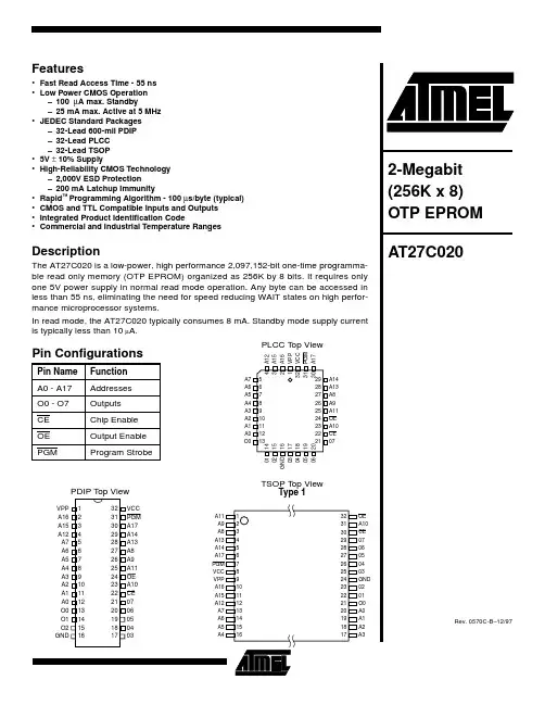
The AT27C020 is available in a choice of industry standard JEDEC-approved one-time programmable (OTP) plastic PDIP, PLCC, and TSOP packages. All devices feature two-line control (CE, OE) to give designers the flexibility to pre-vent bus contention.With 256K byte storage capability, the AT27C020 allows firmware to be stored reliably and to be accessed by the system without the delays of mass storage media. Atmel’s 27C020 have additional features to ensure high quality and efficient production use. The Rapid™Program-ming Algorithm reduces the time required to program the part and guarantees reliable programming. Programming time is typically only 100 µs/byte. The Integrated Product Identification Code electronically identifies the device and manufacturer. This feature is used by industry standard programming equipment to select the proper programming algorithms and voltages.System ConsiderationsSwitching between active and standby conditions via the Chip Enable pin may produce transient voltage excursions. Unless accommodated by the system design, these tran-sients may exceed data sheet limits, resulting in device non-conformance. At a minimum, a 0.1 µF high frequency, low inherent inductance, ceramic capacitor should be uti-lized for each device. This capacitor should be connected between the V CC and Ground terminals of the device, as close to the device as possible. Additionally, to stabilize the supply voltage level on printed circuit boards with large EPROM arrays, a 4.7 µF bulk electrolytic capacitor should be utilized, again connected between the V CC and Ground terminals. This capacitor should be positioned as close as possible to the point where the power supply is connected to the array.Block DiagramAbsolute Maximum Ratings*T emperature Under Bias.......................-55°C to +125°C *NOTICE:Stresses beyond those listed under “Absolute Maximum Ratings” may cause permanent damage to the device. This is a stress rating only and functional operation of the device at these or any other conditions beyond those indicated in the operational sections of this specification is not implied. Exposure to abso-lute maximum rating conditions for extended periods may affect device reliability.Note:1.Minimum voltage is -0.6V DC which mayundershoot to -2.0V for pulses of less than 20 ns. Maximum output pin voltage is V CC + 0.75V DC which may overshoot to +7.0V for pulses of less than 20 ns.Storage T emperature............................-65°C to +150°C Voltage on Any Pin withRespect to Ground...............................-2.0V to +7.0V (1)Voltage on A9 withRespect to Ground ............................-2.0V to +14.0V (1)V PP Supply Voltage withRespect to Ground.............................-2.0V to +14.0V (1)Operating ModesNotes:1.X can be V IL or V IH.2.Refer to Programming Characteristics.3.V H = 12.0 ± 0.5V .4.T wo identifier bytes may be selected. All Ai inputs are held low (V IL ), except A9 which is set to V H and A0 which is toggledlow (V IL ) to select the Manufacturer’s Identification byte and high (V IH ) to select the Device Code byte.Mode/Pin CE OE PGM Ai V PP Outputs ReadV IL V IL X (1)Ai X D OUT Output Disable X V IH X X X HighZ Standby V IH X X X X High Z Rapid Program (2)V IL V IH V IL Ai V PP D IN PGM Verify V IL V IL V IH Ai V PP D OUT PGM InhibitV IH X X X V PP High Z Product Identification (4)V ILV ILXA9 = V H (3)A0 = V IH or V IL A1 - A17 = V ILXIdentification CodeAC Characteristics for Read OperationNote:1.2, 3, 4, 5. See AC Waveforms for Read Operation diagram.Symbol ParameterAT27C020Units -55-70-90-12-15Condition Min Max MinMax MinMax MinMax MinMax t ACC (3)Address to Output Delay CE =OE = V IL 557090120150ns t CE (2)CE to Output Delay OE = V IL 557090120150ns t OE (2)(3)OE to Output Delay CE = V IL2030353540ns t DF(4)(5)OE or CE High to Output Float,whichever occurred first 1820203040nst OH Output Holdfrom Address,CE or OE,whichever occurred first77000nsDC and AC Operating Conditions for Read OperationAT27C020-55-70-90-12-15Operating T emperature (Case)Com.0°C - 70°C 0°C - 70°C 0°C - 70°C 0°C - 70°C 0°C - 70°C Ind.-40°C - 85C -40°C - 85C -40°C - 85C -40°C - 85C -40°C - 85C V CC Power Supply5V ± 10%5V ± 10%5V ± 10%5V ± 10%5V ± 10%DC and Operating Characteristics for Read OperationNotes:1.V CC must be applied simultaneously or before V PP , and removed simultaneously or after V PP .2.V PP may be connected directly to V CC except during programming. The supply current would then be the sum of I CC and I PP .Symbol Parameter ConditionMinMax Units I LI Input Load Current V IN = 0V to V CC (Com., Ind.)±1.0µA I LO Output Leakage Current V OUT = 0V to V CC (Com., Ind.)±5.0µA I PP (2)V PP (1) Read/Standby Current V PP = V CC±10µA I SB V CC (1) Standby Current I SB1 (CMOS), CE = V CC ± 0.3V 100µA I SB2 (TTL), CE = 2.0 to V CC + 0.5V 1.0mA I CC V CC Active Current f = 5 MHz, I OUT = 0 mA, CE = V IL25mA V IL Input Low Voltage -0.60.8V V IH Input High Voltage 2.0V CC + 0.5V V OL Output Low Voltage I OL = 2.1 mA 0.4V V OH Output High VoltageI OH = -400 µA2.4VAC Waveforms for Read Operation (1)Notes: 1.Timing measurement references are 0.8V and 2.0V . Input AC drive levels are 0.45V and 2.4V , unless otherwise specified.2.OE may be delayed up to t CE - t OE after the falling edge of CE without impact on t CE.3.ACC - t OE after the address is valid without impact on t ACC .4.This parameter is only sampled and is not 100% tested.5.Output float is defined as the point when data is no longer driven.Input Test Waveforms and Measurement LevelsFor -55 devices only:t R , t FFor -70,-90,-12,-15 devices only:t R , t F < 20 ns (10% to 90%)Pin Capacitancef = 1 MHz, T = 25°C (1)Note:1.T ypical values for nominal supply voltage. This parameter is only sampled and is not 100% tested.TypMax Units Conditions C IN 48pF V IN = 0V C OUT812pFV OUT = 0VOutput Test Load (1)Note: 1.CL = 100 pF including jig capacitance except -55 devices where CL = 30 pF.Programming Waveforms (1)Notes: 1.The Input Timing reference is 0.8V for V IL and 2.0V for V IH.2.t OE and t DFP are characteristics of the device but must be accommodated by the programmer.3.When programming the A T27C020, a 0.1 µF capacitor is required across V PP and ground to suppress voltage transients.DC Programming CharacteristicsT A = 25 ± 5°C, V CC = 6.5 ± 0.25V, V PP = 13.0 ± 0.25VSymbol Parameter Test ConditionsLimitsUnits Min MaxI LI Input Load Current V IN = V IL, V IH±10µA V IL Input Low Level-0.60.8V V IH Input High Level 2.0VCC+ 1.0V V OL Output Low Voltage I OL = 2.1 mA0.4V V OH Output High Voltage I OH = -400 µA 2.4V I CC2V CC Supply Current (Program and Verify)40mA I PP2V PP Supply Current CE = PGM = V IL20mA V ID A9 Product Identification Voltage11.512.5VAC Programming CharacteristicsT A = 25 ± 5°C, V CC = 6.5 ± 0.25V,V PP = 13.0 ± 0.25VNotes:1.V CC must be applied simultaneously or before V PP and removed simultaneously or after V PP .2.This parameter is only sampled and is not 100% tested. Output Float is defined as the point where data is no longer driven— see timing diagram.3.Program Pulse width tolerance is 100 µs ± 5%.Symbol ParameterTest Condition (1)LimitsUnits Min Max t AS Address Setup Time Input Rise and Fall Times:(10% to 90%) 20 ns.Input Pulse Levels:0.45V to 2.4V Input Timing Reference Level:0.8V to 2.0V Output Timing Reference Level:0.8V to 2.0V2µs t CES CE Setup Time 2µs t OES OE Setup Time 2µs t DS Data Setup Time 2µs t AH Address Hold Time 0µs t DH Data Hold Time2µst DFP OE High to Output Float Delay (2)0130ns t VPS V PP Setup Time 2µs t VCS V CC Set up Time2µs t PW PGM Program Pulse Width (3)95105µs t OE Data Valid from OE150ns t PRTV PP Pulse Rise Time During Programming50nsAtmel’s 27C020 Integrated Product Identification CodePinsCodes A0O7O6O5O4O3O2O1O0Hex DataManufacturer 0000111101E Device T ype111186Rapid Programming AlgorithmA 100 µs PGM pulse width is used to program. The address is set to the first location. V CC is raised to 6.5V and V PP is raised to 13.0V. Each address is first programmed with one 100 µs PGM pulse without verification. Then a verification / reprogramming loop is executed for each address. In the event a byte fails to pass verification, up to 10 successive 100 µs pulses are applied with a verification after each pulse. If the byte fails to verify after 10 pulses have been applied, the part is considered failed. After the byte verifies properly, the next address is selected until all have been checked. V PP is then lowered to 5.0V and V CC to 5.0V. All bytes are read again and compared with the origi-nal data to determine if the device passes or fails.Ordering Informationt ACC (ns)I CC (mA)Ordering Code Package Operation Range Active Standby55250.1A T27C020-55JCA T27C020-55PCA T27C020-55TC 32J32P632TCommercial(0°C to 70°C)250.1A T27C020-55JIA T27C020-55PIA T27C020-55TI 32J32P632TIndustrial(-40°C to 85°C)70250.1A T27C020-70JCA T27C020-70PCA T27C020-70TC 32J32P632TCommercial(0°C to 70°C)250.1A T27C020-70JIA T27C020-70PIAT27C020-70TI 32J32P632TIndustrial(-40°C to 85°C)90250.1A T27C020-90JCA T27C020-90PCA T27C020-90TC 32J32P632TCommercial(0°C to 70°C)250.1A T27C020-90JIA T27C020-90PIAT27C020-90TI 32J32P632TIndustrial(-40°C to 85°C)120250.1A T27C020-12JCA T27C020-12PCA T27C020-12TC 32J32P632TCommercial(0°C to 70°C)250.1A T27C020-12JIA T27C020-12PIA T27C020-12TI 32J32P632TIndustrial(-40°C to 85°C)150250.1A T27C020-15JCA T27C020-15PCA T27C020-15TC 32J32P632TCommercial(0°C to 70°C)250.1A T27C020-15JIA T27C020-15PIA T27C020-15TI 32J32P632TIndustrial(-40°C to 85°C)Package Type32J32-Lead,Plastic J-Leaded Chip Carrier (PLCC)32P632-Lead, 0.600" Wide, Plastic Dual Inline Package (PDIP) 32T32-Lead, Plastic Thin Small Outline Package (TSOP)。
AT28LV010-20TU中文资料
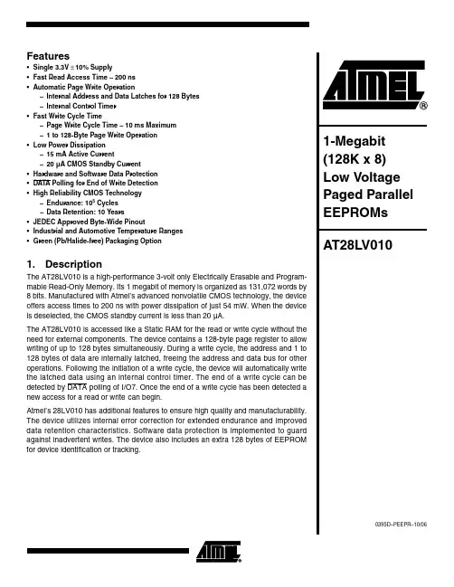
Features Array•Single 3.3V ± 10% Supply•Fast Read Access Time – 200 ns•Automatic Page Write Operation–Internal Address and Data Latches for 128 Bytes–Internal Control Timer•Fast Write Cycle Time–Page Write Cycle Time – 10 ms Maximum–1 to 128-Byte Page Write Operation•Low Power Dissipation–15 mA Active Current–20µA CMOS Standby Current•Hardware and Software Data Protection•DATA Polling for End of Write Detection•High Reliability CMOS Technology–Endurance: 105 Cycles–Data Retention: 10 Years•JEDEC Approved Byte-Wide Pinout•Industrial and Automotive Temperature Ranges•Green (Pb/Halide-free) Packaging Option1.DescriptionThe AT28LV010 is a high-performance 3-volt only Electrically Erasable and Program-mable Read-Only Memory. Its 1 megabit of memory is organized as 131,072 words by 8 bits. Manufactured with Atmel’s advanced nonvolatile CMOS technology, the device offers access times to 200 ns with power dissipation of just 54 mW. When the device is deselected, the CMOS standby current is less than 20µA.The AT28LV010 is accessed like a Static RAM for the read or write cycle without the need for external components. The device contains a 128-byte page register to allow writing of up to 128 bytes simultaneously. During a write cycle, the address and 1 to 128 bytes of data are internally latched, freeing the address and data bus for other operations. Following the initiation of a write cycle, the device will automatically write the latched data using an internal control timer. The end of a write cycle can benew access for a read or write can begin.Atmel’s 28LV010 has additional features to ensure high quality and manufacturability. The device utilizes internal error correction for extended endurance and improved data retention characteristics. Software data protection is implemented to guard against inadvertent writes. The device also includes an extra 128 bytes of EEPROMfor device identification or tracking.2.Pin Configurations2.132-lead PLCC Top ViewPin Name Function A0 - A16Addresses CE Chip Enable OE Output Enable WE Write Enable I/O0 - I/O7Data Inputs/Outputs NC No Connect DCDon’t Connect2.232-lead PDIP Top View2.332-lead TSOP Top View3.Block Diagram4.Device Operation4.1Readdata stored at the memory location determined by the address pins is asserted on the outputs.control gives designers flexibility in preventing bus contention in their system.4.2WriteThe write operation of the AT28LV010 allows 1 to 128 bytes of data to be written into thedevice during a single internal programming period. Each write operation must be preceded bythe software data protection (SDP) command sequence. This sequence is a series of threeunique write command operations that enable the internal write circuitry. The commandsequence and the data to be written must conform to the software protected write cycle timing.Addresses are latched on the falling edge of WE or CE, whichever occurs last and data iswritten within 150 µs (t BLC) of the previous byte. If the t BLC limit is exceeded the AT28LV010will cease accepting data and commence the internal programming operation. If more thanone data byte is to be written during a single programming operation, they must reside on theduring the page write operation, A7 - A16 must be the same.The A0 to A6 inputs are used to specify which bytes within the page are to be written. Thebytes may be loaded in any order and may be altered within the same load period. Only byteswhich are specified for writing will be written; unnecessary cycling of other bytes within thepage does not occur.4.3page write cycle an attempted read of the last byte written will result in the complement of thewritten data to be presented on I/O7. Once the write cycle has been completed, true data isvalid on all outputs, and the next write cycle may begin. DATA Polling may begin at anytimeduring the write cycle.4.4Toggle BitIn addition to DATA Polling the AT28LV010 provides another method for determining the endof a write cycle. During the write operation, successive attempts to read data from the devicewill result in I/O6 toggling between one and zero. Once the write has completed, I/O6 will stoptoggling and valid data will be read. Reading the toggle bit may begin at any time during thewrite cycle.4.5Data ProtectionIf precautions are not taken, inadvertent writes may occur during transitions of the host systempower supply. Atmel® has incorporated both hardware and software features that will protectthe memory against inadvertent writes.4.5.1Hardware ProtectionHardware features protect against inadvertent writes to the AT28LV010 in the following ways:(a) V CC power-on delay – once V CC has reached 2.0V (typical) the device will automaticallytime out 5 ms (typical) before allowing a write; (b) write inhibit – holding any one of OE low, CEthe WE or CE inputs will not initiate a write cycle.4.5.2Software Data ProtectionThe AT28LV010 incorporates the industry standard software data protection (SDP) function.Unlike standard 5-volt only EEPROM’s, the AT28LV010 has SDP enabled at all times. There-fore, all write operations must be preceded by the SDP command sequence.The data in the 3-byte command sequence is not written to the device; the addresses in thecommand sequence can be utilized just like any other location in the device. Any attempt towrite to the device without the 3-byte sequence will start the internal timers. No data will bewritten to the device. However, for the duration of t WC, read operations will effectively be poll-ing operations.AT28LV010Notes:1.X can be V IL or V IH .2.Refer to AC Programming Waveforms.5.DC and AC Operating RangeAT28LV010-20AT28LV010-25OperatingT emperature (Case)Ind.-40°C - 85°C -40°C - 85°CAutomotive-40°C - 125°C V CC Power Supply3.3V ± 5%3.3V ± 10%6.Operating ModesMode CE OE WE I/O Read V IL V IL V IH D OUT Write (2)V IL V IH V IL D IN Standby/Write Inhibit V IH X (1)X High ZWrite Inhibit X X V IH Write Inhibit X V IL X Output Disable XV IHXHigh Z 7.Absolute Maximum Ratings*T emperature Under Bias................................-55°C to +125°C *NOTICE:Stresses beyond those listed under “Absolute Maximum Ratings” may cause permanent dam-age to the device. This is a stress rating only and functional operation of the device at these or any other conditions beyond those indicated in the operational sections of this specification is not implied. Exposure to absolute maximum rating conditions for extended periods may affect device reliabilityStorage T emperature.....................................-65°C to +150°C All Input Voltages (including NC Pins)with Respect to Ground...................................-0.6V to +6.25V All Output Voltageswith Respect to Ground.............................-0.6V to V CC + 0.6V Voltage on OE and A9with Respect to Ground...................................-0.6V to +13.5V8.DC CharacteristicsSymbol Parameter Condition MinMax Units I LI Input Load Current V IN = 0V to V CC 1µA I LO Output Leakage Current V I/O = 0V to V CC1µA I SB V CC Standby Current CMOS CE = V CC - 0.3V to V CC + 1VInd.50µA I CC V CC Active Current f = 5 MHz; I OUT = 0 mA; V CC = 3.6V15mA V IL Input Low Voltage 0.8V V IH Input High Voltage 2.0V V OL Output Low Voltage I OL = 1.6 mA; V CC = 3.0V 0.45V V OHOutput High VoltageI OH = -100 µA; V CC = 3.0V2.4V10.AC Read Waveforms (1)(2)(3)(4)Notes:1.CE may be delayed up to t ACC - t CE after the address transition without impact on t ACC .2.CE - t OE CE or by t ACC - t OE after an address changewithout impact on t ACC .3.t DF is specified from OE or CE whichever occurs first (C L = 5 pF).4.This parameter is characterized and is not 100% tested.9.AC Read CharacteristicsSymbol ParameterAT28LV010-20Units MinMax t ACC Address to Output Delay 200ns t CE (1)CE to Output Delay 200ns t OE (2)OE to Output Delay 080ns t DF (3)(4)CE or OE to Output Float055ns t OHOutput Hold from OE, CE or Address, Whichever Occurred FirstnsAT28LV010 11.Input Test Waveforms and Measurement LevelR F12.Output Test Load13.Pin Capacitancef = 1 MHz, T = 25°C(1)Symbol Typ Max Units ConditionsC IN46pF V IN = 0VC OUT812pF V OUT = 0VNote: 1.This parameter is characterized and is not 100% tested.Note:1.All write operations must be preceded by the SDP command sequence.15.AC Write Waveforms15.115.214.AC Write Characteristics (1)Symbol ParameterMin MaxUnits t AS , t OES Address, OE Set-up Time 0ns t AH Address Hold Time 100ns t CS Chip Select Set-up Time 0ns t CH Chip Select Hold Time 0ns t WP Write Pulse Width (WE or CE)200ns t DS Data Set-up Time 100ns t DH , t OEH Data, OE Hold Time10nsAT28LV01017.Programming AlgorithmNotes: 1.Data Format: I/O7 - I/O0 (Hex); Address Format: A14 - A0 (Hex).2.Data protect state will be re-activated at the end of program cycle.3. 1 to 128 bytes of data are loaded.18.Software Protected Program Cycle Waveforms (1)(2)(3)Notes: 1.A0 - A14 must conform to the addressing sequence for the first three bytes as shown above.2.After the command sequence has been issued and a page write operation follows, the page address inputs (A7 - A16) mustbe the same for each high to low transition of WE (or CE).3.OE must be high only when WE and CE are both low.16.Software Protected Write CharacteristicsSymbol Parameter MinMax Units t WC Write Cycle Time 10ms t AS Address Set-up Time 0ns t AH Address Hold Time 100ns t DS Data Set-up Time 100ns t DH Data Hold Time 10ns t WP Write Pulse Width 200ns t BLC Byte Load Cycle Time 150µs t WPHWrite Pulse Width High100nsNotes:1.These parameters are characterized and not 100% tested.2.See AC Read Characteristics20.Data Polling WaveformsNotes:1.These parameters are characterized and not 100% tested.2.See AC Read Characteristics22.Toggle Bit WaveformsNotes: 1.Toggling either OE or CE or both OE and CE will operate toggle bit.2.Beginning and ending state of I/O6 will vary.3.Any address location may be used but the address should not vary.19.Data Polling Characteristics (1)Symbol Parameter Min TypMaxUnits t DH Data Hold Time 10ns t OEH OE Hold Time 10ns t OE OE to Output Delay (2)ns t WR Write Recovery Timens21.Toggle Bit Characteristics (1)Symbol Parameter Min TypMaxUnits t DH Data Hold Time 10ns t OEH OE Hold Time 10ns t OE OE to Output Delay (2)ns t OEHP OE High Pulse 150ns t WR Write Recovery Time0ns110395D–PEEPR–10/06AT28LV01023.Ordering Information (1)Note: 1.See “Valid Part Numbers” below.23.1Standard Packaget ACC (ns)I CC (mA)Ordering Code Package Operation Range Active Standby 200150.05AT28LV010-20JI AT28LV010-20PI AT28LV010-20TI 32J 32P632T Industrial (-40° to 85°C)250150.05AT28LV010-25JI AT28LV010-25PI AT28LV010-25TI32J 32P632TIndustrial (-40° to 85°C)23.2Green Package Option (Pb/Halide-free)t ACC (ns)I CC (mA)Ordering Code Package Operation Range Active Standby 200150.05AT28LV010-20JU AT28LV010-20PU AT28LV010-20TU32J 32P632TIndustrial (-40° to 85°C)Package Type32J 32-Lead, Plastic J-Leaded Chip Carrier (PLCC)32P632-Lead, 0.600” Wide, Plastic Dual Inline Package (PDIP)32T32-Lead, Plastic Thin Small Outline Package (TSOP)24.Valid Part NumbersThe following table lists standard Atmel products that can be ordered.Device Numbers Speed Package and Temperature Combinations AT28LV01020JI, JU, PI, TI, TU, PU25.Die ProductsReference Section: Parallel EEPROM Die Products120395D–PEEPR–10/06AT28LV01026.Packaging Information26.132J – PLCC130395D–PEEPR–10/06AT28LV01026.232P6 – PDIP140395D–PEEPR–10/06AT28LV01026.332T – TSOP0395D–PEEPR–10/06Disclaimer: The information in this document is provided in connection with Atmel products. No license, express or implied, by estoppel or otherwise, to any intellectual property right is granted by this document or in connection with the sale of Atmel products. EXCEPT AS SET FORTH IN ATMEL ’S TERMS AND CONDI-TIONS OF SALE LOCATED ON ATMEL ’S WEB SITE, ATMEL ASSUMES NO LIABILITY WHATSOEVER AND DISCLAIMS ANY EXPRESS, IMPLIED OR STATUTORY WARRANTY RELATING TO ITS PRODUCTS INCLUDING, BUT NOT LIMITED TO, THE IMPLIED WARRANTY OF MERCHANTABILITY, FITNESS FOR A PARTICULAR PURPOSE, OR NON-INFRINGEMENT. IN NO EVENT SHALL ATMEL BE LIABLE FOR ANY DIRECT, INDIRECT, CONSEQUENTIAL, PUNITIVE, SPECIAL OR INCIDEN-TAL DAMAGES (INCLUDING, WITHOUT LIMITATION, DAMAGES FOR LOSS OF PROFITS, BUSINESS INTERRUPTION, OR LOSS OF INFORMATION) ARISING OUT OF THE USE OR INABILITY TO USE THIS DOCUMENT, EVEN IF ATMEL HAS BEEN ADVISED OF THE POSSIBILITY OF SUCH DAMAGES. Atmel makes no representations or warranties with respect to the accuracy or completeness of the contents of this document and reserves the right to make changes to specifications and product descriptions at any time without notice. Atmel does not make any commitment to update the information contained herein. Unless specifically provided otherwise, Atmel products are not suitable for, and shall not be used in, automotive applications. Atmel’s products are not intended, authorized, or warranted for use as components in applications intended to support or sustain life.Atmel CorporationAtmel Operations2325 Orchard Parkway San Jose, CA 95131, USA Tel: 1(408) 441-0311Fax: 1(408) 487-2600Regional HeadquartersEuropeAtmel SarlRoute des Arsenaux 41Case Postale 80CH-1705 Fribourg SwitzerlandTel: (41) 26-426-5555Fax: (41) 26-426-5500AsiaRoom 1219Chinachem Golden Plaza 77 Mody Road Tsimshatsui East Kowloon Hong KongTel: (852) 2721-9778Fax: (852) 2722-1369Japan9F, Tonetsu Shinkawa Bldg.1-24-8 ShinkawaChuo-ku, Tokyo 104-0033JapanTel: (81) 3-3523-3551Fax: (81) 3-3523-7581Memory2325 Orchard Parkway San Jose, CA 95131, USA Tel: 1(408) 441-0311Fax: 1(408) 436-4314Microcontrollers2325 Orchard Parkway San Jose, CA 95131, USA Tel: 1(408) 441-0311Fax: 1(408) 436-4314La Chantrerie BP 7060244306 Nantes Cedex 3, France Tel: (33) 2-40-18-18-18Fax: (33) 2-40-18-19-60ASIC/ASSP/Smart CardsZone Industrielle13106 Rousset Cedex, France Tel: (33) 4-42-53-60-00Fax: (33) 4-42-53-60-011150 East Cheyenne Mtn. Blvd.Colorado Springs, CO 80906, USA Tel: 1(719) 576-3300Fax: 1(719) 540-1759Scottish Enterprise Technology Park Maxwell BuildingEast Kilbride G75 0QR, Scotland Tel: (44) 1355-803-000Fax: (44) 1355-242-743RF/AutomotiveTheresienstrasse 2Postfach 353574025 Heilbronn, Germany Tel: (49) 71-31-67-0Fax: (49) 71-31-67-23401150 East Cheyenne Mtn. Blvd.Colorado Springs, CO 80906, USA Tel: 1(719) 576-3300Fax: 1(719) 540-1759Biometrics/Imaging/Hi-Rel MPU/ High-Speed Converters/RF DatacomAvenue de Rochepleine BP 12338521 Saint-Egreve Cedex, France Tel: (33) 4-76-58-30-00Fax: (33) 4-76-58-34-80Literature Requests/literature© 2006 Atmel Corporation. All rights reserved. Atmel ®, logo and combinations thereof, Everywhere You Are ® and others are registered trade-marks or trademarks of Atmel Corporation or its subsidiaries. Other terms and product names may be trademarks of others.。
运放OP27 datasheet
Thermal Resistance ...................................................................... 7
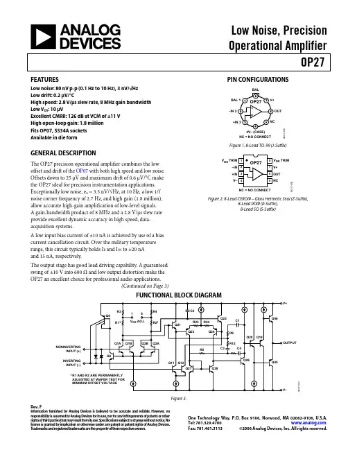
The output stage has good load driving capability. A guaranteed swing of ±10 V into 600 Ω and low output distortion make the OP27 an excellent choice for professional audio applications.
Pin Configurations ........................................................................... 1
Functional Block Diagram .............................................................. 1
GENERAL DESCRIPTION
The OP27 precision operational amplifier combines the low offset and drift of the OP07 with both high speed and low noise. Offsets down to 25 μV and maximum drift of 0.6 μV/°C make the OP27 ideal for precision instrumentation applications. Exceptionally low noise, en = 3.5 nV/√Hz, at 10 Hz, a low 1/f noise corner frequency of 2.7 Hz, and high gain (1.8 million), allow accurate high-gain amplification of low-level signals. A gain-bandwidth product of 8 MHz and a 2.8 V/μs slew rate provide excellent dynamic accuracy in high speed, dataacquisition systems.
Atmel改变命名规则的芯片型号对照表

A t m e l改变命名规则的芯片型号对照表乐享集团公司,写于2021年6月16日ATMLU对应ATMEL芯片:换代选型2011-04-25 23:57AT24C01BN-SH-B/T ATMEL ATMLU701 DIP AT24C01B-PU ATMELATMLU702 DIPATMEL ATMLU703 DIPAT24C02BN-SH-B/T ATMEL ATMLU704 DIP AT24C02B-PU ATMEL ATMLU705 DIPATMEL ATMLU706DIPAT24C04BN-SH-B ATMEL ATMLU707 DIP ATMELATMLU708 DIP ATMEL ATMLU709 DIP ATMEL ATMLU710 DIPATMEL ATMLU711 DIPATMEL ATMLU712 DIPATMEL ATMLU713 DIPATMEL ATMLU714 DIPATMELATMLU715 DIPATMEL ATMLU716 DIPAT24C16BN-SH-B ATMEL ATMLU717 DIPATMEL ATMLU718 DIPATMEL ATMLU719 DIPAT24C256BN-SH-T ATMEL ATMLU720 DIP AT24C256B-PU ATMEL ATMLU721 DIPAT24C256N-10SI18 ATMEL ATMLU722 DIP ATMEL ATMLU723 DIPATMEL ATMLU724 DIPAT24C32CN-SH-T ATMEL ATMLU725DIPATMEL ATMLU726 DIPAT24C512BN-SH25-B ATMEL ATMLU727 DIP AT24C512BN-SH-B ATMELATMLU728 DIPAT24C512B-PU25 ATMELATMLU729 DIPATMEL ATMLU730 DIPATMEL ATMLU731 DIPATMELATMLU732 DIPAT24C64CN-SH-B ATMELATMLU733 DIPAT24C64CN-SH-T ATMEL ATMLU734 DIPATMEL ATMLU735 DIPATMEL ATMLU736 DIPAT25DF041A-SH-B ATMEL ATMLU737DIPATMEL ATMLU738 DIPATMEL ATMLU739DIPAT26DF081A-SSU-SL965 ATMEL ATMLU740 DIP AT26DF081A-SU-SL965 ATMEL ATMLU741 DIP AT26DF161-SUATMEL ATMLU742DIPAT26DF321-SU ATMEL ATMLU743DIPAT27BV256-70JU ATMELATMLU744 DIPAT27C010-70PUATMEL ATMLU745 DIPAT27C040-70PU ATMEL ATMLU746DIPAT27C256R-70PU ATMEL ATMLU748DIP AT27C512R-70JU ATMELATMLU749 DIP AT28BV256-20TU ATMEL ATMLU750 DIP AT28C256-15PU ATMEL ATMLU751 DIP AT28C64B-15JU ATMEL ATMLU752 DIP AT28C64B-15PU ATMEL ATMLU801 DIP AT28C64B-15SUATMELATMLU802 DIPAT29C010A-70JU ATMEL ATMLU803 DIP AT29C020-90JU ATMELATMLU804 DIP AT29C020-90TU ATMEL ATMLU805 DIP AT29C040A-90JU ATMEL ATMLU806 DIP AT29C040A-90TU ATMEL ATMLU807DIP AT29LV020-10TUATMEL ATMLU808 DIP AT29LV040A-15JU ATMEL ATMLU809 DIP AT29LV512-12JUATMELATMLU810 DIP AT45DB021B-SU ATMEL ATMLU811DIP AT45DB041D-SU ATMEL ATMLU812 DIP AT45DB081D-SU ATMELATMLU813 DIP AT45DB161D-SU ATMEL ATMLU814 DIP AT45DB161D-TU ATMEL ATMLU815DIP AT45DB321D-SU ATMEL ATMLU816 DIP AT45DB321D-TU ATMEL ATMLU817 DIPAT47BV163A-70TU ATMEL ATMLU819 DIPAT49BV040B-JU ATMEL ATMLU820 DIPAT49BV322DT-70TU ATMEL ATMLU821 DIP AT49BV512-90TU ATMEL ATMLU822 DIPAT73C213 ATMEL ATMLU823 DIPAT76C112 ATMEL ATMLU824 DIPAT76C120H-MU1-JZ208 ATMEL ATMLU825 DIP AT80251G2D-SLSUM ATMEL ATMLU826 DIP AT80C32X2-3CSUM ATMEL ATMLU827 DIPAT80C32X2-RLTUM ATMEL ATMLU828 DIPAT80C32X2-SLSUM ATMEL ATMLU829 DIPAT83C24-TISIL ATMEL ATMLU830 DIPAT88SC0104C-SU ATMEL ATMLU831 DIPAT88SC153-10SU ATMEL ATMLU832 DIPAT89C2051-12PU ATMEL ATMLU833 DIPAT89C2051-12SU ATMEL ATMLU834 DIPAT89C2051-24PU ATMEL ATMLU835 DIPAT89C2051-24SU ATMEL ATMLU836 DIPAT89C4051-24PU ATMEL ATMLU837 DIPAT89C4051-24SU ATMEL ATMLU838 DIPAT89C5131A-S3SUM ATMEL ATMLU839 DIP AT89C51AC2-RLTUM ATMEL ATMLU840 DIPAT89C51CC01CA-RLTUM ATMEL ATMLU841 DIP AT89C51CC01CA-SLSUM ATMEL ATMLU842 DIP AT89C51CC01UA-RLTUM ATMEL ATMLU843 DIP AT89C51CC01UA-SLSUM ATMEL ATMLU844 DIP AT89C51ED2-RDTUM ATMEL ATMLU845 DIP AT89C51ED2-RLTUM ATMEL ATMLU846 DIP AT89C51ED2-SLSUM ATMEL ATMLU847 DIP AT89C51ED2-SMSUM ATMEL ATMLU848 DIP AT89C51RB2-3CSUM ATMEL ATMLU849 DIP AT89C51RB2-RLTUM ATMEL ATMLU850 DIP AT89C51RB2-SLSUM ATMEL ATMLU851 DIP AT89C51RC2-3CSUM ATMEL ATMLU852 DIP AT89C51RC-24JU ATMEL ATMLU901 DIPAT89C51RC-24PU ATMEL ATMLU902 DIPAT89C51RC2-RLTUM ATMEL ATMLU903 DIP AT89C51RC2-SLSUM ATMEL ATMLU904 DIP AT89C51RD2-RLTUM ATMEL ATMLU905 DIP AT89C51RD2-SLRUM ATMEL ATMLU906 DIP AT89C51RD2-SLSUM ATMEL ATMLU907 DIP AT89C51-24PC ATMEL ATMLU908 DIPAT89C51-24PI ATMEL ATMLU909 DIPAT89C52-24JI ATMEL ATMLU910 DIPAT89C52-24PI ATMEL ATMLH701 SOPAT89C55WD-24AU ATMEL ATMLH702 SOP AT89C55WD-24JU ATMEL ATMLH703 SOP AT89C55WD-24PU ATMEL ATMLH704 SOP AT89LS52-16JU ATMEL ATMLH705 SOPAT89LS52-16PU ATMEL ATMLH706 SOPAT89LV51-12AI ATMEL ATMLH707 SOPAT89S51-24AU ATMEL ATMLH708 SOPAT89S51-24PU ATMEL ATMLH709 SOPAT89S52-24AU ATMEL ATMLH710 SOPAT89S52-24JU ATMEL ATMLH711 SOPAT89S52-24PU ATMEL ATMLH712 SOPAT89S54-3CSIM ATMEL ATMLH713 SOPAT89S54-SLSIM ATMEL ATMLH714 SOPAT89S58-SLSIM ATMEL ATMLH715 SOPAT89S8253-24AU ATMEL ATMLH716 SOP AT89S8253-24JU ATMEL ATMLH717 SOP AT89S8253-24PU ATMEL ATMLH718 SOP AT90CAN128-16AU ATMEL ATMLH719 SOP AT90CAN32-16AU ATMEL ATMLH720 SOP AT91M40800-33AU ATMEL ATMLH721 SOP AT91M55800A-33AU ATMEL ATMLH722 SOP AT91RM9200-CJ-002 ATMEL ATMLH723 SOP AT91RM9200-QU-002 ATMEL ATMLH724 SOPAT91SAM7S256-AU-001 ATMEL ATMLH725 SOP AT91SAM7S321-AU ATMEL ATMLH726 SOPAT91SAM7S32-AU-001 ATMEL ATMLH727 SOP AT91SAM7S64-AU-001 ATMEL ATMLH728 SOP AT91SAM7SE32-AU ATMEL ATMLH729 SOPAT91SAM7X256-AU ATMEL ATMLH730 SOPAT91SAM9260-CJ ATMEL ATMLH731 SOPAT91SAM9260-EK ATMEL ATMLH732 SOPAT91SAM9261-EK ATMEL ATMLH733 SOPAT91SAM9261S-CU ATMEL ATMLH734 SOPAT91SAM9263-CU ATMEL ATMLH735 SOPAT91SAM7X-EK ATMEL ATMLH736 SOPAT91SAM-ICE ATMEL ATMLH737 SOPATMEL ATMLH738 SOPATMEL ATMLH739 SOPAT93C46DN-SH-B ATMEL ATMLH740 SOPAT93C46D-TH-T ATMEL ATMLH741 SOPATMEL ATMLH742 SOPATMEL ATMLH743 SOPAT93C66A-10PU27 ATMEL ATMLH744 SOPATMEL ATMLH745 SOPATMEL ATMLH746 SOPATAVRDRAGON ATMEL ATMLH747 SOPATAVRISP2 ATMEL ATMLH748 SOPATF1502AS-15JC44 ATMEL ATMLH749 SOP ATF1508AS-15AC100 ATMEL ATMLH750 SOP ATF1508AS-15JC84 ATMEL ATMLH751 SOP ATF16V8B-15JU ATMEL ATMLH752 SOP ATF16V8B-15PC ATMEL ATMLH801 SOP ATF16V8B-15PU ATMEL ATMLH802 SOP ATF16V8BQL-15JC ATMEL ATMLH803 SOP ATF20V8B-15JC ATMEL ATMLH804 SOP ATJTAGICE2 ATMEL ATMLH805 SOP ATMEGA1280V-8AU ATMEL ATMLH806 SOP ATMEGA128-16AU ATMEL ATMLH807 SOP ATMEGA128L-8AU ATMEL ATMLH808 SOP ATMEGA16-16AU ATMEL ATMLH809 SOP ATMEGA16-16PU ATMEL ATMLH810 SOP ATMEGA162-16PU ATMEL ATMLH811 SOP ATMEGA162V-8AU ATMEL ATMLH812 SOP ATMEGA168-20AU ATMEL ATMLH813 SOP ATMEGA168-20MU ATMEL ATMLH814 SOP ATMEGA168-20PU ATMEL ATMLH815 SOP ATMEGA168V-10AU ATMEL ATMLH816 SOP ATMEGA169P-16AU ATMEL ATMLH817 SOP ATMEGA169PV-8AU ATMEL ATMLH818 SOPATMEGA169V-8AU ATMEL ATMLH819 SOP ATMEGA16L-8AU ATMEL ATMLH820 SOP ATMEGA16L-8PU ATMEL ATMLH821 SOP ATMEGA32-16AU ATMEL ATMLH822 SOP ATMEGA32-16PU ATMEL ATMLH823 SOP ATMEGA325V-8MU ATMEL ATMLH824 SOP ATMEGA32L-8AU ATMEL ATMLH825 SOP ATMEGA32L-8PU ATMEL ATMLH826 SOP ATMEGA48-20AU ATMEL ATMLH827 SOP ATMEGA48V-10AU ATMEL ATMLH828 SOP ATMEGA48V-10PU ATMEL ATMLH829 SOP ATMEGA48V-10MU ATMEL ATMLH830 SOP ATMEGA640V-8AU ATMEL ATMLH831 SOP ATMEGA64-16AU ATMEL ATMLH832 SOP ATMEGA64L-8AU ATMEL ATMLH833 SOP ATMEGA8-16AU ATMEL ATMLH834 SOP ATMEGA8-16PU ATMEL ATMLH835 SOP ATMEGA8515-16AU ATMEL ATMLH836 SOP ATMEGA8515-16JU ATMEL ATMLH837 SOP ATMEGA8515-16PU ATMEL ATMLH838 SOP ATMEGA8515L-8JU ATMEL ATMLH839 SOP ATMEGA8535-16JI ATMEL ATMLH840 SOP ATMEGA8535-16JU ATMEL ATMLH841 SOPATMEGA8535-16PU ATMEL ATMLH842 SOP ATMEGA8535L-8AU ATMEL ATMLH843 SOP ATMEGA8535L-8JU ATMEL ATMLH844 SOP ATMEGA8535L-8PU ATMEL ATMLH845 SOP ATMEGA88-20AU ATMEL ATMLH846 SOP ATMEGA88-20MU ATMEL ATMLH847 SOP ATMEGA88-20PU ATMEL ATMLH848 SOP ATMEGA88V-10AU ATMEL ATMLH849 SOP ATMEGA88V-10MU ATMEL ATMLH850 SOP ATMEGA88V-10PU ATMEL ATMLH851 SOP ATMEGA8L-8AU ATMEL ATMLH852 SOP ATMEGA8L-8PU ATMEL ATMLH901 SOP ATTINY11L-2SU ATMEL ATMLH902 SOP ATTINY13-20SU ATMEL ATMLH903 SOP ATTINY13V-10PU ATMEL ATMLH904 SOP ATTINY13V-10SSU ATMEL ATMLH905 SOP ATTINY13V-10SU ATMEL ATMLH906 SOP ATTINY15L-1PU ATMEL ATMLH907 SOP ATTINY2313-20PU ATMEL ATMLH908 SOP ATTINY2313-20SU ATMEL ATMLH909 SOP ATTINY2313V-10PU ATMEL ATMLH910 SOP AT24C01BN-SH-B/T ATMEL ATMLU701 DIP AT24C01B-PI ATMEL ATMLU702 DIPAT24C02BN-SH-B/T ATMEL ATMLU704 DIP AT24C02B-PI ATMEL ATMLU705 DIPATMEL ATMLU706 DIPAT24C04BN-SH-B ATMEL ATMLU707 DIP ATMEL ATMLU708 DIPATMEL ATMLU709 DIPATMEL ATMLU710 DIPATMEL ATMLU711 DIPATMEL ATMLU712 DIPATMEL ATMLU713 DIPATMEL ATMLU714 DIPATMEL ATMLU715 DIPATMEL ATMLU716 DIPAT24C16BN-SH-B ATMEL ATMLU717 DIP ATMEL ATMLU718 DIPATMEL ATMLU719 DIPAT24C256BN-SH-T ATMEL ATMLU720 DIP AT24C256B-PI ATMEL ATMLU721 DIPAT24C256N-10SI18 ATMEL ATMLU722 DIP ATMEL ATMLU723 DIPATMEL ATMLU724 DIPAT24C32CN-SH-T ATMEL ATMLU725 DIPAT24C512BN-SH25-B ATMEL ATMLU727 DIP AT24C512BN-SH-B ATMEL ATMLU728 DIPAT24C512B-PI25 ATMEL ATMLU729 DIPATMEL ATMLU730 DIPATMEL ATMLU731 DIPATMEL ATMLU732 DIPAT24C64CN-SH-B ATMEL ATMLU733 DIPAT24C64CN-SH-T ATMEL ATMLU734 DIPATMEL ATMLU735 DIPATMEL ATMLU736 DIPAT25DF041A-SH-B ATMEL ATMLU737 DIPATMEL ATMLU738 DIPATMEL ATMLU739 DIPAT26DF081A-SSI-SL965 ATMEL ATMLU740 DIP AT26DF081A-SI-SL965 ATMEL ATMLU741 DIP AT26DF161-SI ATMEL ATMLU742 DIPAT26DF321-SI ATMEL ATMLU743 DIPAT27BV256-70JI ATMEL ATMLU744 DIPAT27C010-70PI ATMEL ATMLU745 DIPAT27C040-70PI ATMEL ATMLU746 DIPAT27C256R-70JI ATMEL ATMLU747 DIPAT27C256R-70PI ATMEL ATMLU748 DIPAT28BV256-20TI ATMEL ATMLU750 DIP AT28C256-15PI ATMEL ATMLU751 DIP AT28C64B-15JI ATMEL ATMLU752 DIP AT28C64B-15PI ATMEL ATMLU801 DIP AT28C64B-15SI ATMEL ATMLU802 DIP AT29C010A-70JI ATMEL ATMLU803 DIP AT29C020-90JI ATMEL ATMLU804 DIP AT29C020-90TI ATMEL ATMLU805 DIP AT29C040A-90JI ATMEL ATMLU806 DIP AT29C040A-90TI ATMEL ATMLU807 DIP AT29LV020-10TI ATMEL ATMLU808 DIP AT29LV040A-15JI ATMEL ATMLU809 DIP AT29LV512-12JI ATMEL ATMLU810 DIP AT45DB021B-SI ATMEL ATMLU811 DIP AT45DB041D-SI ATMEL ATMLU812 DIP AT45DB081D-SI ATMEL ATMLU813 DIP AT45DB161D-SI ATMEL ATMLU814 DIP AT45DB161D-TI ATMEL ATMLU815 DIP AT45DB321D-SI ATMEL ATMLU816 DIP AT45DB321D-TI ATMEL ATMLU817 DIP AT45DB642D-TI ATMEL ATMLU818 DIP AT47BV163A-70TI ATMEL ATMLU819 DIPAT49BV322DT-70TI ATMEL ATMLU821 DIP AT49BV512-90TI ATMEL ATMLU822 DIPAT73C213 ATMEL ATMLU823 DIPAT76C112 ATMEL ATMLU824 DIPAT76C120H-MI1-JZ208 ATMEL ATMLU825 DIP AT80251G2D-SLSIM ATMEL ATMLU826 DIP AT80C32X2-3CSIM ATMEL ATMLU827 DIPAT80C32X2-RLTIM ATMEL ATMLU828 DIPAT80C32X2-SLSIM ATMEL ATMLU829 DIPAT83C24-TISIL ATMEL ATMLU830 DIPAT88SC0104C-SI ATMEL ATMLU831 DIPAT88SC153-10SI ATMEL ATMLU832 DIPAT89C2051-12PI ATMEL ATMLU833 DIPAT89C2051-12SI ATMEL ATMLU834 DIPAT89C2051-24PI ATMEL ATMLU835 DIPAT89C2051-24SI ATMEL ATMLU836 DIPAT89C4051-24PI ATMEL ATMLU837 DIPAT89C4051-24SI ATMEL ATMLU838 DIPAT89C5131A-S3SIM ATMEL ATMLU839 DIP AT89C51AC2-RLTIM ATMEL ATMLU840 DIP AT89C51CC01CA-RLTIM ATMEL ATMLU841 DIP AT89C51CC01CA-SLSIM ATMEL ATMLU842 DIPAT89C51CC01IA-RLTIM ATMEL ATMLU843 DIP AT89C51CC01IA-SLSIM ATMEL ATMLU844 DIP AT89C51ED2-RDTIM ATMEL ATMLU845 DIP AT89C51ED2-RLTIM ATMEL ATMLU846 DIP AT89C51ED2-SLSIM ATMEL ATMLU847 DIP AT89C51ED2-SMSIM ATMEL ATMLU848 DIP AT89C51RB2-3CSIM ATMEL ATMLU849 DIP AT89C51RB2-RLTIM ATMEL ATMLU850 DIP AT89C51RB2-SLSIM ATMEL ATMLU851 DIP AT89C51RC2-3CSIM ATMEL ATMLU852 DIP AT89C51RC-24JI ATMEL ATMLU901 DIPAT89C51RC-24PI ATMEL ATMLU902 DIPAT89C51RC2-RLTIM ATMEL ATMLU903 DIP AT89C51RC2-SLSIM ATMEL ATMLU904 DIP AT89C51RD2-RLTIM ATMEL ATMLU905 DIP AT89C51RD2-SLRIM ATMEL ATMLU906 DIP AT89C51RD2-SLSIM ATMEL ATMLU907 DIP AT89C51-24PC ATMEL ATMLU908 DIPAT89C51-24PI ATMEL ATMLU909 DIPAT89C52-24JI ATMEL ATMLU910 DIPAT89C52-24PI ATMEL ATMLH701 SOPAT89C55WD-24AI ATMEL ATMLH702 SOPAT89C55WD-24JI ATMEL ATMLH703 SOPAT89C55WD-24PI ATMEL ATMLH704 SOPAT89LS52-16JI ATMEL ATMLH705 SOPAT89LS52-16PI ATMEL ATMLH706 SOPAT89LV51-12AI ATMEL ATMLH707 SOPAT89S51-24AI ATMEL ATMLH708 SOPAT89S51-24PI ATMEL ATMLH709 SOPAT89S52-24AI ATMEL ATMLH710 SOPAT89S52-24JI ATMEL ATMLH711 SOPAT89S52-24PI ATMEL ATMLH712 SOPAT89S54-3CSIM ATMEL ATMLH713 SOPAT89S54-SLSIM ATMEL ATMLH714 SOPAT89S58-SLSIM ATMEL ATMLH715 SOPAT89S8253-24AI ATMEL ATMLH716 SOPAT89S8253-24JI ATMEL ATMLH717 SOPAT89S8253-24PI ATMEL ATMLH718 SOPAT90CAN128-16AI ATMEL ATMLH719 SOPAT90CAN32-16AI ATMEL ATMLH720 SOPAT91M40800-33AI ATMEL ATMLH721 SOPAT91M55800A-33AI ATMEL ATMLH722 SOP AT91RM9200-CJ-002 ATMEL ATMLH723 SOP AT91RM9200-QI-002 ATMEL ATMLH724 SOP AT91SAM7S256-AI-001 ATMEL ATMLH725 SOP AT91SAM7S321-AI ATMEL ATMLH726 SOPAT91SAM7S64-AI-001 ATMEL ATMLH728 SOP AT91SAM7SE32-AI ATMEL ATMLH729 SOP AT91SAM7X256-AI ATMEL ATMLH730 SOP AT91SAM9260-CJ ATMEL ATMLH731 SOPAT91SAM9260-EK ATMEL ATMLH732 SOPAT91SAM9261-EK ATMEL ATMLH733 SOPAT91SAM9261S-CI ATMEL ATMLH734 SOP AT91SAM9263-CI ATMEL ATMLH735 SOPAT91SAM7X-EK ATMEL ATMLH736 SOPAT91SAM-ICE ATMEL ATMLH737 SOPATMEL ATMLH738 SOPATMEL ATMLH739 SOPAT93C46DN-SH-B ATMEL ATMLH740 SOPAT93C46D-TH-T ATMEL ATMLH741 SOPATMEL ATMLH742 SOPATMEL ATMLH743 SOPAT93C66A-10PI27 ATMEL ATMLH744 SOPATMEL ATMLH745 SOPATMEL ATMLH746 SOPATAVRDRAGON ATMEL ATMLH747 SOP ATAVRISP2 ATMEL ATMLH748 SOPATF1502AS-15JC44 ATMEL ATMLH749 SOPATF1508AS-15JC84 ATMEL ATMLH751 SOP ATF16V8B-15JI ATMEL ATMLH752 SOP ATF16V8B-15PC ATMEL ATMLH801 SOP ATF16V8B-15PI ATMEL ATMLH802 SOP ATF16V8BQL-15JC ATMEL ATMLH803 SOP ATF20V8B-15JC ATMEL ATMLH804 SOP AT JTAGICE MKII ATMEL ATMLH805 SOP ATMEGA1280V-8AI ATMEL ATMLH806 SOP ATMEGA128-16AI ATMEL ATMLH807 SOP ATMEGA128L-8AI ATMEL ATMLH808 SOP ATMEGA16-16AI ATMEL ATMLH809 SOP ATMEGA16-16PI ATMEL ATMLH810 SOP ATMEGA162-16PI ATMEL ATMLH811 SOP ATMEGA162V-8AI ATMEL ATMLH812 SOP ATMEGA168-20AI ATMEL ATMLH813 SOP ATMEGA168-20MI ATMEL ATMLH814 SOP ATMEGA168-20PI ATMEL ATMLH815 SOP ATMEGA168V-10AI ATMEL ATMLH816 SOP ATMEGA169P-16AI ATMEL ATMLH817 SOP ATMEGA169PV-8AI ATMEL ATMLH818 SOP ATMEGA169V-8AI ATMEL ATMLH819 SOP ATMEGA16L-8AI ATMEL ATMLH820 SOPATMEGA16L-8PI ATMEL ATMLH821 SOP ATMEGA32-16AI ATMEL ATMLH822 SOP ATMEGA32-16PI ATMEL ATMLH823 SOP ATMEGA325V-8MI ATMEL ATMLH824 SOP ATMEGA32L-8AI ATMEL ATMLH825 SOP ATMEGA32L-8PI ATMEL ATMLH826 SOP ATMEGA48-20AI ATMEL ATMLH827 SOP ATMEGA48V-10AI ATMEL ATMLH828 SOP ATMEGA48V-10PI ATMEL ATMLH829 SOP ATMEGA48V-10MI ATMEL ATMLH830 SOP ATMEGA640V-8AI ATMEL ATMLH831 SOP ATMEGA64-16AI ATMEL ATMLH832 SOP ATMEGA64L-8AI ATMEL ATMLH833 SOP ATMEGA8-16AI ATMEL ATMLH834 SOP ATMEGA8-16PI ATMEL ATMLH835 SOP ATMEGA8515-16AI ATMEL ATMLH836 SOP ATMEGA8515-16JI ATMEL ATMLH837 SOP ATMEGA8515-16PI ATMEL ATMLH838 SOP ATMEGA8515L-8JI ATMEL ATMLH839 SOP ATMEGA8535-16JI ATMEL ATMLH840 SOP ATMEGA8535-16JI ATMEL ATMLH841 SOP ATMEGA8535-16PI ATMEL ATMLH842 SOP ATMEGA8535L-8AI ATMEL ATMLH843 SOPATMEGA8535L-8JI ATMEL ATMLH844 SOP ATMEGA8535L-8PI ATMEL ATMLH845 SOP ATMEGA88-20AI ATMEL ATMLH846 SOP ATMEGA88-20MI ATMEL ATMLH847 SOP ATMEGA88-20PI ATMEL ATMLH848 SOP ATMEGA88V-10AI ATMEL ATMLH849 SOP ATMEGA88V-10MI ATMEL ATMLH850 SOP ATMEGA88V-10PI ATMEL ATMLH851 SOP ATMEGA8L-8AI ATMEL ATMLH852 SOP ATMEGA8L-8PI ATMEL ATMLH901 SOP ATTINY11L-2SI ATMEL ATMLH902 SOP ATTINY13-20SI ATMEL ATMLH903 SOP ATTINY13V-10PI ATMEL ATMLH904 SOP ATTINY13V-10SSI ATMEL ATMLH905 SOP ATTINY13V-10SI ATMEL ATMLH906 SOP ATTINY15L-1PI ATMEL ATMLH907 SOP ATTINY2313-20PI ATMEL ATMLH908 SOP ATTINY2313-20SI ATMEL ATMLH909 SOP ATTINY2313V-10PI ATMEL ATMLH910 SOP AT17LV010-10PI 1000 ATMEL0007AT17LV256-10JI 1000 ATMEL0008AT17LV256-10PC 1000 ATMEL0009AT17LV256-10PI 1000 ATMEL0010AT17LV512-10PC 1000 ATMEL0011 AT17LV512-10PC 1000 ATMEL0012 AT17LV512A-10PI 1000 ATMEL0013 AT17LV65-10PI 1000 ATMEL0014 AT22V10-15DC 1000 ATMEL0015 AT22V10-15JC 1000 ATMEL0016 AT22V10-15KC 1000 ATMEL0017 AT22V10-20DC 1000 ATMEL0018 AT22V10-20JC 1000 ATMEL0019 AT22V10-25DC 1000 ATMEL0020 AT22V10-25JC 1000 ATMEL0021 AT22V10-25JI 1000 ATMEL0022 AT22V10-25KC 1000 ATMEL0023 AT22V10-35DC 1000 ATMEL0024 AT22V10-35JC 1000 ATMEL0025 AT22V10-35KC 1000 ATMEL0026 AT22V10-35PC 1000 ATMEL0027 AT22V10L-20PC 1000 ATMEL0028 AT22V10L-25DC 1000 ATMEL0029 AT22V10L-25JC 1000 ATMEL0030 AT22V10L-25JI 1000 ATMEL0031 AT22V10L-35DC 1000 ATMEL0032 AT24C01-10PC 1000 ATMEL0033AT24C01-10PI 1000 ATMEL00351000 ATMEL0036AT24C01-10SC 1000 ATMEL0037 AT24C01A-10PC 8000 ATMEL0038 AT24C01A-10SC 8000 ATMEL0039 8000 ATMEL00408000 ATMEL06018000 ATMEL0041AT24C01BN-SH-B 8000 ATMEL0042 AT24C01BN-SH-T 8000 ATMEL0043 AT24C01B-PU 8000 ATMEL0602AT24C01B-TH-B 8000 ATMEL0044 AT24C01B-TH-T 8000 ATMEL0045 AT24C01BTSU-T 8000 ATMEL0603 AT24C01BU3-UU-T 8000 ATMEL0604 AT24C01B-W-11 8000 ATMEL0046 AT24C01BY6-YH-T 8000 ATMEL0047 8000 ATMEL0048AT24C02-10PC 8000 ATMEL00498000 ATMEL00508000 ATMEL00518000 ATMEL00528000 ATMEL01018000 ATMEL01028000 ATMEL01038000 ATMEL06068000 ATMEL01048000 ATMEL06078000 ATMEL01058000 ATMEL01068000 ATMEL01078000 ATMEL01088000 ATMEL01098000 ATMEL06088000 ATMEL01108000 ATMEL01118000 ATMEL0112 8000 ATMEL0113 8000 ATMEL01148000 ATMEL06098000 ATMEL06108000 ATMEL01158000 ATMEL01168000 ATMEL01178000 ATMEL06118000 ATMEL06138000 ATMEL01188000 ATMEL01198000 ATMEL01208000 ATMEL06148000 ATMEL06158000 ATMEL01218000 ATMEL01228000 ATMEL01238000 ATMEL06168000 ATMEL06178000 ATMEL01248000 ATMEL0125AT24C16-10PI 8000 ATMEL0126 8000 ATMEL0127AT24C164-10PC 8000 ATMEL0128 8000 ATMEL0129AT24C164-10PI 8000 ATMEL0130 AT24C164-10SC 8000 ATMEL0131 8000 ATMEL01328000 ATMEL01338000 ATMEL01348000 ATMEL01368000 ATMEL01378000 ATMEL0138AT24C16N-SC 8000 ATMEL0139 8000 ATMEL01408000 ATMEL01418000 ATMEL01428000 ATMEL01438000 ATMEL01448000 ATMEL01458000 ATMEL0146AT24C256-10PC 8000 ATMEL0147 8000 ATMEL01488000 ATMEL01498000 ATMEL01508000 ATMEL01518000 ATMEL01528000 ATMEL0201AT24C32-10PC 8000 ATMEL0202 AT24C32- 8000 ATMEL02038000 ATMEL02048000 ATMEL02058000 ATMEL0207AT24C32N-SC 8000 ATMEL0208AT24C32W-10SI 8000 ATMEL02098000 ATMEL02108000 ATMEL06188000 ATMEL02118000 ATMEL02128000 ATMEL02138000 ATMEL02148000 ATMEL06198000 ATMEL02158000 ATMEL02168000 ATMEL02178000 ATMEL02188000 ATMEL02198000 ATMEL06208000 ATMEL02208000 ATMEL0221AT24C64-SC 8000 ATMEL0222AT24RF08CN 1000 ATMEL0223。
Atmel芯片新命名型对照表
AT24C01BN-SH-B/T ATMEL ATMLU701DIP AT24C01B-PU ATMEL ATMLU702DIP AT24C02B-10PU-1.8ATMEL ATMLU703DIP AT24C02BN-SH-B/T ATMEL ATMLU704DIP AT24C02B-PU ATMEL ATMLU705DIP AT24C04-10PU-2.7ATMEL ATMLU706DIP AT24C04BN-SH-B ATMEL ATMLU707DIP AT24C04N-10SU-2.7ATMEL ATMLU708DIP AT24C08A-10PU-2.7ATMEL ATMLU709DIP AT24C08A-10TU-2.7ATMEL ATMLU710DIP AT24C08AN-10SU-2.7ATMEL ATMLU711DIP AT24C128-10PU-2.7ATMEL ATMLU712DIP AT24C128N-10SU-2.7-SL383ATMEL ATMLU713DIP AT24C16A-10PU-2.7ATMEL ATMLU714DIP AT24C16A-10TI-1.8ATMEL ATMLU715DIP AT24C16AN-10SU-2.7ATMEL ATMLU716DIP AT24C16BN-SH-B ATMEL ATMLU717DIP AT24C256B-10PU-1.8ATMEL ATMLU718DIP AT24C256BN-10SU-1.8ATMEL ATMLU719DIP AT24C256BN-SH-T ATMEL ATMLU720DIP AT24C256B-PU ATMEL ATMLU721DIP AT24C256N-10SI18ATMEL ATMLU722DIP AT24C32A-10PU-2.7ATMEL ATMLU723DIP AT24C32AN-10SU-2.7ATMEL ATMLU724DIP AT24C32CN-SH-T ATMEL ATMLU725DIP AT24C512-10PU-2.7ATMEL ATMLU726DIP AT24C512BN-SH25-B ATMEL ATMLU727DIP AT24C512BN-SH-B ATMEL ATMLU728DIP AT24C512B-PU25ATMEL ATMLU729DIP AT24C512N-10SU-2.7ATMEL ATMLU730DIP AT24C64A-10PU-2.7ATMEL ATMLU731DIP AT24C64AN-10SU-2.7ATMEL ATMLU732DIP AT24C64CN-SH-B ATMEL ATMLU733DIP AT24C64CN-SH-T ATMEL ATMLU734DIP AT25128A-10PU-2.7ATMEL ATMLU735DIP AT25256AN-10SU-2.7ATMEL ATMLU736DIP AT25DF041A-SH-B ATMEL ATMLU737DIP AT25F1024AN-10SU-2.7-SL383ATMEL ATMLU738DIP AT25F512AN-10SU-2.7-SL383ATMEL ATMLU739DIP AT26DF081A-SSU-SL965ATMEL ATMLU740DIP AT26DF081A-SU-SL965ATMEL ATMLU741DIP AT26DF161-SU ATMEL ATMLU742DIP AT26DF321-SU ATMEL ATMLU743DIP AT27BV256-70JU ATMEL ATMLU744DIP AT27C010-70PU ATMEL ATMLU745DIP AT27C040-70PU ATMEL ATMLU746DIP AT27C256R-70JU ATMEL ATMLU747DIPAT27C256R-70PU ATMEL ATMLU748DIP AT27C512R-70JU ATMEL ATMLU749DIP AT28BV256-20TU ATMEL ATMLU750DIP AT28C256-15PU ATMEL ATMLU751DIP AT28C64B-15JU ATMEL ATMLU752DIP AT28C64B-15PU ATMEL ATMLU801DIP AT28C64B-15SU ATMEL ATMLU802DIP AT29C010A-70JU ATMEL ATMLU803DIP AT29C020-90JU ATMEL ATMLU804DIP AT29C020-90TU ATMEL ATMLU805DIP AT29C040A-90JU ATMEL ATMLU806DIP AT29C040A-90TU ATMEL ATMLU807DIP AT29LV020-10TU ATMEL ATMLU808DIP AT29LV040A-15JU ATMEL ATMLU809DIP AT29LV512-12JU ATMEL ATMLU810DIP AT45DB021B-SU ATMEL ATMLU811DIP AT45DB041D-SU ATMEL ATMLU812DIP AT45DB081D-SU ATMEL ATMLU813DIP AT45DB161D-SU ATMEL ATMLU814DIP AT45DB161D-TU ATMEL ATMLU815DIP AT45DB321D-SU ATMEL ATMLU816DIP AT45DB321D-TU ATMEL ATMLU817DIP AT45DB642D-TU ATMEL ATMLU818DIP AT47BV163A-70TU ATMEL ATMLU819DIP AT49BV040B-JU ATMEL ATMLU820DIP AT49BV322DT-70TU ATMEL ATMLU821DIP AT49BV512-90TU ATMEL ATMLU822DIP AT73C213ATMEL ATMLU823DIP AT76C112ATMEL ATMLU824DIP AT76C120H-MU1-JZ208ATMEL ATMLU825DIP AT80251G2D-SLSUM ATMEL ATMLU826DIP AT80C32X2-3CSUM ATMEL ATMLU827DIP AT80C32X2-RLTUM ATMEL ATMLU828DIP AT80C32X2-SLSUM ATMEL ATMLU829DIP AT83C24-TISIL ATMEL ATMLU830DIP AT88SC0104C-SU ATMEL ATMLU831DIP AT88SC153-10SU ATMEL ATMLU832DIP AT89C2051-12PU ATMEL ATMLU833DIP AT89C2051-12SU ATMEL ATMLU834DIP AT89C2051-24PU ATMEL ATMLU835DIP AT89C2051-24SU ATMEL ATMLU836DIP AT89C4051-24PU ATMEL ATMLU837DIP AT89C4051-24SU ATMEL ATMLU838DIP AT89C5131A-S3SUM ATMEL ATMLU839DIP AT89C51AC2-RLTUM ATMEL ATMLU840DIP AT89C51CC01CA-RLTUM ATMEL ATMLU841DIP AT89C51CC01CA-SLSUM ATMEL ATMLU842DIPAT89C51CC01UA-RLTUM ATMEL ATMLU843DIP AT89C51CC01UA-SLSUM ATMEL ATMLU844DIP AT89C51ED2-RDTUM ATMEL ATMLU845DIP AT89C51ED2-RLTUM ATMEL ATMLU846DIP AT89C51ED2-SLSUM ATMEL ATMLU847DIP AT89C51ED2-SMSUM ATMEL ATMLU848DIP AT89C51RB2-3CSUM ATMEL ATMLU849DIP AT89C51RB2-RLTUM ATMEL ATMLU850DIP AT89C51RB2-SLSUM ATMEL ATMLU851DIP AT89C51RC2-3CSUM ATMEL ATMLU852DIP AT89C51RC-24JU ATMEL ATMLU901DIP AT89C51RC-24PU ATMEL ATMLU902DIP AT89C51RC2-RLTUM ATMEL ATMLU903DIP AT89C51RC2-SLSUM ATMEL ATMLU904DIP AT89C51RD2-RLTUM ATMEL ATMLU905DIP AT89C51RD2-SLRUM ATMEL ATMLU906DIP AT89C51RD2-SLSUM ATMEL ATMLU907DIP AT89C51-24PC ATMEL ATMLU908DIP AT89C51-24PI ATMEL ATMLU909DIP AT89C52-24JI ATMEL ATMLU910DIP AT89C52-24PI ATMEL ATMLH701SOP AT89C55WD-24AU ATMEL ATMLH702SOP AT89C55WD-24JU ATMEL ATMLH703SOP AT89C55WD-24PU ATMEL ATMLH704SOP AT89LS52-16JU ATMEL ATMLH705SOP AT89LS52-16PU ATMEL ATMLH706SOP AT89LV51-12AI ATMEL ATMLH707SOP AT89S51-24AU ATMEL ATMLH708SOP AT89S51-24PU ATMEL ATMLH709SOP AT89S52-24AU ATMEL ATMLH710SOP AT89S52-24JU ATMEL ATMLH711SOP AT89S52-24PU ATMEL ATMLH712SOP AT89S54-3CSIM ATMEL ATMLH713SOP AT89S54-SLSIM ATMEL ATMLH714SOP AT89S58-SLSIM ATMEL ATMLH715SOP AT89S8253-24AU ATMEL ATMLH716SOP AT89S8253-24JU ATMEL ATMLH717SOP AT89S8253-24PU ATMEL ATMLH718SOP AT90CAN128-16AU ATMEL ATMLH719SOP AT90CAN32-16AU ATMEL ATMLH720SOP AT91M40800-33AU ATMEL ATMLH721SOP AT91M55800A-33AU ATMEL ATMLH722SOP AT91RM9200-CJ-002ATMEL ATMLH723SOP AT91RM9200-QU-002ATMEL ATMLH724SOP AT91SAM7S256-AU-001ATMEL ATMLH725SOP AT91SAM7S321-AU ATMEL ATMLH726SOP AT91SAM7S32-AU-001ATMEL ATMLH727SOPAT91SAM7S64-AU-001ATMEL ATMLH728SOP AT91SAM7SE32-AU ATMEL ATMLH729SOP AT91SAM7X256-AU ATMEL ATMLH730SOP AT91SAM9260-CJ ATMEL ATMLH731SOP AT91SAM9260-EK ATMEL ATMLH732SOP AT91SAM9261-EK ATMEL ATMLH733SOP AT91SAM9261S-CU ATMEL ATMLH734SOP AT91SAM9263-CU ATMEL ATMLH735SOP AT91SAM7X-EK ATMEL ATMLH736SOP AT91SAM-ICE ATMEL ATMLH737SOP AT93C46-10PU-2.7ATMEL ATMLH738SOP AT93C46-10SU-2.7ATMEL ATMLH739SOP AT93C46DN-SH-B ATMEL ATMLH740SOP AT93C46D-TH-T ATMEL ATMLH741SOP AT93C56A-10PU-2.7ATMEL ATMLH742SOP AT93C56A-10SU-2.7ATMEL ATMLH743SOP AT93C66A-10PU27ATMEL ATMLH744SOP AT93C66A-10SU-2.7ATMEL ATMLH745SOP AT93C66A-10SU-2.7-SL383ATMEL ATMLH746SOP ATAVRDRAGON ATMEL ATMLH747SOP ATAVRISP2ATMEL ATMLH748SOP ATF1502AS-15JC44ATMEL ATMLH749SOP ATF1508AS-15AC100ATMEL ATMLH750SOP ATF1508AS-15JC84ATMEL ATMLH751SOP ATF16V8B-15JU ATMEL ATMLH752SOP ATF16V8B-15PC ATMEL ATMLH801SOP ATF16V8B-15PU ATMEL ATMLH802SOP ATF16V8BQL-15JC ATMEL ATMLH803SOP ATF20V8B-15JC ATMEL ATMLH804SOP ATJTAGICE2ATMEL ATMLH805SOP ATMEGA1280V-8AU ATMEL ATMLH806SOP ATMEGA128-16AU ATMEL ATMLH807SOP ATMEGA128L-8AU ATMEL ATMLH808SOP ATMEGA16-16AU ATMEL ATMLH809SOP ATMEGA16-16PU ATMEL ATMLH810SOP ATMEGA162-16PU ATMEL ATMLH811SOP ATMEGA162V-8AU ATMEL ATMLH812SOP ATMEGA168-20AU ATMEL ATMLH813SOP ATMEGA168-20MU ATMEL ATMLH814SOP ATMEGA168-20PU ATMEL ATMLH815SOP ATMEGA168V-10AU ATMEL ATMLH816SOP ATMEGA169P-16AU ATMEL ATMLH817SOP ATMEGA169PV-8AU ATMEL ATMLH818SOP ATMEGA169V-8AU ATMEL ATMLH819SOP ATMEGA16L-8AU ATMEL ATMLH820SOP ATMEGA16L-8PU ATMEL ATMLH821SOP ATMEGA32-16AU ATMEL ATMLH822SOPATMEGA32-16PU ATMEL ATMLH823SOP ATMEGA325V-8MU ATMEL ATMLH824SOP ATMEGA32L-8AU ATMEL ATMLH825SOP ATMEGA32L-8PU ATMEL ATMLH826SOP ATMEGA48-20AU ATMEL ATMLH827SOP ATMEGA48V-10AU ATMEL ATMLH828SOP ATMEGA48V-10PU ATMEL ATMLH829SOP ATMEGA48V-10MU ATMEL ATMLH830SOP ATMEGA640V-8AU ATMEL ATMLH831SOP ATMEGA64-16AU ATMEL ATMLH832SOP ATMEGA64L-8AU ATMEL ATMLH833SOP ATMEGA8-16AU ATMEL ATMLH834SOP ATMEGA8-16PU ATMEL ATMLH835SOP ATMEGA8515-16AU ATMEL ATMLH836SOP ATMEGA8515-16JU ATMEL ATMLH837SOP ATMEGA8515-16PU ATMEL ATMLH838SOP ATMEGA8515L-8JU ATMEL ATMLH839SOP ATMEGA8535-16JI ATMEL ATMLH840SOP ATMEGA8535-16JU ATMEL ATMLH841SOP ATMEGA8535-16PU ATMEL ATMLH842SOP ATMEGA8535L-8AU ATMEL ATMLH843SOP ATMEGA8535L-8JU ATMEL ATMLH844SOP ATMEGA8535L-8PU ATMEL ATMLH845SOP ATMEGA88-20AU ATMEL ATMLH846SOP ATMEGA88-20MU ATMEL ATMLH847SOP ATMEGA88-20PU ATMEL ATMLH848SOP ATMEGA88V-10AU ATMEL ATMLH849SOP ATMEGA88V-10MU ATMEL ATMLH850SOP ATMEGA88V-10PU ATMEL ATMLH851SOP ATMEGA8L-8AU ATMEL ATMLH852SOP ATMEGA8L-8PU ATMEL ATMLH901SOP ATTINY11L-2SU ATMEL ATMLH902SOP ATTINY13-20SU ATMEL ATMLH903SOP ATTINY13V-10PU ATMEL ATMLH904SOP ATTINY13V-10SSU ATMEL ATMLH905SOP ATTINY13V-10SU ATMEL ATMLH906SOP ATTINY15L-1PU ATMEL ATMLH907SOP ATTINY2313-20PU ATMEL ATMLH908SOP ATTINY2313-20SU ATMEL ATMLH909SOP ATTINY2313V-10PU ATMEL ATMLH910SOP AT24C01BN-SH-B/T ATMEL ATMLU701DIP AT24C01B-PI ATMEL ATMLU702DIP AT24C02B-10PI-1.8ATMEL ATMLU703DIP AT24C02BN-SH-B/T ATMEL ATMLU704DIP AT24C02B-PI ATMEL ATMLU705DIP AT24C04-10PI-2.7ATMEL ATMLU706DIP AT24C04BN-SH-B ATMEL ATMLU707DIPAT24C04N-10SI-2.7ATMEL ATMLU708DIP AT24C08A-10PI-2.7ATMEL ATMLU709DIP AT24C08A-10TI-2.7ATMEL ATMLU710DIP AT24C08AN-10SI-2.7ATMEL ATMLU711DIP AT24C128-10PI-2.7ATMEL ATMLU712DIP AT24C128N-10SI-2.7-SL383ATMEL ATMLU713DIP AT24C16A-10PI-2.7ATMEL ATMLU714DIP AT24C16A-10TI-1.8ATMEL ATMLU715DIP AT24C16AN-10SI-2.7ATMEL ATMLU716DIP AT24C16BN-SH-B ATMEL ATMLU717DIP AT24C256B-10PI-1.8ATMEL ATMLU718DIP AT24C256BN-10SI-1.8ATMEL ATMLU719DIP AT24C256BN-SH-T ATMEL ATMLU720DIP AT24C256B-PI ATMEL ATMLU721DIP AT24C256N-10SI18ATMEL ATMLU722DIP AT24C32A-10PI-2.7ATMEL ATMLU723DIP AT24C32AN-10SI-2.7ATMEL ATMLU724DIP AT24C32CN-SH-T ATMEL ATMLU725DIP AT24C512-10PI-2.7ATMEL ATMLU726DIP AT24C512BN-SH25-B ATMEL ATMLU727DIP AT24C512BN-SH-B ATMEL ATMLU728DIP AT24C512B-PI25ATMEL ATMLU729DIP AT24C512N-10SI-2.7ATMEL ATMLU730DIP AT24C64A-10PI-2.7ATMEL ATMLU731DIP AT24C64AN-10SI-2.7ATMEL ATMLU732DIP AT24C64CN-SH-B ATMEL ATMLU733DIP AT24C64CN-SH-T ATMEL ATMLU734DIP AT25128A-10PI-2.7ATMEL ATMLU735DIP AT25256AN-10SI-2.7ATMEL ATMLU736DIP AT25DF041A-SH-B ATMEL ATMLU737DIP AT25F1024AN-10SI-2.7-SL383ATMEL ATMLU738DIP AT25F512AN-10SI-2.7-SL383ATMEL ATMLU739DIP AT26DF081A-SSI-SL965ATMEL ATMLU740DIP AT26DF081A-SI-SL965ATMEL ATMLU741DIP AT26DF161-SI ATMEL ATMLU742DIP AT26DF321-SI ATMEL ATMLU743DIP AT27BV256-70JI ATMEL ATMLU744DIP AT27C010-70PI ATMEL ATMLU745DIP AT27C040-70PI ATMEL ATMLU746DIP AT27C256R-70JI ATMEL ATMLU747DIP AT27C256R-70PI ATMEL ATMLU748DIP AT27C512R-70JI ATMEL ATMLU749DIP AT28BV256-20TI ATMEL ATMLU750DIP AT28C256-15PI ATMEL ATMLU751DIP AT28C64B-15JI ATMEL ATMLU752DIP AT28C64B-15PI ATMEL ATMLU801DIP AT28C64B-15SI ATMEL ATMLU802DIPAT29C010A-70JI ATMEL ATMLU803DIP AT29C020-90JI ATMEL ATMLU804DIP AT29C020-90TI ATMEL ATMLU805DIP AT29C040A-90JI ATMEL ATMLU806DIP AT29C040A-90TI ATMEL ATMLU807DIP AT29LV020-10TI ATMEL ATMLU808DIP AT29LV040A-15JI ATMEL ATMLU809DIP AT29LV512-12JI ATMEL ATMLU810DIP AT45DB021B-SI ATMEL ATMLU811DIP AT45DB041D-SI ATMEL ATMLU812DIP AT45DB081D-SI ATMEL ATMLU813DIP AT45DB161D-SI ATMEL ATMLU814DIP AT45DB161D-TI ATMEL ATMLU815DIP AT45DB321D-SI ATMEL ATMLU816DIP AT45DB321D-TI ATMEL ATMLU817DIP AT45DB642D-TI ATMEL ATMLU818DIP AT47BV163A-70TI ATMEL ATMLU819DIP AT49BV040B-JI ATMEL ATMLU820DIP AT49BV322DT-70TI ATMEL ATMLU821DIP AT49BV512-90TI ATMEL ATMLU822DIP AT73C213ATMEL ATMLU823DIP AT76C112ATMEL ATMLU824DIP AT76C120H-MI1-JZ208ATMEL ATMLU825DIP AT80251G2D-SLSIM ATMEL ATMLU826DIP AT80C32X2-3CSIM ATMEL ATMLU827DIP AT80C32X2-RLTIM ATMEL ATMLU828DIP AT80C32X2-SLSIM ATMEL ATMLU829DIP AT83C24-TISIL ATMEL ATMLU830DIP AT88SC0104C-SI ATMEL ATMLU831DIP AT88SC153-10SI ATMEL ATMLU832DIP AT89C2051-12PI ATMEL ATMLU833DIP AT89C2051-12SI ATMEL ATMLU834DIP AT89C2051-24PI ATMEL ATMLU835DIP AT89C2051-24SI ATMEL ATMLU836DIP AT89C4051-24PI ATMEL ATMLU837DIP AT89C4051-24SI ATMEL ATMLU838DIP AT89C5131A-S3SIM ATMEL ATMLU839DIP AT89C51AC2-RLTIM ATMEL ATMLU840DIP AT89C51CC01CA-RLTIM ATMEL ATMLU841DIP AT89C51CC01CA-SLSIM ATMEL ATMLU842DIP AT89C51CC01IA-RLTIM ATMEL ATMLU843DIP AT89C51CC01IA-SLSIM ATMEL ATMLU844DIP AT89C51ED2-RDTIM ATMEL ATMLU845DIP AT89C51ED2-RLTIM ATMEL ATMLU846DIP AT89C51ED2-SLSIM ATMEL ATMLU847DIP AT89C51ED2-SMSIM ATMEL ATMLU848DIP AT89C51RB2-3CSIM ATMEL ATMLU849DIPAT89C51RB2-RLTIM ATMEL ATMLU850DIP AT89C51RB2-SLSIM ATMEL ATMLU851DIP AT89C51RC2-3CSIM ATMEL ATMLU852DIP AT89C51RC-24JI ATMEL ATMLU901DIP AT89C51RC-24PI ATMEL ATMLU902DIP AT89C51RC2-RLTIM ATMEL ATMLU903DIP AT89C51RC2-SLSIM ATMEL ATMLU904DIP AT89C51RD2-RLTIM ATMEL ATMLU905DIP AT89C51RD2-SLRIM ATMEL ATMLU906DIP AT89C51RD2-SLSIM ATMEL ATMLU907DIP AT89C51-24PC ATMEL ATMLU908DIP AT89C51-24PI ATMEL ATMLU909DIP AT89C52-24JI ATMEL ATMLU910DIP AT89C52-24PI ATMEL ATMLH701SOP AT89C55WD-24AI ATMEL ATMLH702SOP AT89C55WD-24JI ATMEL ATMLH703SOP AT89C55WD-24PI ATMEL ATMLH704SOP AT89LS52-16JI ATMEL ATMLH705SOP AT89LS52-16PI ATMEL ATMLH706SOP AT89LV51-12AI ATMEL ATMLH707SOP AT89S51-24AI ATMEL ATMLH708SOP AT89S51-24PI ATMEL ATMLH709SOP AT89S52-24AI ATMEL ATMLH710SOP AT89S52-24JI ATMEL ATMLH711SOP AT89S52-24PI ATMEL ATMLH712SOP AT89S54-3CSIM ATMEL ATMLH713SOP AT89S54-SLSIM ATMEL ATMLH714SOP AT89S58-SLSIM ATMEL ATMLH715SOP AT89S8253-24AI ATMEL ATMLH716SOP AT89S8253-24JI ATMEL ATMLH717SOP AT89S8253-24PI ATMEL ATMLH718SOP AT90CAN128-16AI ATMEL ATMLH719SOP AT90CAN32-16AI ATMEL ATMLH720SOP AT91M40800-33AI ATMEL ATMLH721SOP AT91M55800A-33AI ATMEL ATMLH722SOP AT91RM9200-CJ-002ATMEL ATMLH723SOP AT91RM9200-QI-002ATMEL ATMLH724SOP AT91SAM7S256-AI-001ATMEL ATMLH725SOP AT91SAM7S321-AI ATMEL ATMLH726SOP AT91SAM7S32-AI-001ATMEL ATMLH727SOP AT91SAM7S64-AI-001ATMEL ATMLH728SOP AT91SAM7SE32-AI ATMEL ATMLH729SOP AT91SAM7X256-AI ATMEL ATMLH730SOP AT91SAM9260-CJ ATMEL ATMLH731SOP AT91SAM9260-EK ATMEL ATMLH732SOP AT91SAM9261-EK ATMEL ATMLH733SOP AT91SAM9261S-CI ATMEL ATMLH734SOPAT91SAM9263-CI ATMEL ATMLH735SOP AT91SAM7X-EK ATMEL ATMLH736SOP AT91SAM-ICE ATMEL ATMLH737SOP AT93C46-10PI-2.7ATMEL ATMLH738SOP AT93C46-10SI-2.7ATMEL ATMLH739SOP AT93C46DN-SH-B ATMEL ATMLH740SOP AT93C46D-TH-T ATMEL ATMLH741SOP AT93C56A-10PI-2.7ATMEL ATMLH742SOP AT93C56A-10SI-2.7ATMEL ATMLH743SOP AT93C66A-10PI27ATMEL ATMLH744SOP AT93C66A-10SI-2.7ATMEL ATMLH745SOP AT93C66A-10SI-2.7-SL383ATMEL ATMLH746SOP ATAVRDRAGON ATMEL ATMLH747SOP ATAVRISP2ATMEL ATMLH748SOP ATF1502AS-15JC44ATMEL ATMLH749SOP ATF1508AS-15AC100ATMEL ATMLH750SOP ATF1508AS-15JC84ATMEL ATMLH751SOP ATF16V8B-15JI ATMEL ATMLH752SOP ATF16V8B-15PC ATMEL ATMLH801SOP ATF16V8B-15PI ATMEL ATMLH802SOP ATF16V8BQL-15JC ATMEL ATMLH803SOP ATF20V8B-15JC ATMEL ATMLH804SOP AT JTAGICE MKII ATMEL ATMLH805SOP ATMEGA1280V-8AI ATMEL ATMLH806SOP ATMEGA128-16AI ATMEL ATMLH807SOP ATMEGA128L-8AI ATMEL ATMLH808SOP ATMEGA16-16AI ATMEL ATMLH809SOP ATMEGA16-16PI ATMEL ATMLH810SOP ATMEGA162-16PI ATMEL ATMLH811SOP ATMEGA162V-8AI ATMEL ATMLH812SOP ATMEGA168-20AI ATMEL ATMLH813SOP ATMEGA168-20MI ATMEL ATMLH814SOP ATMEGA168-20PI ATMEL ATMLH815SOP ATMEGA168V-10AI ATMEL ATMLH816SOP ATMEGA169P-16AI ATMEL ATMLH817SOP ATMEGA169PV-8AI ATMEL ATMLH818SOP ATMEGA169V-8AI ATMEL ATMLH819SOP ATMEGA16L-8AI ATMEL ATMLH820SOP ATMEGA16L-8PI ATMEL ATMLH821SOP ATMEGA32-16AI ATMEL ATMLH822SOP ATMEGA32-16PI ATMEL ATMLH823SOP ATMEGA325V-8MI ATMEL ATMLH824SOP ATMEGA32L-8AI ATMEL ATMLH825SOP ATMEGA32L-8PI ATMEL ATMLH826SOP ATMEGA48-20AI ATMEL ATMLH827SOP ATMEGA48V-10AI ATMEL ATMLH828SOP ATMEGA48V-10PI ATMEL ATMLH829SOPATMEGA48V-10MI ATMEL ATMLH830SOP ATMEGA640V-8AI ATMEL ATMLH831SOP ATMEGA64-16AI ATMEL ATMLH832SOP ATMEGA64L-8AI ATMEL ATMLH833SOP ATMEGA8-16AI ATMEL ATMLH834SOP ATMEGA8-16PI ATMEL ATMLH835SOP ATMEGA8515-16AI ATMEL ATMLH836SOP ATMEGA8515-16JI ATMEL ATMLH837SOP ATMEGA8515-16PI ATMEL ATMLH838SOP ATMEGA8515L-8JI ATMEL ATMLH839SOP ATMEGA8535-16JI ATMEL ATMLH840SOP ATMEGA8535-16JI ATMEL ATMLH841SOP ATMEGA8535-16PI ATMEL ATMLH842SOP ATMEGA8535L-8AI ATMEL ATMLH843SOP ATMEGA8535L-8JI ATMEL ATMLH844SOP ATMEGA8535L-8PI ATMEL ATMLH845SOP ATMEGA88-20AI ATMEL ATMLH846SOP ATMEGA88-20MI ATMEL ATMLH847SOP ATMEGA88-20PI ATMEL ATMLH848SOP ATMEGA88V-10AI ATMEL ATMLH849SOP ATMEGA88V-10MI ATMEL ATMLH850SOP ATMEGA88V-10PI ATMEL ATMLH851SOP ATMEGA8L-8AI ATMEL ATMLH852SOP ATMEGA8L-8PI ATMEL ATMLH901SOP ATTINY11L-2SI ATMEL ATMLH902SOP ATTINY13-20SI ATMEL ATMLH903SOP ATTINY13V-10PI ATMEL ATMLH904SOP ATTINY13V-10SSI ATMEL ATMLH905SOP ATTINY13V-10SI ATMEL ATMLH906SOP ATTINY15L-1PI ATMEL ATMLH907SOP ATTINY2313-20PI ATMEL ATMLH908SOP ATTINY2313-20SI ATMEL ATMLH909SOP ATTINY2313V-10PI ATMEL ATMLH910SOP AT17LV010-10PI1000ATMEL0007AT17LV256-10JI1000ATMEL0008AT17LV256-10PC1000ATMEL0009AT17LV256-10PI1000ATMEL0010AT17LV512-10PC1000ATMEL0011AT17LV512-10PC1000ATMEL0012AT17LV512A-10PI1000ATMEL0013AT17LV65-10PI1000ATMEL0014AT22V10-15DC1000ATMEL0015AT22V10-15JC1000ATMEL0016AT22V10-15KC1000ATMEL0017AT22V10-20DC1000ATMEL0018AT22V10-20JC1000ATMEL0019AT22V10-25DC1000ATMEL0020AT22V10-25JC1000ATMEL0021 AT22V10-25JI1000ATMEL0022 AT22V10-25KC1000ATMEL0023 AT22V10-35DC1000ATMEL0024 AT22V10-35JC1000ATMEL0025 AT22V10-35KC1000ATMEL0026 AT22V10-35PC1000ATMEL0027 AT22V10L-20PC1000ATMEL0028 AT22V10L-25DC1000ATMEL0029 AT22V10L-25JC1000ATMEL0030 AT22V10L-25JI1000ATMEL0031 AT22V10L-35DC1000ATMEL0032 AT24C01-10PC1000ATMEL0033 AT24C01-10PC2.51000ATMEL0034 AT24C01-10PI1000ATMEL0035 AT24C01-10PI2.51000ATMEL0036 AT24C01-10SC1000ATMEL0037 AT24C01A-10PC8000ATMEL0038 AT24C01A-10SC8000ATMEL0039 AT24C01A-10SI2.78000ATMEL0040 AT24C01A-10SU-1.8V8000ATMEL0601 AT24C01A-10TI2.78000ATMEL0041 AT24C01BN-SH-B8000ATMEL0042 AT24C01BN-SH-T8000ATMEL0043 AT24C01B-PU8000ATMEL0602 AT24C01B-TH-B8000ATMEL0044 AT24C01B-TH-T8000ATMEL0045 AT24C01BTSU-T8000ATMEL0603 AT24C01BU3-UU-T8000ATMEL0604 AT24C01B-W-118000ATMEL0046 AT24C01BY6-YH-T8000ATMEL0047 AT24C01N-10SC2.78000ATMEL0048 AT24C02-10PC8000ATMEL0049 AT24C02-10PC1.88000ATMEL0050 AT24C02-10PI2.78000ATMEL0051 AT24C02-10TI2.78000ATMEL0052 AT24C02AN-10SU2.78000ATMEL0605 AT24C02N-10SC1.88000ATMEL0101 AT24C02N-10SI1.88000ATMEL0102 AT24C04-10PI2.78000ATMEL0103 AT24C04-10PU-2.7V8000ATMEL0606 AT24C04-10TI-2.78000ATMEL0104 AT24C04-10TU-2.78000ATMEL0607 AT24C04A-10TI-2.78000ATMEL0105 AT24C04N-10SI1.88000ATMEL0106 AT24C08-10PI2.78000ATMEL0107 AT24C08A-10TI2.78000ATMEL0108AT24C08AN-10SI2.78000ATMEL0109 AT24C08AN-10SU2.78000ATMEL0608 AT24C1024-10PI2.78000ATMEL0110 AT24C1024W-10SI2.78000ATMEL0111 AT24C11-10PI-1.88000ATMEL0112 AT24C11-10PI-2.78000ATMEL0113 AT24C11-10PI-2.78000ATMEL0114 AT24C11-10PU-1.88000ATMEL0609 AT24C11-10PU-2.78000ATMEL0610 AT24C11-10TI-1.88000ATMEL0115 AT24C11-10TI-2.78000ATMEL0116 AT24C11-10TQ-2.78000ATMEL0117 AT24C11-10TSU-1.88000ATMEL0611 AT24C11-10TU-1.88000ATMEL0612 AT24C11-10TU-2.78000ATMEL0613 AT24C11N-10SI-1.88000ATMEL0118 AT24C11N-10SI-2.78000ATMEL0119 AT24C11N-10SQ-2.78000ATMEL0120 AT24C11N-10SU-1.88000ATMEL0614 AT24C11N-10SU-2.78000ATMEL0615 AT24C11-W1.8-118000ATMEL0121 AT24C11-W2.7-118000ATMEL0122 AT24C128-10PI2.78000ATMEL0123 AT24C128-10TU-1.88000ATMEL0616 AT24C128-10TU-2.78000ATMEL0617 AT24C128N-10SI1.88000ATMEL0124 AT24C128N-10SI2.78000ATMEL0125 AT24C16-10PI8000ATMEL0126 AT24C16-10TC1.88000ATMEL0127 AT24C164-10PC8000ATMEL0128 AT24C164-10PC2.78000ATMEL0129 AT24C164-10PI8000ATMEL0130 AT24C164-10SC8000ATMEL0131 AT24C164-10SI1.88000ATMEL0132 AT24C164-10SI2.78000ATMEL0133 AT24C164-10SI-2.78000ATMEL0134 AT24C16A-10PI2.78000ATMEL0135 AT24C16A-10TI1.88000ATMEL0136 AT24C16AN-10SI1.88000ATMEL0137 AT24C16AN-10SI2.78000ATMEL0138 AT24C16N-SC8000ATMEL0139 AT24C16N-SI2.78000ATMEL0140 AT24C21-10PC2.58000ATMEL0141 AT24C21-10PC-2.58000ATMEL0142 AT24C21-10SC2.58000ATMEL0143 AT24C21-10SI2.58000ATMEL0144 AT24C21-SC2.58000ATMEL0145AT24C256-10CI-2.78000ATMEL0146 AT24C256-10PC8000ATMEL0147 AT24C256-10PI2.78000ATMEL0148 AT24C256-10TI2.78000ATMEL0149 AT24C256N-10SI1.88000ATMEL0150 AT24C256N-10SI2.78000ATMEL0151 AT24C256T1-10TI2.78000ATMEL0152 AT24C257N-10SC-2.78000ATMEL0201 AT24C32-10PC8000ATMEL0202 AT24C32-10PI2.78000ATMEL0203 AT24C32A-10PI2.78000ATMEL0204 AT24C32AN-10SI2.78000ATMEL0205 AT24C32N-10SI1.88000ATMEL0206 AT24C32N-10SI2.78000ATMEL0207 AT24C32N-SC8000ATMEL0208 AT24C32W-10SI8000ATMEL0209 AT24C512-10PI2.78000ATMEL0210 AT24C512-10PU-2.7V8000ATMEL0618 AT24C512-10TI2.78000ATMEL0211 AT24C512-10UI-2.78000ATMEL0212 AT24C512C1-10CI2.78000ATMEL0213 AT24C512N-10SI2.78000ATMEL0214 AT24C512N-10SU2.78000ATMEL0619 AT24C512W-10SI2.78000ATMEL0215 AT24C64-10PC2.78000ATMEL0216 AT24C64-10TI2.78000ATMEL0217 AT24C64A-10PI2.78000ATMEL0218 AT24C64AN-10SI2.78000ATMEL0219 AT24C64AN-10SU1.88000ATMEL0620 AT24C64N-10SI1.88000ATMEL0220 AT24C64N-10SI2.78000ATMEL0221 AT24C64-SC8000ATMEL0222 AT24RF08CN1000ATMEL0223。
德国绝缘微欧表Metrahit 27I系列技术参数
2
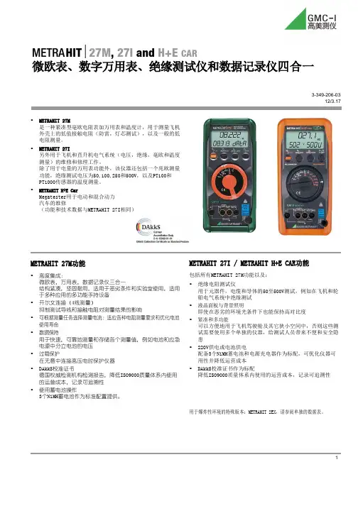
METRAHIT⏐27M, 27I and H+E CAR 微欧表、数字万用表、绝缘测试仪和数据记录仪四合一
严酷条件的防护 该设备采用非常紧凑,坚固的设计。除此之外,它还可以在 受到撞击或掉落时受到保护,免受损坏
通过带倾斜支架的软橡胶盖,橡胶材料还确保如果仪器放置在 振动表面上,仪器不会漂移。
技术参数
• 使用蓄电池操作 3个NiMH蓄电池作为标准配置提供。
METRAHIT 27I / METRAHIT H+E CAR功能
包括所有METRAHIT 27M功能以及:
• 绝缘电阻测试仪 用于元器件,电缆和导体的50至500V测试,例如在飞机和轮 船电气系统中绝缘测试
• 液晶面板与背景照明 即使在恶劣的环境光条件下也能保持高对比度
DIN EN 61326-1 VDE 0843-20-1
• 紧凑和多功能 可以方便地用于飞机驾驶舱及其它狭小空间中,否则这些测 试需要使用多个单独的仪器,给测试人员带来不便和安全隐 患
• 220V供电或电池供电 配备3个NiMH蓄电池和电源充电器作为标配,可优化仪器可 用性并降低运营成本
• DAkkS校准证书作为标配 降低ISO9000质量体系内使用的运营成本,记录可追溯性
仪器还可测量和记录绝缘电阻(仅限METRAHIT 27I),测试电压
可分步选择,例如为了测试飞机,远洋船舶等车载电气系统
对操作者的保护
的电阻,以及测试过电压避雷器等等更多。
METRAHIT 27可保护短暂错误连接到600v以内被测设备,通过内
部的保护电路实现。
测试功能和自动功能
所有METRAHIT 27仪器都配有二极管和导通性测试功能, 以及自动和手动测量范围选择和电池自动关闭功能。
LM27CIM5-2HJNOPB;LM27CIM5X-1HJNOPB;LM27CIM5X-2HJNOPB;LM27CIM5X-ZHJNOPB;中文规格书,Datasheet资料
LM27LM27 SOT-23, ±3°C Accurate, 120°C-150°C Factory Preset ThermostatLiterature Number: SNIS124BLM27SOT-23,±3˚C Accurate,120˚C-150˚C Factory Preset ThermostatGeneral DescriptionThe LM27is a precision,single digital-output,low-power thermostat comprised of an internal reference,DAC,tem-perature sensor and comparator.Utilizing factory program-ming,it can be manufactured with different trip points as well as different digital output functionality.The trip point (T OS )can be preset at the factory to any temperature in the range of +120˚C to +150˚C in 1˚C increments.The LM27has one digital output (OS/OS/US/US),one digital input (HYST)and one analog output (V TEMP ).The digital output stage can be preset as either open-drain or push-pull.In addition,it can be factory programmed to be active HIGH or LOW.The digital output can be factory programmed to indicate an over tem-perature shutdown event (OS or OS)or an under tempera-ture shutdown event (US or US).When preset as an over-temperature shutdown (OS)it will go LOW to indicate that the die temperature is over the internally preset T OS and go HIGH when the temperature goes below (T OS –T HYST ).Simi-larly,when preprogrammed as an undertemperature shut-down (US)it will go HIGH to indicate that the temperature is below T US and go LOW when the temperature is above (T US +T HYST ).The typical hysteresis,T HYST ,can be set to 2˚C or 10˚C and is controlled by the state of the HYST pin.A V TEMP analog output provides a voltage that is proportional to temperature and has a −10.7mV/˚C output slope.Currently,there are several standard parts available,see ordering information for details.For other part options,con-tact a National Semiconductor Distributor or Sales Repre-sentative for information on minimum order qualification.The LM27is currently available in a 5-lead SOT-23package.Applicationsn Microprocessor Thermal Management n Appliancesn Portable Battery Powered Systems n Fan Controln Industrial Process Control n HVAC SystemsnElectronic System ProtectionFeaturesn Internal comparator with pin selectable 2˚C or 10˚C hysteresisn No external components requiredn Open-drain or push-pull digital output;supports CMOS logic levelsn Internal temperature sensor with V TEMP output pin n V TEMP output allows after-assembly system testingn Internal voltage reference and DAC for trip-point setting n Currently available in 5-pin SOT-23plastic package n Excellent power supply noise rejectionKey Specificationsj Power Supply Voltage 2.7V to 5.5V j Power Supply Current 40µA(max)15µA(typ)j Hysteresis Temperature2˚C or 10˚C(typ)j Temperature Trip Point Accuracy±3˚C (max)LM27CIM5-2HJ Simplified Block Diagram and Connection Diagram20030701The LM27CIM5-2HJ has a fixed trip point of 140˚C.For other trip point and output function availability,please see ordering information or contact National Semiconductor.©2006National Semiconductor Corporation teristics Section.Contact National Semiconductor for other set points and output options.Order NumberTop Mark NS PackageNumber Trip Point Setting Output FunctioBulk Rail 3000Units in Tape&ReelLM27CIM5-ZHJ LM27CIM5X-ZHJ TZHJ MA05B120˚C Open Drain OS LM27CIM5-1HJ LM27CIM5X-1HJ T1HJ MA05B130˚C Open Drain OS LM27CIM5-2HJ LM27CIM5X-2HJ T2HJ MA05B140˚C Open Drain OSConnection Diagram20030702Pin DescriptionsPin Number Pin Name Function Connection 1HYST Hysteresis control,digitalinputGND for10˚C or V+for2˚C2GND Ground,connected to theback side of the die throughlead frame.System GND3V TEMP Analog output voltageproportional to temperature Leave floating or connect to a high impe node.4V+Supply input 2.7V to5.5V with a0.1µF bypass capacFor PSRR information see Section TitledNOISE CONSIDERATIONS.5OS Overtemperature Shutdownopen-drain active lowthermostat digital output Controller interrupt,system or power sup shutdown;pull-up resistor≥10kΩOS Overtemperature Shutdowntotem-pull active highthermostat digital output Controller interrupt,system or power sup shutdownUS Undertemperature Shutdownopen-drain active lowthermostat digital output System or power supply shutdown;pull-resistor≥10kΩUS Undertemperature Shutdowntotem-pull active highthermostat digital outputSystem or power supply shutdown Note:pin5functionality and trip point setting are programmed during LM27manufacture.2Input Voltage 6.0V Input Current at any pin(Note2)5mA Package Input Current(Note2)20mA Package Dissipation at T A=25˚C(Note3)500mW Soldering InformationSOT23PackageVapor Phase(60seconds) Infrared(15seconds)215˚C 220˚CStorage Temperature−65˚C to+150˚CMachine Model250VOperating Ratings(Note1)Specified Temperature Range T MIN≤T A≤T MAX LM27CIM−40˚C≤T A≤+150˚C Positive Supply Voltage(V+)+2.7V to+5.5V Maximum V OUT+5.5VLM27Electrical CharacteristicsThe following specifications apply for V+=2.7V DC to5.5V DC,and V TEMP load current=0µA unless otherwise specified.Bold-face limits apply for T A=T J=T MIN to T MAX;all other limits T A=T J=25˚C unless otherwise specified.Typical LM27CIM Units Symbol Parameter Conditions(Note6)Limits(Limits)(Note7)Temperature SensorTrip Point Accuracy(IncludesV REF,DAC,Comparator Offset,and Temperature Sensitivityerrors)+120˚C<T A<+150˚C±3˚C(max)Trip Point Hysteresis HYST=GND10˚CHYST=V+2˚C V TEMP Output TemperatureSensitivity−10.82mV/˚CV TEMP Temperature Sensitivity Error to Equation:V O=(−3.552x10⁻⁶x(T−30)2+ (−10.695x10⁻³x(T−30))+1.8386V −30˚C≤T A≤150˚C,2.7V≤V+≤5.5V±3˚C(max)−55˚C≤T A≤150˚C,4.5V≤V+≤5.5V±3˚C(max) T A=25˚C±2.5˚C(max)V TEMP Load Regulation Source≤1µA0.070mVSink≤40µA0.7mV(max) V TEMP Line Regulation+2.7V≤V+≤+5.5V,−30˚C≤T A≤+120˚C−0.2mV/VI S Supply Current152240µA(max)µA(max)Digital Output and InputI OUT(“1”)Logical“1”Output LeakageCurrent(Note9)V+=+5.0V0.0011µA(max)V OUT(“0”)Logical“0”Output Voltage I OUT=+1.2mA andV+≥2.7V;I OUT=+3.2mA andV+≥4.5V;(Note8)0.4V(max)V OUT(“1”)Logical“1”Push-Pull OutputVoltage I SOURCE=500µA,V+≥2.7V0.8x V+V(min)I SOURCE=800µA,V+≥4.5VV+−1.5V(min)V IH HYST Input Logical”1“ThresholdVoltage0.8x V+V(min)V IL HYST Input Logical”0“ThresholdVoltage0.2x V+V(max)3functional,but do not guarantee specific performance limits.For guaranteed specifications and test conditions,see the Electrical Characteristics.The gu specifications apply only for the test conditions listed.Some performance characteristics may degrade when the device is not operated under the li conditions.Note2:When the input voltage(V I)at any pin exceeds the power supply(V I<GND or V I>V+),the current at that pin should be limited to5mA.Th maximum package input current rating limits the number of pins that can safely exceed the power supplies with an input current of5mA to four.Unde operating conditions the maximum current that pins2,4or5can handle is limited to5mA each.Note3:The maximum power dissipation must be derated at elevated temperatures and is dictated by T Jmax(maximum junction temperature),θJA(ju ambient thermal resistance)and T A(ambient temperature).The maximum allowable power dissipation at any temperature is P D=(T Jmax–T A)/θJA or the given in the Absolute Maximum Ratings,whichever is lower.For this device,T Jmax=150˚C.For this device the typical thermal resistance(θJA)of the package types when board mounted follow:Package TypeθJASOT23-5,MA05B250˚C/WNote4:The human body model is a100pF capacitor discharge through a1.5kΩresistor into each pin.The machine model is a200pF capacitor discharged into each pin.Note5:See the URL”/packaging/“for other recommendations and methods of soldering surface mount devices.Note6:Typicals are at T J=T A=25˚C and represent most likely parametric norm.Note7:Limits are guaranteed to National’s AOQL(Average Outgoing Quality Level).Note8:Care should be taken to include the effects of self heating when setting the maximum output load current.The power dissipation of the LM27would by1.28mW when I OUT=3.2mA and V OUT=0.4V.With a thermal resistance of250˚C/W,this power dissipation would cause an increase in the die temperature 0.32˚C due to self heating.Self heating is not included in the trip point accuracy specification.Note9:The1µA limit is based on a testing limitation and does not reflect the actual performance of the part.Expect to see a doubling of the current for ev increase in temperature.For example,the1nA typical current at25˚C would increase to16nA at85˚C.Part Number TemplateThe series of digits labeled xyz in the part number LM27CIM-xyz,describe the set point value and the function of the ou follows:The place holders xy describe the set point temperature as shown in the following table.x(10x)y(1x)Temperature(˚C) -H0-J1-K2-L3-N4-P5-R6x(10x)y(1x)Temperature(˚C -S7-T8-V9Z-121-132-143-15The value of z describes the assignment/function of the output as shown in the following table:Active-Low/High Open-Drain/Push-Pull OS/US Value of z Digital Output Function000J Active-Low,Open-Drain,OS out 001K Active-Low,Open-Drain,US out 110L Active-High,Push-Pull,OS outp 111N Active-High,Push-Pull,US outpFor example:•the part number LM27CIM5-2SJ has T OS=147˚C,and programmed as an active-low open-drain overtemperature shu output.•the part number LM27CIM5-ZLN has T US=123˚C,and programmed as an active-high,push-pull undertemperature shu output.Active-high open-drain and active-low push-pull options are available,please contact National Semiconductor for more in tion.4LM27OPTIONSThe LM27can be factory programmed to have a trip point anywhere in-between 120˚C to 150˚C.Applications HintsAFTER-ASSEMBLY PCB TESTINGThe LM27’s V TEMP output allows after-assembly PCB testing by following a simple test procedure.Simply measuring the V TEMP output voltage will verify that the LM27has been assembled properly and that its temperature sensing cir-cuitry is functional.The V TEMP output has very weak drive capability that can be overdriven by 1.5mA.Therefore,one can simply force the V TEMP voltage to cause the digital output to change state,thereby verifying that the comparator and output circuitry function after assembly.Here is a sample test procedure that can be used to test the LM27CIM5X-2HJ which has a 140˚C trip point.1.Turn on V +and measure V TEMP .Then calculate thetemperature reading of the LM27using the equation:V O =(−3.552x10⁻⁶x(T−30)2)+(−10.69576x10⁻³x(T−30))+1.8386V(1)or(2)2.Verify that the temperature measured in step one iswithin (±3˚C +error of reference temperature sensor)of the ambient/board temperature.The ambient/board tem-perature (reference temperature)should be measured using an extremely accurate calibrated temperature sen-sor,which is in close proximity to and mounted on the same PCB as the LM27perhaps even touching the GND lead of the LM27if possible.The LM27will sence theboard temperature not the ambient temperature (see Section Titled Mounting Considerations )3.A.Observe that OS is high.B.Drive V TEMP to ground.C.Observe that OS is now low.D.Release the V TEMP pin.E.Observe that OS is now high.4.A.Observe that OS is high.B.Drive V TEMP voltage down gradually.C.When OS goes low,note the V TEMP voltage.D.V TEMP Trig =V TEMP at OS trigger (HIGH->LOW)E.Calculate Ttrig using Equation (2).5.A.Gradually raise V TEMP until OS goes HIGH.NoteV TEMP .B.Calculate T HYST using Equation (2).V TEMP LOADINGThe V TEMP output has very weak drive capability (1µA source,40µA sink).So care should be taken when attaching circuitry to this pin.Capacitive loading may cause the V TEMP output to oscillate.Simply adding a resistor in series as shown in Figure 2will prevent oscillations from occurring.To determine the value of the resistor follow the guidelines given in Table 1.The same value resistor will work for either placement of the resistor.If an additional capacitive load is placed directly on the LM27output,rather than across C LOAD ,it should be at least a factor of 10smaller than C LOAD .20030712LM27-__J 20030713LM27-__K20030714LM27-__L20030715LM27-__NFIGURE 1.Output Pin Options Block Diagrams5TABLE 1.Resistive compensation for capacitiveloading of V TEMPC LOAD R (Ω)≤100pF 01nF 820010nF 3000100nF 1000≥1µF430NOISE CONSIDERATIONSThe LM27has excellent power supply noise rejection.Listed below is a variety of signals used to test the LM27power supply rejection.False triggering of the output was not ob-served when these signals where coupled into the V+pin of the LM27.•square wave 400kHz,1Vp-p •square wave 2kHz,200mVp-p•sine wave 100Hz to 1MHz,200mVp-pTesting was done while maintaining the temperature of the LM27one degree centigrade way from the trip point with the output not activated.MOUNTING CONSIDERATIONSThe LM27can be applied easily in the same way as other integrated-circuit temperature sensors.It can be glued or cemented to a surface.The temperature that the LM27is sensing will be within about +0.06˚C of the surface tempera-ture to which the LM27’s leads are attached to.actual temperature measured would be at an interm temperature between the surface temperature and temperature.To ensure good thermal conductivity,the backside LM27die is directly attached to the GND pin (pin 2temperatures of the lands and traces to the other leads LM27will also affect the temperature that is being se Alternatively,the LM27can be mounted inside a seale metal tube,and can then be dipped into a bath or sc into a threaded hole in a tank.As with any IC,the LM accompanying wiring and circuits must be kept insulat dry,to avoid leakage and corrosion.This is especially the circuit may operate at cold temperatures where co sation can occur.Printed-circuit coatings and varnishe as Humiseal and epoxy paints or dips are often u ensure that moisture cannot corrode the LM27or its c tions.The junction to ambient thermal resistance (θJA )is t rameter used to calculate the rise of a part’s junctio perature due to its power dissipation.For the LM equation used to calculate the rise in the die junctio perature is as follows:where T A is the ambient temperature,V +is the power voltage,I Q is the quiescent current,I L_TEMP is th current on the V TEMP output,V DO is the voltage on the output,and I DO is the load current on the digital output the LM27’s junction temperature is the actual tempe being measured,care should be taken to minimize th current that the LM27is required to drive.The tables shown in Figure 3summarize the therma tance for different conditions and the rise in die tempe of the LM27without any loading on V TEMP and a 10k resistor on an open-drain digital output with a 5.5V supply.20030717a)R in series with capacitor20030718b)R in series with signal pathFIGURE 2.Resistor placement for capacitive loadingcompensation of V TEMPSOT23-5no heat sink SOT23-5small heat s θJA (˚C/W)T J −T A (˚C)θJA (˚C/W)T J (˚Still Air 2500.11TBD TMoving AirTBDTBDTBDTFIGURE 3.Thermal resistance (θJA )and temperarise due to self heating (T J −T A ) 620030703Note:The fan’s control pin has internal pull-up.The10k pull-down sets a slow fan speed.When the output of the LM27goes low,the fan will speed up.FIGURE4.Two Speed Fan Speed Control20030720FIGURE5.Fan High Side Drive20030721FIGURE6.Fan Low Side Drive7FIGURE7.Audio Power Amplifier Thermal Protection20030723FIGURE8.Simple Thermostat85-Lead Molded SOT-23Plastic Package,JEDECOrder Number LM27CIM5or LM27CIM5XNS Package Number MA05BNational does not assume any responsibility for use of any circuitry described,no circuit patent licenses are implied and National reserves the right at any time without notice to change said circuitry and specifications.For the most current product information visit us at .LIFE SUPPORT POLICYNATIONAL’S PRODUCTS ARE NOT AUTHORIZED FOR USE AS CRITICAL COMPONENTS IN LIFE SUPPORT DEVICES OR SYSTEMS WITHOUT THE EXPRESS WRITTEN APPROVAL OF THE PRESIDENT AND GENERAL COUNSEL OF NATIONAL SEMICONDUCTOR CORPORATION.As used herein:1.Life support devices or systems are devices or systemswhich,(a)are intended for surgical implant into the body,or(b)support or sustain life,and whose failure to perform whenproperly used in accordance with instructions for useprovided in the labeling,can be reasonably expected to resultin a significant injury to the user.2.A critical component is any component of a life supportdevice or system whose failure to perform can be reasonablyexpected to cause the failure of the life support device orsystem,or to affect its safety or effectiveness.BANNED SUBSTANCE COMPLIANCENational Semiconductor follows the provisions of the Product Stewardship Guide for Customers(CSP-9-111C2)and Banned Substances and Materials of Interest Specification(CSP-9-111S2)for regulatory environmental compliance.Details may be found at: /quality/green.Lead free products are RoHS compliant.National SemiconductorAmericas CustomerSupport CenterEmail:new.feedback@Tel:1-800-272-9959National SemiconductorEurope Customer Support CenterFax:+49(0)180-5308586Email:europe.support@Deutsch Tel:+49(0)6995086208English Tel:+44(0)8702402171Français Tel:+33(0)141918790National SemiconductorAsia Pacific CustomerSupport CenterEmail:ap.support@National SemiconductorJapan Customer Support CenterFax:81-3-5639-7507Email:jpn.feedback@分销商库存信息: NATIONAL-SEMICONDUCTORLM27CIM5-2HJ/NOPB LM27CIM5X-1HJ/NOPB LM27CIM5X-2HJ/NOPBLM27CIM5X-ZHJ/NOPBLM27CIM5-1HJ/NOPB LM27CIM5-ZHJ/NOPB。
NSD-2101-ASST;中文规格书,Datasheet资料
Fluke 27II_用户手册中文版(数字万用表)
®
27 II/28 II
Digital Multimeters
用户手册
September 2009, Rev. 1, 10/10 (Simplified Chinese) © 2009, 2010 Fluke Corporation. All rights reserved. Specifications are subject to change without notice. All product names are trademarks of their respective companies.
终生有限保证
Fluke 保证每一台 Fluke 20、70、80、170、180 和 280 系列的 DMM,其用料和做工都是终生毫无瑕疵的。此处所 谓的 “终生 ”是指 Fluke 终止制 造本产品后七年,但本项保证期应自产品购买日起至少十年内有效。本项保证不 包括保 险丝、可弃置的电池以及因疏忽、误用、污染、改 变、意外或非正常状况下的使用或处理所造成的损坏 (包括 使用产品规范以外的测量所引起的故障或机械部件的正常损耗)。本项保证仅适 用于原购买者并且不 得转让。 自购买日起十年内,本保证也包括 LCD。十年以后直到仪表的终生,Fluke 将以收费的方式更换 DMM 的 LCD (根据 当时该组件的成本价格收 取费用)。 欲建立原购买者与购买日期的根据,请填妥并寄回产品所附上的注册登记卡,或在 上注册产 品。对于从 Fluke 授权销售处以适当的国际价格所购买而损坏的产品,Fluke 可选择免费修理、更换或以原购买价 退款的方式处理该产品。若产 品是从一个国家购买却被送到其它地区修理,Fluke 保留收取修理/更换零件的进口费用的权利。 如果发现产品损坏,请和最靠近您的 Fluke 授权服务中心联络以取得同意退回产品的信息,然后请把产品寄到该服务中心。请说明遭遇到困难 的地方,并预付邮资和保险费(目的地离岸价格)。Fluke 不负责产品在运输 上的 损坏。对保修产品的修理或更换,Fluke 将负责回邮的运输费 用。对非保修产品的修理,Fluke 会对修理费用 作出估价并取得您的同意以后才进行修理,修理后 Fluke 将向您收取修理和回邮的运输费用。 本项保证是您仅有的补偿。除此以外,没有任何其它明示或默示的保证(包括保证某一特殊目的的适应性)。 凡因任何原因或原理而引起的特别、间接、附带或继起的损坏或损失(包括数据的损失),FLUKE 也一概不予 负责。授权的代理商无权代表 Fluke 延长本项 保证。由于某些州不允许对默示保证及附带或继起的损坏有所限 制,本保证的限制或许不适 用于您。 若本保证的任何条款被 法庭或其它具有司法管辖权的决定者裁定为不 适用或不可执行时,该项裁定将不得影响其它条款的有效性或执行性。
OPA27中文资料
®
OPA27, 37
2
SPECIFICATIONS
At VCC = ±15V and TA = +25°C, unless otherwise noted.
PARAMETER
CONDITIONS
OPA27/37G
MIN
TYP
MAX
UNITS
INPUT VOLTAGE (1) Input Offset Voltage Average Drift (2) Supply Rejection
ABSOLUTE MAXIMUM RATINGS
Supply Voltage ................................................................................... ±22V Internal Power Dissipation (1) ........................................................ 500mW Input Voltage ...................................................................................... ±VCC Output Short-Circuit Duration (2) ................................................. Indefinite Differential Input Voltage (3) ............................................................. ±0.7V Differential Input Current (3) ........................................................... ±25mA Storage Temperature Range .......................................... –55°C to +125°C Operating Temperature Range ......................................... –40°C to +85°C Lead Temperature:
- 1、下载文档前请自行甄别文档内容的完整性,平台不提供额外的编辑、内容补充、找答案等附加服务。
- 2、"仅部分预览"的文档,不可在线预览部分如存在完整性等问题,可反馈申请退款(可完整预览的文档不适用该条件!)。
- 3、如文档侵犯您的权益,请联系客服反馈,我们会尽快为您处理(人工客服工作时间:9:00-18:30)。
/
programming algorithms and voltages. The AT27LV020A programs in exactly the same way as a standard, 5V Atmel AT27C020, and uses the same programming equipment.
2Mb (256K x 8) Low Voltage, One-time Programmable, Read-only Memory
Atmel AT27LV020A
1.
Description
The Atmel AT27LV020A is a high-performance, low-power, low-voltage, 2,097,152-bit, one-time programmable, read-only memory (OTP EPROM) organized as 256K by 8 bits. It requires only one supply in the range of 3.0 to 3.6V in normal read mode operation, making it ideal for fast, portable systems using battery power. The Atmel innovative design techniques provide fast speeds that rival 5V parts, while keeping the low power consumption of a 3V supply. At VCC = 3.0V, any byte can be accessed in less than 120ns. With a typical power dissipation of only 18mW at 5MHz and VCC = 3.3V, the AT27LV020A consumes less than one-fifth the power of a standard, 5V EPROM. Standby mode supply current is typically less than 1µA at 3.3V. The AT27LV020A is available in an industry-standard, JEDEC-approved, one-time programmable (OTP) PLCC package. All devices feature two-line control (CE, OE) to give designers the flexibility to prevent bus contention. The AT27LV020A operating with VCC at 3.0V produces TTL-level outputs that are compatible with standard TTL logic devices operating at VCC = 5.0V. The device is also capable of standard, 5V operation, making it ideally suited for dual supply range systems or card products that are pluggable in both 3V and 5V hosts. The AT27LV020A has additional features to ensure high quality and efficient production use. The rapid programming algorithm reduces the time required to program the part and guarantees reliable programming. Programming time is typically only 100µs/byte. The integrated product identification code electronically identifies the device and manufacturer. This feature is used by industry standard programming equipment to select the proper
2.
Pin configurations
Pin name A0 - A17 O0 - O7 CE OE PGM NC Function Addresses Outputs Chip enable Output enable Program strobe No connect
A7 A6 A5 A4 A3 A2 A1 A0 O0
Features
• Fast read ccess time – 120ns • Dual voltage range operation • • • • • • • • • •
– Low voltage power supply range, 3.0V to 3.6V, or – Standard power supply range, 5V ± 10% Compatible with JEDEC standard Atmel® AT27C020 Low-power CMOS operation – 20µA max standby (less than 1µA, typical) for VCC = 3.6V – 29mW max active at 5MHz for VCC = 3.6V JEDEC standard package – 32-lead PLCC High-reliability CMOS technology – 2,000V ESD protection – 200mA latchup immunity Rapid programming algorithm – 100µs/byte (typical) Two-line control CMOS- and TTL-compatible inputs and outputs – JEDEC standard for LVTTL Integrated product identification code Industrial temperature range Green (Pb/halide-free) packaging option
Figure 3-1. Block diagram
2
Atmel AT27LV020A
0549H–EPROM–4/11
/
Atmel AT27LV020A 4. Absolute maximum ratings*
Temperature under bias . . . . . . . . . . . . . . . -40C to +85C Storage temperature . . . . . . . . . . . . . . . . -65C to +125C Voltage on any pin with with respect to ground . . . . . . . . . . . . . . -2.0V to +7.0V(1) Voltage on A9 with respect to ground . . . . . . . . . . . . . . . . . . -2.0V to +14.0V(1) VPP supply voltage with respect to ground . . . . . . . . . . . . . . . . . . -2.0V to +14.0V(1) Notes: 1. Minimum voltage is -0.6V DC, which may undershoot to -2.0V for pulses of less than 20ns. Maximum output pin voltage is VCC + 0.75V DC, which may be exceeded if certain precautions are observed (consult application notes), and which may overshoot to +7.0V for pulses of less than 20ns. *NOTICE: Stresses beyond those listed under “Absolute maximum ratings” may cause permanent damage to the device. This is a stress rating only, and functional operation of the device at these or any other conditions beyond those indicated in the operational sections of this specification is not implied. Exposure to absolute maximum rating conditions for extended periods may affect device reliability.
32-lead PLCC Top view
A12 A15 A16 VPP VCC PGM A17 O1 O2 GND O3 O4 O5 O6 14 15 16 17 18 19 20
5 6 7 8 9 10 11 12 13
4 3 2 1 32 31 30
29 28 27 26 25 24 23 22 21
A14 A13 A8 A9 A11 OE A10 CE O7