Bridge Rectifier datasheet-2010 T20XB60
单端反激式开关电源磁芯尺寸和类型的选择

单端反激式开关电源磁芯尺寸和类型的选择字体大小:大|中|小2008-08-28 12:53 - 阅读:1655 -评论:1单端反激式开关电源磁芯尺寸和类型的选择徐丽红王佰营wbymcs51.blog.bokee .netA、InternationalRectifier 公司--56KHz输出功率推荐磁芯型号0---10WEFD15SEF16EF16EPC17EE19EF(D)20EPC25EF(D)2510-20WEE19EPC19EF(D)20EE,EI22EF(D)25EPC2520-30WEI25EF(D)25EPC25EPC30EF(D)30ETD29EER28(L)30-50WEI28EER28(L)ETD29EF(D)30EER3550-70WEER28LETD34EER35ETD3970-100WETD34EER35ETD39EER40E21摘自 InternationalRectifier,AN1018- “应用 IRIS40xx 系列单片集成开关 IC 开关电源的反激式变压器设计”B、ELYTON公司型号输出功率( W)<5 5-10 10-20 20-50 50-100100-200 200-500 500-1KEI EI12.5 EI16 EI19 EI25 EI40--EI50 EI60EE EE13 EE16 EE19 EE25 EE40EE42 EE55 EE65EF EF12.6 EF16 EF20 EF25 EF30 EF32EFD -- EFD12 EFD15 EFD20 EFD25 EFD30EPC -- EPC13 EPC17 EPC19 EPC25 EPC30EER EER9.5 EER11 EER14.5 EER28 EER35 EER42EER49 --ETD ETD29 ETD34 ETD44ETD49 ETD54 --EP EP10 EP13 EP17 EP20 --RM RM4 RM5 RM6 RM10 RM12POT POT1107 POT1408 POT1811 POT2213POT3019 POT3622 POT4229 -- PQ -- -- -- PQ2016 PQ2625PQ3230 PQ3535 PQ4040EC ------------------------------ EC35 EC41 EC70摘自 PowerTransformers OFF-LINE Switch ModeAPPLICATION NOTES"Converter circuitas a function of S.M.P.S. output voltage (Vo) and output power (Po)"C、Fairchild Semiconductor 公司 -- 67KHzOutput Power EIcore EE core EPC core EER core0-10W EI12.5EE8EPC10EI16 EE10 EPC13EI19 EE13 EPC17EE1610-20WEI22EE19 EPC1920-30W EI25 EE22 EPC25 EER25.530-50WEI28 EE25EPC30 EER28EI3050-70W EI35 EE30 EER28L70-100W EI40 EE35 EER35100-150W EI50 EE40 EER40EER42150-200W EI60 EE50 EER49EE60The core quickselection table For universal input range, fs=67kHz and 12V singleoutput摘自: Application Note AN4140Transformer Design Consideration for off-lineFlybackTMConverters using Fairchild Power Switch (FPS)D 单端反激式变压器磁芯的选择公式 wbymcs51.blog.bokee .netVe =5555 * P / f式中:Ve --- 为磁芯的体积:Ve=Ae*Le;单位为:毫米立方;P ——为输入功率;单位为:瓦;f ——为开关频率;单位为:千赫兹;本公式假设:Bm=0.3T,Lg/Le=0.5%=气隙长度/磁芯等效长度;如果Lg/Le=气隙长度/磁芯等效长度=1%寸,又如何计算呢?(请考虑)输出功率、磁芯截面积和开关频率决定气隙,因为在反激式开关电源中气隙的体积大小决定储能的多少,频率决定能量传输的快慢;女口: EI25Ve=2050m3, Ae=42平方毫米,Le=49.4mm f=40KHz; n =0.75;Lg= 0.005*49.4 = 0.247mm --- 气隙长度Pin =Ve*F/5555 = 2050*40/5555 = 14.76W ;Pout = n *Pin= 0.75 * 14.76 = 11.07W;若: f=100KHz 则:Pout = 11.07W *(100/40) = 27.675W;。
MB10S;中文规格书,Datasheet资料

•Low leakage•Surge overload rating : 35 amperes peak.•Ideal for printed circuit board.•UL certified, UL #E111753 and E326243.Absolute Maximum Ratings * T A = 25°C unless otherwise noted* These ratings are limiting values above which the serviceability of any semiconductor device may by impaired.Thermal Characteristics* Device mounted on PCB with 0.5" x 0.5" (13 x 13 mm) lead lengthElectrical Characteristics T A = 25°C unless otherwise notedSymbolParameterValueUnitsV RRM Maximum Repetitive Reverse Voltage 1000V V RMS Maximum RMS Bridge Input Voltage 700V V R DC Reverse Voltage (Rated V R )1000V I F(AV)Average Rectified Forward Current, @ T A = 50°COn Glass-epoxy P .C.B. On Aluminum substrate 0.50.8A I FSM Non-Repetitive Peak Forward Surge Current 8.3 ms Single Half-Sine-Wave 35A T STG Storage Temperature Range -55 to +150°C T JOperating Junction Temperature-55 to +150°CSymbolParameter ValueUnitsP D Power Dissipation1.4W R θJA Thermal Resistance, Junction to Ambient,* per leg 85°C/W R θJLThermal Resistance, Junction to Lead,* per leg20°C/WSymbolParameterValueUnitsV F Forward Voltage, per bridge @ 0.5 A1.0V I RReverse Current, per leg @ Rated V R T A = 25°C T A = 125°C 5.00.5µA mA I 2t rating for fusing t < 8.3 ms5.0A 2s C TTotal Capacitance, per leg V R = 4.0V, f = 1.0MHz13pFSOIC-4Polarity symbols molded or marking on bodyFigure 4. Typical Junction Capacitance Per Leg Figure 3. Maximum Non-Repetitive PeakForward Surge Current Per LegFigure 5. Typical Forward VoltageCharacteristics Per LegThe following includes registered and unregistered trademarks and service marks, owned by Fairchild Semiconductor and/or its global subsidiaries, and is notAccuPower¥Auto-SPM¥Build it Now¥CorePLUS¥CorePOWER¥CROSSVOLT¥CTL¥Current Transfer Logic¥DEUXPEED®Dual Cool™ EcoSPARK®EfficientMax¥ESBC¥®Fairchild®Fairchild Semiconductor®FACT Quiet Series¥FACT®FAST®FastvCore¥FETBench¥FlashWriter®*FPS¥F-PFS¥FRFET®Global Power Resource SMGreen FPS¥Green FPS¥ e-Series¥G max¥GTO¥IntelliMAX¥ISOPLANAR¥MegaBuck¥MICROCOUPLER¥MicroFET¥MicroPak¥MicroPak2¥MillerDrive¥MotionMax¥Motion-SPM¥OptoHiT™OPTOLOGIC®OPTOPLANAR®®PDP SPM™Power-SPM¥PowerTrench®PowerXS™Programmable Active Droop¥QFET®QS¥Quiet Series¥RapidConfigure¥¥Saving our world, 1mW/W/kW at a time™SignalWise¥SmartMax¥SMART START¥SPM®STEALTH¥SuperFET¥SuperSOT¥-3SuperSOT¥-6SuperSOT¥-8SupreMOS®SyncFET¥Sync-Lock™®*The Power Franchise®TinyBoost¥TinyBuck¥TinyCalc¥TinyLogic®TINYOPTO¥TinyPower¥TinyPWM¥TinyWire¥TriFault Detect¥TRUECURRENT¥*P SerDes¥UHC®Ultra FRFET¥UniFET¥VCX¥VisualMax¥XS™* Trademarks of System General Corporation, used under license by Fairchild Semiconductor.DISCLAIMERFAIRCHILD SEMICONDUCTOR RESERVES THE RIGHT TO MAKE CHANGES WITHOUT FURTHER NOTICE TO ANY PRODUCTS HEREIN TO IMPROVE RELIABILITY, FUNCTION, OR DESIGN. FAIRCHILD DOES NOT ASSUME ANY LIABILITY ARISING OUT OF THE APPLICATION OR USE OF ANY PRODUCT OR CIRCUIT DESCRIBED HEREIN; NEITHER DOES IT CONVEY ANY LICENSE UNDER ITS PATENT RIGHTS, NOR THE RIGHTS OF OTHERS. THESE SPECIFICATIONS DO NOT EXPAND THE TERMS OF FAIRCHILD’S WORLDWIDE TERMS AND CONDITIONS, SPECIFICALLY THE WARRANTY THEREIN, WHICH COVERS THESE PRODUCTS.LIFE SUPPORT POLICYFAIRCHILD’S PRODUCTS ARE NOT AUTHORIZED FOR USE AS CRITICAL COMPONENTS IN LIFE SUPPORT DEVICES OR SYSTEMS WITHOUT THE EXPRESS WRITTEN APPROVAL OF FAIRCHILD SEMICONDUCTOR CORPORATION.As used herein:1. Life support devices or systems are devices or systems which, (a) areintended for surgical implant into the body or (b) support or sustain life, and (c) whose failure to perform when properly used in accordance with instructions for use provided in the labeling, can be reasonably expected to result in a significant injury of the user. 2. A critical component in any component of a life support, device, orsystem whose failure to perform can be reasonably expected to cause the failure of the life support device or system, or to affect its safety or effectiveness.ANTI-COUNTERFEITING POLICYFairchild Semiconductor Corporation's Anti-Counterfeiting Policy. Fairchild's Anti-Counterfeiting Policy is also stated on our external website, , under Sales Support.Counterfeiting of semiconductor parts is a growing problem in the industry. All manufacturers of semiconductor products are experiencing counterfeiting of their parts. Customers who inadvertently purchase counterfeit parts experience many problems such as loss of brand reputation, substandard performance, failed applications, and increased cost of production and manufacturing delays. Fairchild is taking strong measures to protect ourselves and our customers from the proliferation of counterfeit parts. Fairchild strongly encourages customers to purchase Fairchild parts either directly from Fairchild or from Authorized Fairchild Distributors who are listed by country on our web page cited above. Products customers buy either from Fairchild directly or from Authorized Fairchild Distributors are genuine parts, have full traceability, meet Fairchild's quality standards for handling and storage and provide access to Fairchild's full range of up-to-date technical and product information. Fairchild and our Authorized Distributors will stand behind all warranties and will appropriately address any warranty issues that may arise. Fairchild will not provide any warranty coverage or other assistance for parts bought from Unauthorized Sources. Fairchild is committed to combat this global problem and encourage our customers to do their part in stopping this practice by buying direct or from authorized distributors.PRODUCT STATUS DEFINITIONSDefinition of TermsDatasheet Identification Product Status Definition分销商库存信息: FAIRCHILDMB10S。
BSXE_datasheet_FINAL_4_4_08
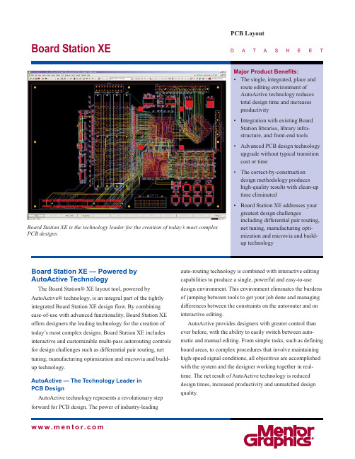
Board Station XEPCB LayoutD A T A S HE E Tw w w.m e n t o r.c o mBoard Station XE is the technology leader for the creation of today’s most complex PCB designs.Board Station XE — Powered by AutoActive TechnologyThe Board Station® XE layout tool, powered byAutoActive® technology, is an integral part of the tightly integrated Board Station XE design flow. By combining ease-of-use with advanced functionality, Board Station XE offers designers the leading technology for the creation of today’s most complex designs. Board Station XE includes interactive and customizable multi-pass autorouting controls for design challenges such as differential pair routing, net tuning, manufacturing optimization and microvia and build-up technology.AutoActive — The Technology Leader in PCB DesignAutoActive technology represents a revolutionary step forward for PCB design. The power of industry-leadingauto-routing technology is combined with interactive editing capabilities to produce a single, powerful and easy-to-use design environment. This environment eliminates the burdens of jumping between tools to get your job done and managing differences between the constraints on the autorouter and on interactive editing.AutoActive provides designers with greater control than ever before, with the ability to easily switch between auto-matic and manual editing. From simple tasks, such as defining board areas, to complex procedures that involve maintaining high-speed signal conditions, all objectives are accomplished with the system and the designer working together in real-time. The net result of AutoActive technology is reduced design times, increased productivity and unmatched design quality.What is AutoActive Technology?· A single, integrated, place and route editing environment that reducestotal design time and increasesproductivity·All physical rules and high-speed rules are maintained ·Correct-by-construction design that produces high-quality results withclean-up time eliminated ·Shape-based, true 45 degree routing ·The most advanced autorouting technology ever. Stop and start theautorouter at any time and all results will be correct-by-construction ·Dynamic clean-up of traces through the reduction of segments, preven-tion of acute angles and applicationof pad entry rulesDynamic Area FillsBoard Station XE automatically clears area fills around traces, vias and pads as the board is edited. Dynamic area fills are so fast, Board Station XE allows you to keep your area fillsturned on while you are doing all youredits. Moving a via pushes and shovesother vias, traces and area fills andconnectivity is automatically main-tained.Rules By AreaRules by area functionality greatlyimproves routing around BGAs andother fine-pitched parts. Rule areasrepresent complete rule sets that areobeyed by online and batch DRC and ininteractive and automatic routing. Ruleareas may be defined by layer and canbe assigned to any polygon, rectangle orcircle. Trace widths and clearancesautomatically change when traversinginto or out of the rule area. You mayalso change via sizes and spans in a rulearea to maximize route completion.Multiplow With Variable ViaPatternsBoard Station XE’s multiplow func-tionality allows you to simultaneouslyroute multiple nets, including differen-tial pairs, with true 45 degree routing. Itcan even handle routing through areasof staggered pins. Traces being routedwill push and shove the other vias andtraces out of the way and automaticallyclear area fills as needed. Changes canbe easily made to a variety of selectablevia patterns at the touch of a button,allowing enhanced flexibility forrouting into dense areas of a design.Dynamic Hazard ReviewDesign hazards are dynamicallydisplayed and may be individuallyselected and colored for easy identifica-tion. When a hazard is fixed, it isdynamically removed from the hazardlist.Leverages Legacy Board StationFlowBoard Station XE can be usedquickly and easily by existing BoardStation Layout customers. First, BoardStation XE uses the same libraries(geometries) as the legacy flow. BoardStation XE is integrated with he samefront-end tools and library managementsystem as the legacy tools. Finally,customers can easily import legacyBoard Station Layout designs intoBoard Station XE in order to start newdesigns from an existing one. This allgives customers access to the state-of-the-art layout environment using theirexisting library infrastructure and front-end tools.Board Station XE features market-leading technology for advanced interconnect.High-Speed Design with Board Station XEDesigners today are increasingly challenged by the need to manage signal quality in order to achieve system performance and reduce proto-type iterations. High-speed design with Board Station XE is an integrated part of the AutoActive design environment.Constraint DefinitionBoard Station XE handles an exten-sive set of constraints to meet high-speed performance requirements whether you’re routing interactively or automatically. A common constraint definition environment is shared between schematic capture and layout, allowing the evaluation of critical signals at any design stage. Constraints include same layer and adjacent layer differential pairs, controlled impedance, net scheduling and delay.Net TuningWhile routing interactively, graphic tuning aids are displayed for guidance. Nets modified out-of-tune during edits are automatically re-tuned. The Hazards dialog box dynamically updates as you edit nets, providing instant feedback relative to your constraints. Nets can also be tuned within an autoroute pass. Tuned nets are automatically maintained as you complete the design.Differential Pair RoutingRouting and editing differential pairs with Board Station XE is accomplished with speed and ease that will change your view of high-speed design. Pair spacing rules can be established by both layer and net class. If one trace is edited, the other trace in the pair auto-matically moves with it. Adjacent layerdifferential pair routing capabilities addanother valuable option for routing crit-ical signals on a dense PCB.Xtreme TechnologyPatented Xtreme design technologyenables up to 15 clients to operate on acommon database simultaneously tointeractively develop PCB layouts(XtremePCB) and perform complexmulti-process auto-routing (XtremeAR)while reducing cycle times by up to70%.Advanced InterconnectRoutingThe challenges and of advancedinterconnect are prevalent today withBGA, CSP, COB and DCA packagesincreasing board density. Build-up andmicrovia structures used in these boarddesigns further complicate routing.Board Station XE, powered byAutoActive technology, offers theleading technology for advanced inter-connect designs.Board Station XE supports the defi-nition of complex via structure rulesand the routing of microvia geometries,including comprehensive via-in-padrules. Via spans between any two layersare possible. By moving beyond tradi-tional laminate layer pairing, BoardStation XE facilitates the design ofbuild-up structures on laminate toenable escape patterns from dense, highpin count devices. Build-up areas typi-cally have a smaller clearance than thelaminate beneath them. Board StationXE can establish delay values andclearances per via span to address theseissues. Additionally, Board Station XEfeatures true 45 degree routing for BGAfanout and staggered connectors,enabling localized rule definition tofacilitate escape paths from dense areas. Board Station XE features powerful differential pair routing and net tuning capabilities for advanced high-speed design.MF-04-081025940-wTo learn more about how Board Station XE can improve your PCB layout process, call Mentor Graphics to schedule a complete product demonstra-tion or visit our web site at / for the latest product news.Copyright © 2007 Mentor Graphics Corporation.Mentor Graphics, Board Station and AutoActive are registered trademarks and Xtreme and FabLink are trademarks of Mentor Graphics Corporation.All other trademarks mentioned in this document are trademarks of their respective owners.Printed on RecycledPaperFabLink XE Pro IntegrationBoard Station XE is tightly inte-grated with the new FabLink XE Pro manufacturing data preparation tools FabLink XE Pro provides a stand alone panel creation and editing environment for creating manufacturing data at the panel level that operates on a panel design database. In addition, it provides additional board level functionality,including detailed data views, search-able PDF output, copper balancing,various data outputs and Gerber In/Drill In capabilities. Manufacturing Output Validation (MOV) quickly and easily identifies out of date manufacturing data compared to the design data.FabLink XE interacts with design data at three levels: ManufacturingPreparation, Manufacturing Output and Documentation.Operating System Requirements •Windows 2000 •Windows Server 2003•Windows XP Professional •Linux•Red Hat Enterprise 3(Server & Desktop) •Red Hat Enterprise 4(Server & Desktop) •Red Hat Enterprise 5(Server & Desktop)•SUSE Enterprise 9(Server & Desktop)•SUSE Enterprise 10 (Server & Desktop)•Sun Solaris 2.8, 2.9, 2.10, X86Corporate Headquarters Mentor Graphics Corporation 8005 SW Boeckman Road Wilsonville, OR 97070-7777Phone: 503.685.7000Fax: 503.685.1204Sales and Product Information Phone: 800.547.3000Silicon ValleyMentor Graphics Corporation 1001 Ridder Park DriveSan Jose, California 95131 USA Phone: 408.436.1500Fax: 408.436.1501North American Support Center Phone: 800.547.4303EuropeMentor Graphics Deutschland GmbH Arnulfstrasse 20180634 Munich GermanyPhone: +49.89.57096.0Fax: +49.89.57096.40Pacific RimMentor Graphics (Taiwan)Room 1603, 16FInternational Trade BuildingNo. 333, Section 1, Keelung Road Taipei, Taiwan, ROC Phone: 886.2.87252000Fax: 886.2.27576027JapanMentor Graphics Japan Co., Ltd.Gotenyama Hills7-35, Kita-Shinagawa 4-chome Shinagawa-Ku, Tokyo 140 JapanPhone: 81.3.5488.3033Fax: 81.3.5488.3021。
Bridgelux Vesta Flex 双通道控制模块说明书

® Flex Product Data Sheet DS 460Vesta Flex PlatformThe Bridgelux Vesta Flex Dual Channel Driver and Control Module family is a bundled system, guaranteed to work together out of the box, that enables seamless control of the Bridgelux Vesta Series Tunable White Arrays and Modules. The Driver's high resolution dimming and tuning algorithm provides for smooth and flicker-free CCT tuning, dimming to 0.1%, and dim-to-off. These specification grade drivers and control modules are separate devices which, when connected via an ethernet cable, form a smart and flexible lighting control system. These Vesta Flex Control Modules are intended for use with a Vesta Flex Dual Channel Driver and to be factory installed as incorporated products. The platform offers a number of driver and control module options to choose from, enabling application flexibility and interoperability with third party systems. These different control modules support wired control protocols such as DALI-2 DT8 and 0-10V as well as wireless control protocols with WiFi and Bluetooth mesh. These platforms come with ready-built iOS and Android apps and web portals which provide for commissioning, light management, and services designed to expand the capability of modern lighting systems. Vesta Flex is a future-ready solution, designed to quickly adapt to new control systems without requiring luminaire recertification.Vesta Flex Platform OverviewVesta FlexControlModuleLighting systems with 0-10V wired control devicesThe Vesta Flex Dual 0-10V Control Module is compatible with industry standard 0-10V, 1-10V current sourcing or current sinking wired control devices. The Control Module provides for two-channel control of color temperature and intensity.Product Feature MapBridgelux Vesta Flex Control Module features a control port with an RJ45 terminal which enables plug-and-playconnectivity with any Vesta Flex Dual Channel Driver control port. The Control Module receives auxiliary power from the Driver via the RJ45 control port and communicates with the Driver via a dual channel PWM signal.The control module receives its control inputs via two pairs of analog 0-10V signal wires, one pair for intensity dimming and one pair for CCT tuning.Please visit for more information on compatible Vesta Flex Dual Channel Driver and Vesta Series Tunable White arrays and modules.Product NomenclatureThe part number designation for Bridgelux Vesta Flex Dual 0-10V Control Module is explained as follows:1,2,3,4 5,6,7, 9,10,11, 14,15, 16Product FamilyBXCS = Control & SensorsProduct Version 02 = Version 2Output Protocol P = PWMMounting holesInput Voltage12 = 12VBXCSN2P02A----Control port compatible with Ves-ta Flex Dual Channel Driver12AIntegrated SensorsN = NoneOutput Channels2 = Dual Channel (WW, CW)Control InputA = Analog (Dual 0-10V)Product Generation A = Generation A Poke-in connector for 0-10V controlsTable 2:Electrical CharacteristicsElectrical CharacteristicsVesta Flex Control Modules are designed to connect and communicate with all Vesta Flex Dual Channel Drivers out of the box. Any 8P8C category ethernet cable with RJ45 connectors may be used to connect the Control Module and the Driver via the RJ45 port. The communication between the control module and the driver is asymmetric. The Vesta Flex Dual Channel Driver will not work without this asymmetric communication signal from the Vesta Flex control module.The Vesta Flex Driver automatically detects which control module is connected to it and adjusts its settings accordingly. This feature allows to simply plug-and-play any Vesta Flex Control Module with any Vesta Flex Dual Channel Driver regardless of the chosen communication protocol on the Vesta Flex Control Module.Bridgelux recommends the use of an ethernet cable that is commonly available and recognized by the Telecommunica-tions Industries Association (TIA), e.g. Cat 5e, Cat 6 and Cat 6a cables.The maximum length of such an ethernet cable is 300m.Control Port ConnectionNotes for Figure 1:1. When the Vesta Flex 0-10V Control Module is dimmed down and thesignal voltage reaches 0.85V, then the Driver output power goes tozero and the Driver goes in standby mode. When the Control Module is dimmed up and the dimming control signal voltage reaches 0.95V, then the Driver exits standby mode and turns on its output power at minimum output current. That hysteresis prevents any potental flicker when the dimming control voltage drops below 1.0V.Control CharacteristicsTable 4:Control Signal CharacteristicsMinimum Dimming LevelOffOn from standby mode Offand standby modeDimming startFigure 1: Control Signal Dim-To-Off Hysteresis Lowest CCT Tuning LimitTuning startFigure 2: Control Signal at Lowest CCT LimitNotes for Figure 2:1. When the Vesta Flex 0-10V Control Module is tuned to its lowest CCT limit and the signal voltage drops below 1.0V, then Driver output maintains its current state resulting in a constant CCT at the lowest limit.Terminal ConfigurationInput TerminalFigure 3: Terminal ConfigurationControl PortNotes for Table 6:1. The - 0-10V Dim and the - 0-10V CCT terminals are internally connected to a common ground.Mechanical Characteristics Table 7:Control Module Mechanical CharacteristicsEnvironmental and Regulatory StandardsDesign ResourcesApplication NotesPlease contact your Bridgelux sales representative for assistance on obtaining application support when designing with the Bridgelux Vesta Flex Dual Channel Driver and Control Modules. For a list of available resources, visit .3D CAD ModelsCAD models depicting the Vesta Flex Wireless Control module are available in both IGES and STEP formats. Please contact your Bridgelux sales representative for assistance.PrecautionsCAUTION: PRODUCT HANDLINGHandle the Vesta Flex Control Module with care to prevent any damage from mechanical shock.It is recommended to handle this module in a static-free environment.Do not open or disassemble the product.To maintain product warranty, the installer is responsible for ensuring that the module's operating conditions do not exceed the maximum conditions stated within this data sheet.CAUTION: PRODUCT INSTALLATIONIncorrect installation of the Vesta Flex wireless control module can cause irreparable damage to the module, connected Vesta Flex Driver and/or connected LEDs.When connecting the Vesta Flex wireless control module with the Vesta Flex Dual Channel Driver, make sure that the RJ45 connectors are locked in the RJ45 ports.The product is intended for factory installation in a panel or into a controlled equipment.DisclaimersMINOR PRODUCT CHANGE POLICYThe rigorous qualification testing on products offered by Bridgelux provides performance assurance. Slight cosmetic changes that do not affect form, fit, or function may occur as Bridgelux continues product optimization.11About Bridgelux: Bridging Light and Life™© 2020 Bridgelux, Inc. All rights reserved 2020. Product specifications are subject to change without notice. Bridgelux, the Bridgelux stylized logo design and Vesta are regis -tered trademarks of Bridgelux, Inc. Bridging Light and Life is a trademark of Bridgelux, Inc. All other trademarks are the property of their respective owners.Bridgelux Vesta Flex Dual 0-10V Control Module Data Sheet DS460 Rev. B (10/2020)46430 Fremont BlvdFremont, CA 94538 USATel (925) 583-8400At Bridgelux, we help companies, industries and people experience the power and possibilityof light. Since 2002, we’ve designed LED solutions that are high performing, energy efficient,cost effective and easy to integrate. Our focus is on light’s impact on human behavior, deliveringproducts that create better environments, experiences and returns—both experiential andfinancial. And our patented technology drives new platforms for commercial and industrialluminaires.For more information about the company, please visit /Bridgelux /Bridgelux /user/Bridgelux /company/bridgelux WeChat ID: BridgeluxInChina。
MB1S

LIFE SUPPORT POLICY
FAIRCHILD’S PRODUCTS ARE NOT AUTHORIZED FOR USE AS CRITICAL COMPONENTS IN LIFE SUPPORT DEVICES OR SYSTEMS WITHOUT THE EXPRESS WRITTEN APPROVAL OF FAIRCHILD SEMICONDUCTOR CORPORATION.
™*
®
Fairchild® Fairchild Semiconductor® FACT Quiet Series™ FACT® FAST® FastvCore¥ FETBench¥ FlashWriter®* FPS¥
F-PFS¥ FRFET® Global Power ResourceSM Green FPS¥ Green FPS¥ e-Series¥ Gmax™ GTO¥ IntelliMAX¥ ISOPLANAR¥ MegaBuck™ MICROCOUPLER¥ MicroFET¥ MicroPak¥ MillerDrive™ MotionMax™ Motion-SPM™ OPTOLOGIC® OPTOPLANAR®
Value 1.4 85 20
Electrical Characteristics TA = 25°C unless otherwise noted
Symbol
Parameter
VF
Forward Voltage, per bridge @ 0.5 A
IR
Reverse Current, per :
1. Life support devices or systems are devices or systems which, (a) are intended for surgical implant into the body or (b) support or sustain life, and (c) whose failure to perform when properly used in accordance with instructions for use provided in the labeling, can be reasonably expected to result in a significant injury of the user.
MBR20100CT-BP;中文规格书,Datasheet资料
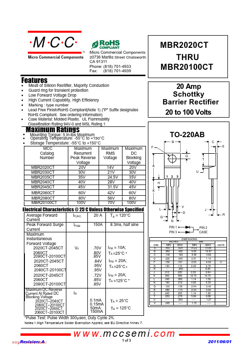
THRU 20Amp Features• Meatl of Silicon Rectifier, Majority Conduct i on • Guard ring for transient protection • Low Forward Voltage Drop• High Current Capability, High Efficiency • Marking : type numberMCC Catalog Number Maximum Recurrent Peak Reverse Voltage Maximum RMS Voltage Maximum DC BlockingVoltageMBR2020CT 20V 14V 20V MBR2030CT 30V 21V 30V MBR2035CT 35V 24.5V 35V MBR2040CT 40V 28V 40V MBR2045CT 45V 31.5V 45V Electrical Characteristics @ 25°C Unless Otherwise SpecifiedAverage Forward CurrentI F(AV)20 A T A = 120°C Peak Forward Surge Current I FSM 150A 8.3ms, half sineMaximum Instantaneous Forward Voltage2020CT-2045CT 2060CTV F .70V.80V *Pulse Test: Pulse Width 300µsec, Duty Cycle 2%2020CT-2045CT2060CT.84V .95V 2080CT-20100CT .95VI FM = 20A;T A =25°C I FM = 10A;T A =25°C 2080CT-20100CT.85V 2020CT-2045CT2060CT.72V .85V 2080CT-20100CT .85VI FM = 20A;T A =125°C MBR20100CT 100V 70V 100VMBR2080CT 80V 56V 80V MBR2060CT 60V 42V 60VI R20to 100 Volts Maximum DC Reverse Current At Rated DC Blocking Voltage2020CT~2045CT 2060CT~20100CT 2020CT~2045CT 2060CT~20100CTT A = 25°C T A =125°C0.1mA 0.15mA 50mA 150mABarrier Rectifier SchottkyMBR2020CTMBR20100CT***• Operating Temperature: -55°C to +150°C • Storage Temperature: -55°C to +150°C• Lead Free Finish/RoHS Compliant(Note 1) ("P" Suffix designates RoHS Compliant. See ordering information) Revision: A 2011/06/01www.mccsemi .com1 of 3•Case Material: Molded Plastic. UL Flammability Classification Rating 94V-0 and MSL Rating 1Micro Commercial ComponentsNotes:1.High Temperature Solder Exemption Applied, see EU Directive Annex 7.omp onents 20736 Marilla Street Chatsworth! "# $ % ! "#Maximum RatingsMounting Torgue: 5 in-lbs Maximum• h t t p ://o n e i c.c o m /MBR2020CT thru MBR20100CTAverage Forward Rectified Current - Amperes versus Ambient Temperature - °CAmps°CFigure 1Typical Forward Characteristics 462010Amps .01.02.04.06.1.2.4.612Figure 2Peak Forward Surge Current - Amperes versus Number Of Cycles At 60Hz - CyclesRevision: A 2011/06/01TMMicro Commercial Componentswww.mccsemi .com2 of 3/Revision: A 2011/06/01Micro Commercial Componentswww.mccsemi .com3 of 3Ordering InformationDevice Packing(Part Number)-BPBulk;1Kpcs/Box***IMPORTANT NOTICE***Micro Commercial Components Corp. reserve s the right to make changes without further notice to any product herein to make corrections, modifications , enhancements , improvements , or other changes . Micro Commercial Components Corp . does not assume any liability arising out of the application or use of any product described herein; neither does it convey any license under its patent rights ,nor the rights of others . The user of products in such applications shall assume all risks of such use and will agree to hold Micro Commercial Components Corp . and all the companies whose products are represented on our website, harmless against all damages.***LIFE SUPPORT*** MCC's products are not authorized for use as critical components in life support devices or systems without the express written approval of Micro Commercial Components Corporation. ***CUSTOMER AWARENESS*** Counterfeiting of semiconductor parts is a growing problem in the industry. Micro Commercial Components (MCC) is takingstrong measures to protect ourselves and our customers from the proliferation of counterfeit parts. MCC strongly encouragescustomers to purchase MCC parts either directly from MCC or from Authorized MCC Distributors who are listed by country onour web page cited below . Products customers buy either from MCC directly or from Authorized MCC Distributors are genuineparts, have full traceability, meet MCC's quality standards for handling and storage. MCC will not provide any warranty coverage or other assistance for parts bought from Unauthorized Sources. MCC is committed to combat this global problem and encourage our customers to do their part in stopping this practice by buying direct or from authorized distributors./分销商库存信息: MICRO-COMMERICAL-CO MBR20100CT-BP。
P767A IGBT 模块
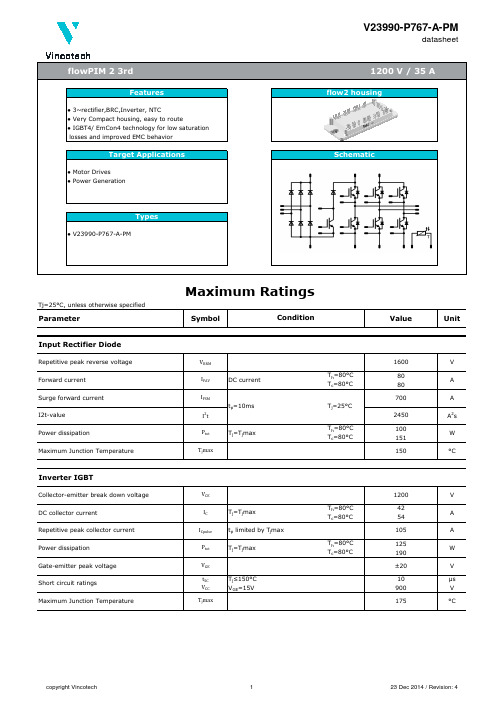
Brake IGBT
Collector-emitter break down voltage DC collector current Repetitive peak collector current Power dissipation Gate-emitter peak voltage Short circuit ratings Maximum Junction Temperature VCE IC ICpuls Ptot VGE tSC VCC Tjmax Tj≤150°C VGE=15V Tj=Tjmax tp limited by Tjmax Tj=Tjmax Th=80°C Tc=80°C Th=80°C Tc=80°C 1200 35 40 75 112 170 ±20 10 900 175 V A A W V µs V °C
Unit
Inverter FWD
Peak Repetitive Reverse Voltage DC forward current Repetitive peak forward current Power dissipation Maximum Junction Temperature VRRM IF IFRM Ptot Tjmax Tj=Tjmax tp limited by Tjmax Tj=Tjmax Th=80°C Tc=80°C Th=80°C Tc=80°C 1200 50 65 75 100 151 175 V A A W °C
Inverter IGBT
Collector-emitter break down voltage DC collector current Repetitive peak collector current Power dissipation Gate-emitter peak voltage Short circuit ratings Maximum Junction Temperature VCE IC ICpulse Ptot VGE tSC VCC Tjmax Tj≤150°C VGE=15V Tj=Tjmax tp limited by Tjmax Tj=Tjmax Th=80°C Tc=80°C Th=80°C Tc=80°C 1200 42 54 105 125 190 ±20 10 900 175 V A A W V µs V °C
FOSAN富信电子 二极管 TB05S-TB10S-产品规格书

安徽富信半导体科技有限公司ANHUI FOSAN SEMICONDUCTOR TECHNOLOGY CO.,LTD.TB05S-TB10SBridge Rectifier Diode 整流桥■Features 特点Glass passivated chip junction 玻璃钝化结High surge current capability 高浪涌电流能力Reflow Solder Temperature 220℃回流焊温度220度Package 封装:TBS■Maximum Rating 最大额定值(T A =25℃unless otherwise noted 如无特殊说明,温度为25℃)Characteristic 特性参数Symbol 符号TB05S TB1S TB2S TB4S TB6S TB8S TB10S Unit 单位Peak Reverse Voltage 反向峰值电压V RRM 501002004006008001000V DC Reverse Voltage 直流反向电压V R(DC)501002004006008001000V RMS Reverse Voltage 反向电压均方根值V R(RMS)3570140280420560700V Forward Rectified Current 正向整流电流I F 1A Peak Surge Current 峰值浪涌电流I FSM 30A Thermal Resistance J-A 结到环境热阻R θJA 75℃/WJunction and Storage Temperature 结温和储藏温度T J ,T stg150℃,-55to+150℃■Electrical Characteristics 电特性(T A =25℃unless otherwise noted 如无特殊说明,温度为25℃)Characteristic 特性参数Symbol 符号Min 最小值Typ 典型值Max 最大值Unit 单位Condition 条件Forward Voltage 正向电压降V F 1V I F =0.4A Reverse Current (T A =25℃)反向漏电流(T A =125℃)I R 5500uA V R =V RRM Diode Capacitance 二极管电容C D10pFV R =4V,f=1MHz安徽富信半导体科技有限公司ANHUI FOSAN SEMICONDUCTOR TECHNOLOGY CO.,LTD.TB05S-TB10S ■Typical Characteristic Curve典型特性曲线Figure1:Forward Current Derating Curve Figure2:Peak Forward Surge CurrentFigure3:Instantaneous Forward Characteristics Figure4:Reverse Leakage Characteristics■Dimension外形封装尺寸TBS Dimensions in inches and(millimeters)。
- 1、下载文档前请自行甄别文档内容的完整性,平台不提供额外的编辑、内容补充、找答案等附加服务。
- 2、"仅部分预览"的文档,不可在线预览部分如存在完整性等问题,可反馈申请退款(可完整预览的文档不适用该条件!)。
- 3、如文档侵犯您的权益,请联系客服反馈,我们会尽快为您处理(人工客服工作时间:9:00-18:30)。
天津中环半导体股份有限公司
TIANJIN ZHONGHUAN SEMICONDUCTOR CO.,LTD.
T20XB(20~80)
橋式整流器Bridge Rectifier
■特徵 Features ■外形尺寸和印記 Outline Dimensions and Mark
● I o
20A 單位Unit :mm ● V RRM 200V~800V
● 玻璃鈍化芯片 Glass passivated chip ● 耐正向浪湧電流能力高
■用途 Applications
● 作一般電源單相橋式整流用 rectifier applications
■極限值(絕對最大額定值) Limiting Values (Absolute Maximum Rating )
T20XB
參數名稱
Item
符號 Symbol 單位Unit
條件 Conditions
20 40
60
80
貯存溫度
Storage Temperature T stg ℃ -40 ~+150 结温
Junction Temperature T j ℃
+150
反向重復峰值電壓
Repetitive Peak Reverse Voltage V RRM
V 200 400600800
用散熱片 T c =87℃
With heatsink T c =87℃
20 平均整流輸出電流
Average Rectified Output Current I o A
50H z 正弦波,電阻負載50H Z sine wave, R-load 無散熱片 T a =25℃
Without heatsink T a =25℃
3.5 正向(不重復)浪涌電流
Surge(Non-repetitive)Forward Current I FSM A
50H Z 正弦波,一個周期,T a =25℃
50H Z sine wave, 1 cycle, T a =25℃ 240 绝缘耐压
Dielectric Strength Vdis kV
端子與外殼之間外加交流電,一分鐘
Terminals to case ,AC 1 minute
2.5 安装扭矩
Mounting Torque
TOR kg ·cm
推荐值:5kg ·cm
Recommend torque :5kg ·cm
8
■電特性 (T a =25℃ 除非另有規定) Electrical Characteristics (T a =25℃ Unless otherwise specified )
參數名稱 Item 符號 Symbol 單位 Unit 測試條件 Test Condition
最大值
Max
正向峰值電壓
Peak Forward Voltage V FM V
I FM =10A, 脈衝測試,單個二極管的額定值
I FM =10A, Pulse measurement, Rating of per diode
1.1 反向峰值電流
Peak Reverse Current
I RRM
μA V RM =V RRM ,脈衝測試,單個二極管的額定值
V RM =V RRM , Pulse measurement, Rating of per diode
10 R θJ-A 結和環境之間,無散熱片
Between junction and ambient, Without heatsink
22 R θJ-L 結和引線之間,無散熱片
Between junction and lead, Without heatsink
5 熱阻
Thermal Resistance
R θJ-C ℃/W 結和管殼之間,用散熱片
Between junction and case, With heatsink
1.5
2.2±0.2
T20XB60 05304.0±0.2
17.5±0.5
10±0.2
7.5±0.27.5±0.2
5
20±0.3
+0.1588。