ZXGD3003E6中文资料(Zetex Semiconductors)中文数据手册「EasyDatasheet - 矽搜」
ZXMN3B01FTA中文资料(Zetex Semiconductors)中文数据手册「EasyDatasheet - 矽搜」
VDD =15V, I D =2.5A RG =6.0Ω, V GS =10V VDS =15V,V GS =5V, I =2.5A VDS =15V,V GS =10V, I =2.5A
二极管正向电压(1) 反向恢复时间(3) 反向恢复电荷(3)
TJ =25°C, I S=1.7A, VGS =0V TJ =25°C, I F=2.5A, di/dt= 100A/µs
器件标识
WIDTH 8mm 8mm
数量 每卷
3000单位 10000台
4
3Leabharlann 213mm x 2mm Dual MLP underside view
DNB
第 1期
- 2005年 10月 1
芯片中文手册,看全文,戳
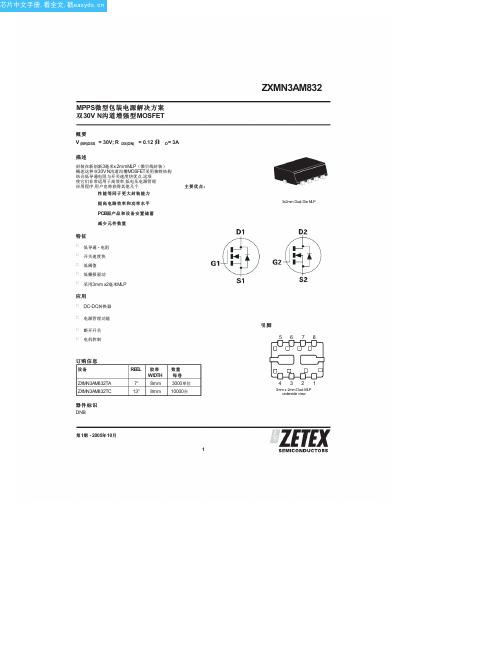
ZXMN3AM832
绝对最大额定值 .
参数 漏源电压 栅源电压 连续漏电流用V 符号
热阻
参数 结到环境(一)(F) 结到环境(B)(F) 结到环境(C)(F) 结到环境(D)(F) 结到环境(D)(G) 结到环境(E )(G) 符号 值 单元
R JA R JA R JA R JA R JA R JA
83.3 51 125 111 73.5 41.7
°C/W °C/W °C/W °C/W °C/W °C/W
芯片中文手册,看全文,戳
ZXMN3AM832
MPPS微型包装电源解决方案 双 30V N沟道增强型 MOSFET
概要
V (BR)DSS = 30V; R
描述
DS(ON)
= 0.12 ; I
D=
3A
封装在新创新3毫米x 2mmMLP(微引线封装) 概述这种双30V N沟道沟槽MOSFET采用独特结构 结合低导通电阻与开关速度快优点.这项 使它们非常适用于高效率,低电压电源管理 应用程序.用户也将获得其他几个 性能等同于更大封装能力 提高电路效率和功率水平
炜煌 E36 快速安装手册说明书
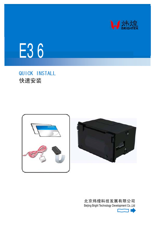
QUICK INSTALL 快速安装 北京炜煌科技发展有限公司Beijing Bright Technology Development Co.,Ltd●打印机各部件一览 Printer Parts Names1.纸仓盖 Paper Case Cover2.指示灯/LF 键 Indicator Light/LF Button3.纸轴 Paper Roller4.纸挡板 accessory5.纸卷 Paper Roll6.色带 Ribbon7.螺钉 Screw8.通讯接口 Interface Connector9.电源Power Connector 10.固定架 Holder按钮开关的操作及指示灯打印机上电后指示灯保持常亮状态,打印机缺纸时指示灯闪,不能接受数据。
正常上电后,LF 键为走纸键。
自检测方式打印机断电,按LF 键不放手同时给打印机上电,打印机就会打印出自检条。
Operation SpecificationAfter turning on the printer, the indicator light will keep on. When the light flash, it shows that the paper is lacking, and the printer can not receive data.Press the LF button, the printer will feed paper.The Self TestPress the LF button, do not release and turn on the printer at the same time,and then the printer will print out the self-check scrip.●尺寸 SizeWH-E36型尺寸 Product Size:外型尺寸 Outline Dimension:机型Model 外形尺寸E36 串/并接口 107.4mm X 61.4mm X 71.8mmE36 485/422接口 107.4mm X 61.4mm X 84.5mm安装尺寸Mounting Dimension:机型Model L1 L2 E36 串/并接口 63.8mm 71.8mm E36 485/422接口 76.7mm 84.5mm嵌入深度 Inlaid Deepness:机型Model 嵌入深度E36 串/并接口 63.8mmE36 485/422接口 76.7mm●安装 Installation安装方法:把打印机嵌入部分插入仪器或设备面板的安装孔内,再打开纸仓盖把螺钉拧紧,塑料卡子随着螺钉的拧紧顶在设备面板后面,左右对称各一套,安装方法相同。
ZETEX ZXGD3003E6 5A(peak) gate driver in SOT23-6

ZXGD3003E65A(peak) gate driver in SOT23-6General descriptionThe ZXGD3003E6 is a high-speed non-inverting single MOSFET gate driver capable of driving up to 5A into a MOSFET or IGBT gate capacitive load from supply voltages up to 40V. With typical propagation delay times down to 2ns and rise/fall times down to 9ns this device ensures rapid switching of the power MOSFET or IGBT to minimize power losses and distortion in high current fast switching applications.The ZXGD3003E6 is inherently rugged to latch-up and shoot-through, and its wide supply voltage range allows full enhancement to minimize on-losses of the power MOSFET or IGBT.Its low input voltage requirement and high current gain allows high current driving from low voltage controller ICs, and the optimized pin-out SOT23-6 package with separate source and sink pins eases board layout, enabling reduced parasitic inductance and independent control of rise and fall slew rates. Features Array•40V operating voltage range• 5 amps peak output current•Fast switching emitter-follower configuration•2ns propagation delay time•19ns rise/fall time, 1000pF load•Low input current requirement• 1.6A(source)/1.4A(sink) output current from 10mA input•SOT23-6 package•Separate source and sink outputs for independent control of rise and fall time•Optimized pin-out to ease board layout and minimize trace inductance•No Latch Up•No shoot through•Near - Zero quiescent and output leakage currentTypical application circuitApplicationsPower MOSFET and IGBT Gate Driving in •Synchronous switch-mode power supplies •Secondary side synchronous rectification •Plasma Display Panel power modules •1, 2 and 3-phase motor control circuits•Audio switching amplifier power output stagesPin configurationPin descriptionOrdering informationDevice marking3003Pin Name Pin Function V CC Driver supplyIN 1 / IN 2Driver input pins. These are normally connected together by circuit tracks. GND GroundSOURCE Source current output.SINKSink current output.DeviceReel size (inches)Tape width (mm)Quantity perreelZXGD3003E6TA78 embossed3000Absolute maximum ratingsParameter Symbol Limit Unit Supply voltage V CC40V Input voltage V IN40V Peak sink current(c)I(sink)PK5A Source current @ I IN1 + I IN2 =10mA(a)I(source) 1.6A Sink current @ I IN1 + I IN2 =10mA(a)I(sink) 1.4A Input current(c)I IN1, I IN21A Power dissipation at T A =25°C(a)(b)P D 1.1W Linear derating factor8.8mW/°C Operating and storage temperature range T j, T stg-55 to +150°CThermal resistanceParameter Symbol Value Unit Junction to ambient(a)(b)R⍜JC113°C/W NOTES:(a)For a device surface mounted on 25mm x 25mm x 0.6mm FR4 PCB with high coverage of single sided 1oz copper,in still air conditions.(b)For device with two active dice running at equal power.(c)Pulse width <=300us limit repetition rate to comply with maximum junction temperature.Electrical characteristics (at Tamb = 25°C unless otherwise stated).Switching time test circuits Timing diagramParameterSymbol Min.Typ.Max.Unit Conditions Output voltage, high V OH V CC – 0.4V I source = 1A Output voltage, lowV OL0.4V I sink = 1A Source output leakage currentI L(source)1A V CC = 40V,V IN1 = V IN2 = 0V Sink output leakage currentI L(sink)1A V CC = 40V,V IN1 = V IN2 = V CC Quiescent currentI Q20nA V CC = 32V,V IN1 = V IN2 = 0V Source output current I (source)1 1.6A I IN1+I IN2 = 10mA Sink output currentI (sink)11.4A I IN1+I IN2 = 10mA Source output current I (source)PK 5A I IN1+I IN2 = 500mA Sink output current I (sink)PK 5A I IN1+I IN2 = 500mA Gate driverswitching timest d(rise)t rt d(fall)t f 1.88.91.78.9ns ns ns ns C L =1nF , R L =1⍀,V CC =12V, V IN =10V,R S =25⍀Gate driverswitching timest d(rise)t rt d(fall)t f477485ns ns ns nsC L =1nF , R L =1⍀,V CC =12V, V IN =10V,R S =1k ⍀Typical gate driver characteristicsSOT23-6 Package outlineNote: Controlling dimensions are in millimeters. Approximate dimensions are provided in inchesDIM MillimetersInchesMin.Max.Min.Max.A 0.90 1.450.03540.0570A10.000.150.000.0059A20.90 1.300.03540.0511b 0.350.500.00780.0196C 0.090.260.00350.0102D 2.70 3.100.10620.1220E 2.20 3.200.08660.1181E1 1.30 1.800.05110.0708L 0.100.600.00390.0236e 0.95 REF 0.0374 REF e1 1.90 REF 0.0748 REF L0°30°0°30°Zetex sales offices EuropeZetex GmbHKustermann-park Balanstraße 59D-81541 München GermanyTelefon: (49) 89 45 49 49 0Fax: (49) 89 45 49 49 49**********************AmericasZetex Inc700 Veterans Memorial Highway Hauppauge, NY 11788USATelephone: (1) 631 360 2222Fax: (1) 631 360 8222*******************Asia PacificZetex (Asia Ltd)3701-04 Metroplaza Tower 1Hing Fong Road, Kwai Fong Hong KongTelephone: (852) 26100 611Fax: (852) 24250 494********************Corporate HeadquartersZetex Semiconductors plcZetex Technology Park, Chadderton Oldham, OL9 9LL United KingdomTelephone: (44) 161 622 4444Fax: (44) 161 622 4446************© 2007 Published by Zetex Semiconductors plcDefinitionsProduct changeZetex Semiconductors reserves the right to alter, without notice, specifications, design, price or conditions of supply of any product or service. Customers are solely responsible for obtaining the latest relevant information before placing orders.Applications disclaimerThe circuits in this design/application note are offered as design ideas. It is the responsibility of the user to ensure that the circuit is fit for the user’s application and meets with the user’s requirements. No representation or warranty is given and no liability whatsoever is assumed by Zetex with respect to the accuracy or use of such information, or infringement of patents or other intellectual property rights arising from such use or otherwise. Zetex does not assume any legal responsibility or will not be held legally liable (whether in contract,tort (including negligence), breach of statutory duty, restriction or otherwise) for any damages, loss of profit, business, contract,opportunity or consequential loss in the use of these circuit applications, under any circumstances.Life supportZetex products are specifically not authorized for use as critical components in life support devices or systems without the express written approval of the Chief Executive Officer of Zetex Semiconductors plc. As used herein:A. Life support devices or systems are devices or systems which:1.are intended to implant into the body or2.support or sustain life and whose failure to perform when properly used in accordance with instructions for use provided in the labeling can be reasonably expected to result in significant injury to the user.B. A critical component is any component in a life support device or system whose failure to perform can be reasonably expected tocause the failure of the life support device or to affect its safety or effectiveness.ReproductionThe product specifications contained in this publication are issued to provide outline information only which (unless agreed by the company in writing) may not be used, applied or reproduced for any purpose or form part of any order or contract or be regarded as a representation relating to the products or services concerned. Terms and ConditionsAll products are sold subjects to Zetex’ terms and conditions of sale, and this disclaimer (save in the event of a conflict between the two when the terms of the contract shall prevail) according to region, supplied at the time of order acknowledgement.For the latest information on technology, delivery terms and conditions and prices, please contact your nearest Zetex sales office.Quality of productZetex is an ISO 9001 and TS16949 certified semiconductor manufacturer.To ensure quality of service and products we strongly advise the purchase of parts directly from Zetex Semiconductors or one of our regionally authorized distributors. For a complete listing of authorized distributors please visit: /salesnetworkZetex Semiconductors does not warrant or accept any liability whatsoever in respect of any parts purchased through unauthorized sales channels.ESD (Electrostatic discharge)Semiconductor devices are susceptible to damage by ESD. Suitable precautions should be taken when handling and transporting devices.The possible damage to devices depends on the circumstances of the handling and transporting, and the nature of the device. The extent of damage can vary from immediate functional or parametric malfunction to degradation of function or performance in use over time.Devices suspected of being affected should be replaced.Green complianceZetex Semiconductors is committed to environmental excellence in all aspects of its operations which includes meeting or exceeding reg-ulatory requirements with respect to the use of hazardous substances. Numerous successful programs have been implemented to reduce the use of hazardous substances and/or emissions.All Zetex components are compliant with the RoHS directive, and through this it is supporting its customers in their compliance with WEEE and ELV directives.Product status key:“Preview”Future device intended for production at some point. Samples may be available “Active”Product status recommended for new designs “Last time buy (LTB)”Device will be discontinued and last time buy period and delivery is in effect “Not recommended for new designs”Device is still in production to support existing designs and production “Obsolete”Production has been discontinued Datasheet status key:“Draft version”This term denotes a very early datasheet version and contains highly provisional information, whichmay change in any manner without notice.“Provisional version”This term denotes a pre-release datasheet. It provides a clear indication of anticipated performance.However, changes to the test conditions and specifications may occur, at any time and without notice.“ssue”This term denotes an issued datasheet containing finalized specifications. However, changes tospecifications may occur, at any time and without notice.。
ZMV832ATA中文资料(Zetex Semiconductors)中文数据手册「EasyDatasheet - 矽搜」

SOT23 SOD523
830系列
SOT323 SOD323
*Where steeper CVslopes are required there is the 12Vhyperabrupt range. ZC930,ZMV930,ZV930,ZV931系 列
CD AE
CE AF
CF
AG
CG
ZMV8Z2M9VA8ZT2MA9VB8ZT3MA0VA8ZT3MA0VB8ZT3MA1VA8ZT3MA1VB8ZT3MA2VA8ZT3MA2VB8ZT3MA3VA8ZT3MA3VB8ZT3MA4VA8ZT3MA4VB8ZT3MA5VA8T3A5BTA
订货代码
带尺寸
7英寸13(英1寸80(毫3米30)毫米)
第 8期 - 2005年 3月 1
SEMICONDUCTORS
芯片中文手册,看全文,戳
830系列
调谐特性在环境温度 Tamb = 25°C
部分
电容( pF)
V R=2V, f=1MHz
MIN.
NOM.
MAX.
829A
7.38
8.2
9.02
829B
7.79
8.2
8.61
830A
9.0
SOT23
部 分马 克 订货代码
C2A C5A ZDC833AZTDAC834ATA
300010000
数量每卷
SOD523 订购代码和部件标记
SOD323
ZXCD1000中文资料(Zetex Semiconductors)中文数据手册「EasyDatasheet - 矽搜」

引脚名称
音频A
三角形 振荡器一
Dist Cosc OSC乙
三角乙 音频乙
Gnd 输出B Gnd2 9VB VCC 9VA 输出A 5V5
引脚说明
音频输入通道A 三角输入通道A
三角形输出 无连接 外部定时电容节点(设置开关频率)
三角形输出(从机ZXCD1000立体声应用) 三角输入通道B 音频输入通道B 小信号GND 通道B PWM输出驱动外部MOSFET桥梁 电力GND(输出驱动器) 内部电源轨(与去耦1μF帽) 电源输入端(最大值= 18V) 内部电源轨(与去耦1μF上限). 通道PWM输出驱动外部MOSFET桥梁 内部电源轨(与去耦1μF帽)
类似地,随着AudioA / B信号下降时,占空比 周期也相应地降低.因此,音频输入 脉冲宽度调制比较器输出.这项 原理如图3a,B,c和d.该 比较器输出进行缓冲,并用于驱动 OUTA和OUTB输出.反过来,这些驱动扬声器 负荷(与包含在PWM中音频信息
信号)通过片外桥式输出和单级
L-C滤波器网络.
(OUT A / B上升/下降)
内部铁路公差 内部铁路公差 输入阻抗 输入阻抗
偏置电平 偏置电平
振幅
条件
VCC = 12V VCC = 18V, 16V Cosc = 330pF Cosc = 330pF
空载 空载 负载电容
= 2200pF 1μF解耦 1μF解耦
极限
MIN TYP
12
16
150
200
芯片中文手册,看全文,戳
高 防 护 真 D类 音 频 放 大 器 解 决 方 案
ZXCD1000
描述
该ZXCD1000提供完整控制和调制功能以高效 率高性能D类开关音频放大器解决方案心脏.在与 ZetexHDMOS MOSFET器件相结合,ZXCD1000提供高性能 音频放大器,D类所有固有优势
三星AMOLED驱动芯片中文版说明书
表 5 所示为其他端口。 Symbol I/O 功能描述 DUMMYR[3:1] 电阻测量管脚,正常情况下悬空。 DUMMYL[3:1] DUMMY 无用管脚,悬空即可。 V0/V63 O 伽玛电压镜像管脚。 VDD3DUM O 内部与 VDD3 接在一起。
VSSDUM FUSE_EN RTEST EN_EXCLK EN_CLK TEST_MODE[1:0] TEST_IN[6:0] TE TEST_OUT[2:0]
表 2 系统接口
表3为 Symbol MDP MDN MSP MSN GPIO[9:0] (DB[17:8]) S_CSB(DB [7])
MDDI 管脚作用。 I/O 功能描述 I/O MDDI 数据输入/输出正端,如果 MDDI 不用,该端口悬空。 I/O MDDI 数据输入/输出负端,如果 MDDI 不用,该端口悬空。 I MDDI 数据选通输入正端,如果 MDDI 不用,该端口悬空。 I MDDI 数据选通输入负端,如果 MDDI 不用,该端口悬空。 I/O 总体输入输出,如果在 MDDI 中没有用 GPIO 的话,这些管 脚应该置地。 O 子屏幕驱动 IC 片选信号。 低电平时说明子屏幕驱动 IC 可用,高电平时说明子屏幕驱动
表 1 电源接口
如表 2 所示为系统接口。 Symbol I/O 功能描述 S_PB I 选择 CPU 接口模式,低电平时为并行接口,高电平时为串行 接口。 MDDI_E I 选择 MDDI 接口,低电平时 MDDI 接口不可用,高电平时 N MDDI 接口可用。 ID_MIB I 选择 CPU 种类, 低电平为 intel 80 系列 CPU, 高电平为 motorola 68 系列 CPU,如果 S_PB 是高电平,该端口为 ID 设置端口。 CSB I 片选信号,低电平芯片可用,高电平芯片不可用。 RS I 寄存器选择管脚。 低电平时,指令/状态,高电平时为指令参数/RAM 数据。 不用时需与 VDD3 接在一起。 RW_WR I 管脚作用 CPU 种类 管脚说明 B/SCL RW 68 系列 读写选择,低电平写,高电平读。 WRB 80 系列 写选通作用,在上升沿捕获数据。 SCL 串行接口 时钟同步信号。 E_RDB I 管脚作用 CPU 种类 管脚说明 E 68 系列 读写操作使能端。 RDB 80 系列 读选通作用,低电平时读出数据。 选择串行模式时,将此端口接在 VDD3 上。 SDI I 串行接口的数据输入接口,在 SCL 上升沿捕捉到输入数据,
全系列场效应管VMOSIGBT参数

全系列场效应管VMOSIGBT参数场效应管(FET)和绝缘栅双极晶体管(IGBT)是两种常见的功率开关器件,在电子和电力系统中广泛应用。
在了解这两种器件的参数之前,我们先来了解一下它们的基本工作原理。
场效应管(FET)是一种控制電荷流通的三端器件。
主要由源极、漏极和栅极组成。
FET的特点是输入电流较小,输出电阻较低,能够承受较大的功率。
FET的主要类型有MOSFET(金属氧化物半导体场效应管)和VMOS(垂直型金属氧化物半导体场效应管)。
VMOS是一种特殊类型的MOSFET。
VMOS的结构使其能够承受较高的功率。
其主要特点是漏极电流和栅极电流之比较低,可以实现高转导,从而具有较小的输入电容和较高的开关速度。
由于VMOS的漏极电流较低,可以减少功耗和发热,提高效率,并且可以减少开关损耗。
IGBT是一种双极晶体管,结合了场效应管和双极晶体管的优点。
它具有高输入阻抗和低输出电阻的特点。
IGBT的主要工作原理是栅极电压控制电流流动,从而实现开关功能。
它广泛应用于高效率、高频率和高电压的功率应用领域,例如电动车、工业电机控制和电力变换等。
现在,让我们来看一下VMOS和IGBT的一些重要参数:1.最大工作电压(VDS/VCE):这是器件可以承受的最大电压。
一旦超过这个电压,器件可能会发生击穿或损坏。
2.最大电流(ID/IC):这是器件可以承受的最大电流。
如果超过这个电流,可能会导致器件过热或损坏。
3. 导通电阻(RDS(on)/RCE(on)):这是器件在导通状态下的电阻。
较低的导通电阻可以减小功耗和电压降。
4.开启时间(tON)和关闭时间(tOFF):这是器件从关断状态到导通状态和从导通状态到关断状态的转换时间。
较短的开启和关闭时间可以提高开关速度和效率。
5. 输入电容(Ciss)和输出电容(Coss):这是器件的输入和输出电容。
较小的电容可以减小开关损耗和功耗。
6.热阻(θJA/θJC):这是器件的热阻,描述了器件散热的能力。
维沙耶芯片电阻说明书
Document Number: 28744For technical questions, contact: *************************** MCS 0402 VG01, MCT 0603 VG01, MCU 0805 VG01 andMCA 1206 VG01 thin film flat chip resistors with establishedreliability are the perfect choice for all high-reliabilityapplications typically found in military, aircraft and spacecraftelectronics. These versions supplement the families ofprofessional and precision thin film flat chip resistorsMCS 0402, MCT 0603, MCU 0805 and MCA 1206.∙Established reliability, failure rate level E6∙Advanced thin film technology ∙Pure Sn termination on Ni barrier layer ∙Single lot date code ∙Material categorization: For definitions of complianceplease see /doc?99912APPLICATIONS∙Military ∙Avionics ∙Space Notes•These resistors do not feature a limited lifetime when operated within the permissible limits. However, resistance value drift increasing over operating time may result in exceeding a limit acceptable to the specific application, thereby establishing a functional lifetime.•The failure rate level E6 (10-6/h, πQ = 0.3), corresponding to MIL Level P, is superior to level E5 (10-5/h, πQ = 1) and thus may be used as areplacement.METRIC SIZE IMPERIAL0402060308051206EN/CECC RR1005M RR1608M RR2012M RR3216M TECHNICAL SPECIFICATIONSDESCRIPTIONMCS 0402 VG01MCT 0603 VG01MCU 0805 VG01MCA 1206 VG01EN/CECC style (size)RR1005M RR1608M RR2012M RR3216MResistance range10 Ωto 1 M Ω; 0Ω 1 Ωto 1 M Ω; 0ΩResistance tolerance± 1 %; ± 0.1 %T emperature coefficient± 50ppm/K; ± 15 ppm/K Rated dissipation, P 700.063W 0.1W 0.125W 0.25W Operating voltage, U max. AC/DC50V 75 V 150V 200V Permissible film temperature, ϑF max.125︒C Operating temperature range- 55 °C to 125 °C Max. resistance change at P 70for resistance range, |∆R /R| max. after:10 Ωto 1 M Ω 1 Ωto 1 M Ω1000h≤ 0.25 %8000h≤ 0.5 %225000h≤ 1.5 %Permissible voltage against ambient(insulation):1 min; U ins75V 100V 200V 300V Continuous75V 75V 75V 75V Assessed failure rate levelE6 = 10-6/h Quality factor, πQ0.3Failure rate: FIT observed < 0.1 x 10⁻⁹/h For technical questions, contact: ***************************Document Number: 28744Notes•The products can be ordered using either the PART NUMBER or the PRODUCT DESCRIPTION.•Products within a packaging unit are single lot date code.TYPE/SIZEVERSION TCR RESISTANCE TOLERANCE PACKAGING MCS 0402MCT 0603MCU 0805MCA 1206H = EN 140401-801,“Version E”;failure rate level E6 C = ± 50 ppm/K E = ± 15 ppm/K Z = Jumper 3 digit value 1 digit multiplier MULTIPLIER8 = *10-29 = *10-10 = *1001 = *1012 = *1023 = *1034 = *1040000 = Jumper F = ± 1 %B = ± 0.1 %Z = JumperE1E0P1P5Product Description: MCT 0603-50 1% VG01 P5 287KProduct Description: MCT 0603 VG01 P5 0R0MCT 0603-50 1 %VG01P5287K MCT 0603--VG01P50R0TYPE/SIZETCR T OLERANCE VERSION PACKAGING RESISTANCE MCS 0402MCT 0603MCU 0805MCA 1206± 50 ppm/K ± 15 ppm/K ± 1 %± 0.1 %VG01 = EN 140401-801,“Version E”;failure rate level E6E1E0P1P549R9 = 49.9 Ω287K = 287 k Ω0R0 = JumperMC T 0603H Z 0000Z P 50006032873500Document Number: 28744For technical questions, contact: *************************** Note•The ordering information according to EN 140401-801:2007 shown above succeeds and replaces the ordering information according to earlier versions of the detail specification EN 140401-801 or its predecessor CECC 40401-801, for example:CECC 40401-801 EZ RR1608M C 287K F E6CECC 40401-801 S RR1608M C 287K F E6with EZ; S Assessment level, where EZ is successor to and superior replacement for SRR1608M Style, with suffix M for “metric”C Temperature coefficient, according to the detail specificationC = ± 50 ppm/K; E = ± 15 ppm/K Note•According to EN 140401-801, resistance values are to be selected from the E96 series for ±1% tolerance and from the E192 series for ±0.1 % tolerance.EN140401-801EZRR1608M-0R00-E6The elements used in the component number have the following meaning:EN140401-801EZRR1608MR287KF E6EN detail specification number Assessment level for the zero-defect approach Style (size)T emperature coefficient, according to EN 60062R = ± 50 ppm/K; P = ± 15 ppm/K Resistance, according to EN 60062, 4 characters T olerance on rated resistance, according to EN 60062F = ± 1 %; B = ± 0.1 %Failure rate level according to EN 60115-1, annex ZRTEMPERATURE COEFFICIENT AND RESISTANCE RANGEDESCRIPTIONRESISTANCE TCRTOLERANCE MCS 0402 VG01MCT 0603 VG01MCU 0805 VG01MCA 1206 VG01± 50 ppm/K± 1 %10 Ωto 1 M Ω 1 Ωto 1 M Ω1Ωto 1 M Ω1Ωto 1 M Ω± 15 ppm/K± 0.1 %100Ωto 33.2 k Ω100Ωto 47.5 k Ω100Ωto 100k Ω43.2Ωto 332k ΩJumper ≤ 20m Ω; I max. = 0.63 A ≤ 20m Ω; I max. = 1 A ≤ 20m Ω; I max. = 1.5 A≤ 20m Ω; I max. = 2 A PACKAGINGTYPECODE QUANTITY CARRIER TAPE WIDTH PITCH REEL DIAMETER MCS 0402 VG01E11000Paper tape acc. IEC 60286-3T ype I 8 mm 2 mm 180 mm/7"E010 000MCT 0603 VG01P110008 mm 4 mm P55000MCU 0805 VG01P11000P55000MCA 1206 VG01P11000P55000 For technical questions, contact: ***************************Document Number: 28744Note•Resistors MCA 1206 VG01 and MCU 0805 VG01 are marked using to the four-character code system of IEC 60062, 4.2.3.Resistors MCT 0603 VG01 and MCS 0402 VG01 do not show any marking on their light blue protective coating.Note•The given solder pad dimensions reflect the considerations for board design and assembly as outlined e.g. in standards IEC 61188-5-x, or in publication IPC 7351. They do not guarantee any supposed thermal properties, however, they will be found adequate for most general applications.DIMENSIONS AND MASSTYPEH (mm)L (mm)W (mm)W T (mm)T b (mm)T t (mm)MASS (mg)MCS 0402 VG010.32 ± 0.05 1.0 ± 0.050.5 ± 0.05> 75 % of W 0.2 ± 0.10.2 + 0.1/- 0.150.6MCT 0603 VG010.45 + 0.1/- 0.05 1.55 ± 0.050.85 ± 0.10.3 + 0.15/- 0.21.9MCU 0805 VG010.45 + 0.1/- 0.052.0 ± 0.11.25 ± 0.150.4 + 0.1/- 0.2 4.6MCA 1206 VG010.55 ± 0.1 3.2 + 0.1/- 0.2 1.6 ± 0.150.5 ± 0.259.2RECOMMENDED SOLDER PAD DIMENSIONSTYPE WAVE SOLDERINGREFLOW SOLDERING G(mm)Y (mm)X (mm)Z (mm)G (mm)Y (mm)X (mm)Z(mm)MCS 0402 VG01----0.350.550.55 1.45MCT 0603 VG010.551.10 1.102.750.650.700.95 2.05MCU 0805 VG010.801.25 1.50 3.300.900.90 1.402.70MCA 1206 VG011.40 1.50 1.90 4.40 1.50 1.15 1.753.80grade ceramic (Al2O3) substrate and conditioned to achieve the desired temperature coefficient. Specially designed inner contacts are deposited on both sides. A special laser is used to achieve the target value by smoothly cutting a meander groove in the resistive layer without damaging the ceramics. For the high ohmic range, optimized cermet products provide comparable properties. The resistor elements are covered by a protective coating designed for electrical, mechanical and climatic protection. The terminations receive a final pure tin on nickel plating.The result of the determined production is verified by an extensive testing procedure performed on 100 % of the individual resistors. This includes pulse load screening for the elimination of products with a potential risk of early life failures according to EN 140401-801, 2.1.2.2 (feasible for R≥ 10 Ω). Only accepted products are laid directly into the paper tape in accordance with EN 60286-3 (3), Type I.Products within a packaging unit are from the same production lot and carry the same date code.ASSEMBLYThe resistors are suitable for processing on automatic SMD assembly systems. They are suitable for automatic soldering using wave, reflow or vapour phase as shown in IEC61760-1 (3). Solderability is specified for 2 years after production or requalification. The permitted storage time is 20 years.The resistors are RoHS compliant; the pure tin plating provides compatibility with lead (Pb)-free soldering processes. The immunity of the plating against tin whisker growth has been proven under extensive testing.The encapsulation is resistant to all cleaning solvents commonly used in the electronics industry, including alcohols, esters and aqueous solutions. The suitability of conformal coatings, if applied, shall be qualified by appropriate means to ensure the long-term stability of the whole system.∙2000/53/EC End of Vehicle life Directive (ELV) and Annex II (ELV II)∙2011/65/EU Restriction of the use of Hazardous Substances directive (RoHS)∙2002/96/EC Waste Electrical and Electronic Equipment Directive (WEEE)APPROVALSThe resistors are approved within the IECQ-CECC Quality Assessment System for Electronic Components to the detail specification EN140401-801 which refers to EN60115-1, EN140400 and the variety of environmental test procedures of the IEC 60068 (3)series.Conformity is attested by the use of the CECC logo () as the mark of conformity on the package label.Vishay BEYS C HLAG has achieved “Approval of Manufacturer” in accordance with IEC QC001002-3, clause 2. The release certificate for “Technology Approval Schedule” in accordance with CECC240001 based on IEC QC001002-3, clause 6 is granted for the Vishay BEYSCHLAG manufacturing process.The Vishay BEYSC HLAG production facility is registered with the CAGE code D9539.RELATED PRODUCTSA wider range of TCR, tolerance and resistance values, plus the option of values from a different E series is available with products approved to EN 140401-801, Version A, without established reliability, nominal failure rate level E0 (quality factor πQ = 3). See the datasheets:∙“Professional Flat Chip Resistors”(/doc?28705)∙“Precision Flat Chip Resistors”(/doc?28700)Notes(1)Global Automotive Declarable Substance List, see .(2)CEFIC (European Chemical Industry Council), EECA (European Electronic Component Manufacturers Association), EICTA (European tradeorganisation representing the information and communications technology and consumer electronics), see /index.php?id=1053&id_article=340.(3)The quoted IEC standards are also released as EN standards with the same number and identical contents.Document Number: 28744For technical questions, contact: *************************** For technical questions, contact: ***************************Document Number: 28744Document Number: 28744For technical questions, contact: *************************** •“Precision Flat Chip Resistors”, document no. 28700EN 140400, sectional specificationEN 140401-801, detail specificationFor further information on the tests and requirements ofthese products please refer to the specifications mentionedabove, and to the following datasheets:•“Professional Flat Chip Resistors”(/doc?28705)•“Precision Flat Chip Resistors”(/doc?28700)HISTORICAL 12NC INFORMATION∙The resistors had a 12-digit code starting with 2312∙The subsequent 4 digits indicated the resistor type,specification and packaging; see the 12NC table∙The remaining 4digits indicate the resistance value:-The first 3digits indicated the resistance value-The last digit indicated the resistance decade inaccordance with the resistance decade table RESISTANCE DECADE Historical 12NC ExampleThe 12NC of a MC T 0603 VG01 resistor, value 287K andTCR 50 with ± 1 % tolerance, supplied in cardboard tape of5000units per reel was: 2312 215 02874.RESISTANCE DECADE LAST DIGIT 1Ω to 9.99Ω810Ω to 99.9Ω9100Ω to 999Ω11 k Ωto 9.99k Ω210k Ω to 99.9k Ω3100k Ω to 999k Ω41M Ω5HISTORICAL 12NC - Resistor type and packagingDESCRIPTION2312........CARDBOARD TAPE ON REEL TYPE TCRTOL.E1 1000 PIECES E0 10 000 PIECES MCS 0402 VG01± 50 ppm/K± 1 %260 0....275 0....± 15 ppm/K± 0.1 %262 0....277 0....Jumper262 90001277 90001TYPE TCRTOL.P11000 PIECES P5 5000 PIECES PW 20 000 PIECES MCT 0603 VG01± 50 ppm/K± 1 %200 0....215 0....205 0....± 15 ppm/K± 0.1 %202 0....217 0....-Jumper202 90001217 90001207 90001MCU 0805 VG01± 50 ppm/K±1 %240 0....255 0....245 0....± 15 ppm/K± 0.1 %242 0....257 0....-Jumper242 90001257 90001247 90001MCA 1206 VG01± 50 ppm/K± 1 %No 12NC assigned to MCA 1206 VG01± 15 ppm/K± 0.1 %Jumper“Vishay”), disclaim any and all liability for any errors, inaccuracies or incompleteness contained in any datasheet or in any other disclosure relating to any product.Vishay makes no warranty, representation or guarantee regarding the suitability of the products for any particular purpose or the continuing production of any product. To the maximum extent permitted by applicable law, Vishay disclaims (i) any and all liability arising out of the application or use of any product, (ii) any and all liability, including without limitation special, consequential or incidental damages, and (iii) any and all implied warranties, including warranties of fitness for particular purpose, non-infringement and merchantability.Statements regarding the suitability of products for certain types of applications are based on Vishay’s knowledge of typical requirements that are often placed on Vishay products in generic applications. Such statements are not binding statements about the suitability of products for a particular application. It is the customer’s responsibility to validate that a particular product with the properties described in the product specification is suitable for use in a particular application. Parameters provided in datasheets and/or specifications may vary in different applications and performance may vary over time. All operating parameters, including typical parameters, must be validated for each customer application by the customer’s technical experts. Product specifications do not expand or otherwise modify Vishay’s terms and conditions of purchase, including but not limited to the warranty expressed therein.Except as expressly indicated in writing, Vishay products are not designed for use in medical, life-saving, or life-sustaining applications or for any other application in which the failure of the Vishay product could result in personal injury or death. Customers using or selling Vishay products not expressly indicated for use in such applications do so at their own risk. Please contact authorized Vishay personnel to obtain written terms and conditions regarding products designed for such applications. No license, express or implied, by estoppel or otherwise, to any intellectual property rights is granted by this document or by any conduct of Vishay. Product names and markings noted herein may be trademarks of their respective owners.Material Category PolicyVishay Intertechnology, Inc. hereby certifies that all its products that are identified as RoHS-Compliant fulfill the definitions and restrictions defined under Directive 2011/65/EU of The European Parliament and of the Council of June 8, 2011 on the restriction of the use of certain hazardous substances in electrical and electronic equipment (EEE) - recast, unless otherwise specified as non-compliant.Please note that some Vishay documentation may still make reference to RoHS Directive 2002/95/EC. We confirm that all the products identified as being compliant to Directive 2002/95/EC conform to Directive 2011/65/EU.Vishay Intertechnology, Inc. hereby certifies that all its products that are identified as Halogen-Free follow Halogen-Free requirements as per JEDEC JS709A standards. Please note that some Vishay documentation may still make reference to the IEC 61249-2-21 definition. We confirm that all the products identified as being compliant to IEC 61249-2-21 conform to JEDEC JS709A standards.Revision: 02-Oct-121Document Number: 91000。
- 1、下载文档前请自行甄别文档内容的完整性,平台不提供额外的编辑、内容补充、找答案等附加服务。
- 2、"仅部分预览"的文档,不可在线预览部分如存在完整性等问题,可反馈申请退款(可完整预览的文档不适用该条件!)。
- 3、如文档侵犯您的权益,请联系客服反馈,我们会尽快为您处理(人工客服工作时间:9:00-18:30)。
ns CL=1nF, R L=1 , ns VCC=12V, V 在 =10V, ns RS=25 ns
ns CL=1nF, R L=1 , ns VCC=12V, V 在 =10V, ns RS=1k ns
A =25°C (a)(b)
热阻
参数 结到环境
(a)(b)
笔记:
(一)对于器件表面安装在25毫米x25毫米x0.6毫米FR4 PCB覆盖率高单面盎司镀铜, 在静止空气条件.
(b)对于设备具有两个活性骰子运行以相等功率. (三)脉冲宽度= 300US限制重复率符合最高结温.
符号
VCC V在 I(汇)PK I(资源) I(水槽) IIN1, IIN2 PD
该ZXGD3003E6固有坚固闩锁和直通,其宽电源电压范围内可实现全面提升,以减少上损失功率 MOSFET或IGBT.
它低输入电压要求,高电流增益可以从低电压控制器IC,高电流驱动,以及优化引脚输出SOT23-6 封装有独立源和汇引脚简化电路板布局,从而降低寄生电感和崛起独立控制和下降转换率.
特征
• 40V工作电压范围 • 5安培峰值输出电流 • 快速开关射极跟随器配置
器件标识
3003
ZXGD3003E6
芯片中文手册,看全文,戳
ZXGD3003E6
绝对最大额定值
参数 电源电压
输入电压
峰值灌电流
(c)
电源电流@I 灌电流@I
输入电流
IN1 + I IN2 =10mA (a) IN1 + I IN2 =10mA (a)
(c)
功耗在T线性降额因子 工作和来自储温度范围V资源
在
在
GND SOT236
顶视图
SINK
引脚说明
引脚名称
V CC 在1 /在 2 GND
资源
SINK
引脚功能 驱动器电源
驱动器输入引脚.这是由电路正常轨道连接在一起.
地面
源电流输出. 灌电流输出.
订购信息
设备
ZXGD3003E6TA
带尺寸 (英寸)
7
胶带宽度 (毫米)
8压花
单位数量
reel
3000
当前 沉输出漏 当前 静态电流
源输出电流I
沉输出电流
源输出电流I
沉输出电流 栅极驱动器 开关时间
栅极驱动器 开关时间
符号
V醇基 VOL
L(源)
IL(汇)
IQ
(资源)
I(水槽)
(来源)PK
I(汇)PK tD(升) tr tD(秋天) tf tD(升) tr tD(秋天) tf
Min.
Typ.
Max.
VCC – 0.4
典型应用电路图
V
Input
V
V IN
ZXGD3003
IN GND
SOURCE SINK
芯片中文手册,看全文,戳
应用
功率MOSFET和IGBT栅极驱动 • 同步开关模式电源 • 二次侧同步整流 • 等离子显示面板电源模块 • 1,2和3相电机控制电路 • 音频开关放大器功率输出级
引脚配置
芯片中文手册,看全文,戳
ZXGD3003E6 5A(峰值)采用SOT23-6栅极驱动器
概述
该ZXGD3003E6是一个高速非反相单MOSFET栅极驱动能力高达5A司机 为从电源电压MOSFET或IGBT栅极电容负载高达40V.在典型传播 延迟时间降至2ns和上升/下降时间下降到9ns这个装置确防护功率快速切换 MOSFET或IGBT,以减少功率损耗和失真高电流快速开关应用.
T j, Tstg
限
40 40 5 1.6 1.4 1 1.1 8.8 -55到+150
单元
V V A A A A W mW/°C
°C
符号
R JC
值
113
单元
°C/W
芯片中文手册,看全文,戳
ZXGD3003E6
电气特性(在环境温度Tamb = 25°C除非另有说明).
参数
输出电压,高 输出电压,低 来源输出漏I
•2ns传播延迟时间 •19ns上升/下降时间,1000pF负载 • 低输入电流要求 •1.6A(源)/1.4A(汇)输出在10mA输入电流 • SOT23-6封装 • 为上升和下降时间独立控制,源库输出 • 优化引脚输出,以减轻电路板布局,并尽量减少走线电感 • 无闩锁 • 通过不拍 • - 近零静态电流和输出漏电流
0.4
1
1
20
1
1.6
1
1.4
5
5
1.8 8.9 1.7 8.9
4 77 4 85
单元 条件
V I资源 = 1 A
V Isink = 1 A A VCC = 40V,
VIN1 = VIN2 = 0V A VCC = 40V,
VIN1 = VIN2 = V CC nA VCC = 32V,
VIN1 = VIN2 = 0V A IIN1+I IN2 = 10mA
开关时间测试电路
时序图
芯片中文手册,看全文,戳 典型栅极驱动器特点
ZXGD3003E6