PM型磁芯规格书 PM型磁芯选型样本
开关电源磁芯参数

.开关电源磁芯参数MnZn功率铁氧体EPC 功率磁芯特点:具有热阻小、衰耗小、功率大、工作频率宽、重量轻、结构合理、易表面贴装、屏蔽效果好等优点,但散热性能稍差。
用途:广泛应用于体积小而功率大且有屏蔽和电磁兼容要求的变压器,如精密仪器、程控交换机模块电源、导航设备等。
EPC 型功率磁芯尺寸规格磁芯型号尺寸 Dimensions(mm)Type A B C D Emin F G HminEPC10/810.20 ±0.20 4.05 ±0.30 3.40 ±0.20 5.00 ±0.207.60 2.65 ±0.20 1.90 ±0.20 5.30EPC13/1313.30 ±0.30 6.60 ±0.30 4.60 ±0.20 5.60 ±0.2010.50 4.50 ±0.30 2.05 ±0.208.30EPC17/1717.60 ±0.508.55 ±0.30 6.00 ±0.307.70 ±0.3014.30 6.05 ±0.30 2.80 ±0.2011.50EPC19/2019.60 ±0.509.75 ±0.30 6.00 ±0.308.50 ±0.3015.807.25 ±0.30 2.50 ±0.2013.10EPC25/2525.10 ±0.5012.50 ±0.308.00 ±0.3011.50 ±0.3020.659.00 ±0.30 4.00 ±0.2017.00EPC27/3227.10 ±0.5016.00 ±0.308.00 ±0.3013.00 ±0.3021.6012.00 ±0.30 4.00 ±0.2018.50EPC30/3530.10 ±0.5017.50 ±0.308.00 ±0.3015.00 ±0.3023.6013.00 ±0.30 4.00 ±0.2019.50EPC39/3939.00 ±0.5019.60 ±0.3015.60 ±0.3018.00 ±0.3030.7014.00 ±0.3010.00 ±0.3024.50EPC42/4442.40 ±1.0022.00 ±0.3015.00 ±0.4017.00 ±0.3033.5016.00 ±0.307.40 ±0.3026.50. EPC46/4946.00 ±1.0024.80 ±0.3019.50 ±0.4020.80 ±0.4035.7018.40 ±0.4011.90 ±0.3028.40EPC46.5/4446.50 ±1.0022.30 ±0.3019.40 ±0.4021.00 ±0.4036.9015.80 ±0.4012.00 ±0.3029.40EPC54/5454.50 ±1.2027.20 ±0.3021.50 ±0.4026.50 ±0.4043.0019.30 ±0.4014.00 ±0.3034.30EPC 功率磁芯电气特性及有效参数有效参数 Effective parameters 磁芯型号材质AL(nH/N2)C1Le Ae Ve重量功耗约设计功率( W)Type Material±25%(mm-1)(mm)(mm2)(mm3)(g/PRS)(W/PRS,max)1KHz/0.25v EPC10/8TP4950 1.9017.89.39167 1.10.133 EPC13/13TP4830 2.4530.612.5382 2.10.246 EPC17/17TP41150 1.7640.222.8917 4.50.5213 EPC19/20TP4900 2.0346.122.71047 5.30.6115 EPC25/25TP41550 1.2859.246.4274713.0 1.5040 EPC27/32TP41550 1.3473.154.6399120.0 2.3060 EPC30/35TP41500 1.3481.661497723.0 2.6570 EPC39/39TP442500.53901691521073.08.40220 EPC42/44TP428000.56951691605578.49.02235 EPC46/49TP441000.49111.222725242122.414.08360 EPC46.5/44TP448000.4410122923129125.014.38370 EPC54/54TP460000.39130.833643949200.023.00600注:AL 值测试条件为1KHz,0.25v,100Ts,25 ±3℃. Pc值测试条件为 100KHz,200mT,100 ℃EE、 EEL 、EF 型功率磁芯.特点:引线空间大,绕制接线方便。
磁芯型号说明_
2. 3. 4.
1 表示磁芯的尺寸代码,具体见《常用磁芯结构与参数表》 1K 表示导磁率(即为磁芯材质的决定参数) 2T/5T 表示绕线方法,详见磁芯结构与参数表
a
a
b
b
单孔磁芯 2T/5T 的绕法
a
单孔磁芯 5T/2T 的绕法
a
a
b
单孔磁芯 8T 的线法
双孔磁芯 2.5T/2.5T 的绕法
审核:
刘卫军
磁芯型号说明
1、 适应范围:适应本厂所有磁芯。 2、 目 的: 规划及统一磁芯的命名方法。
编号: KXXQ-WI-16C02 版号: V1.0
3、 磁芯的表示方法:
D 1 1 1. 2 1K3 2T/ 5T (0.2) 4 5
D 表示单孔磁芯; S 则表示双孔磁芯
注:另有一款 D2 为日本生产的单孔磁芯在 D 面前加有“J“字,命名为 JD
第 1 页,共 2 页
制定:
邓小阳
日期:
2009-01-12
磁芯型号说明
编号: KXXQ-WI-16C02 版号: V1.0
a
b
双孔磁ห้องสมุดไป่ตู้ 2T/5T-2T/5T 的绕法
5.0.2 表示绕线的直径 ø0.2MM
审核:
刘卫军
第 2 页,共 2 页
制定:
邓小阳
日期:
2009-01-12
磁芯命名及标准样本
软磁铁氧体磁芯形状与尺寸原则1软磁铁氧体磁芯形状软磁铁氧体是软磁铁氧体材料和软磁铁氧体磁芯总称。
软磁铁氧体磁芯是用软磁铁氧体材料制成元件或零件,或是由软磁铁氧体材料依照不同形式构成磁路。
磁芯形状基本上由成型(形)模具决定,而成型(形)模具又依照磁芯形状进行设计与制造。
磁芯按磁力线途径大体可分两大类;磁芯按详细形状分,有各种各样。
1.1磁芯按磁力线途径分类磁芯按使用时磁化过程所产生磁力线途径可分为开路磁芯和闭路磁芯两类。
第一类为开路磁芯。
此类磁芯磁路是启动(open magnetic circuits),通过磁芯磁通同步要通过周边空间(气隙)才干形成闭合磁路。
开路磁芯气隙占磁路总长度相称某些,磁阻很大,磁路中某些磁通在达到气隙此前就已离开磁芯形成漏磁通。
因而,开路磁芯在磁路各个截面上磁通不相等,这是开路磁芯特点。
由于开路磁芯存在大气隙,磁路受到退磁场作用,使磁芯有效磁导率μe比材料磁导率μi有所减少,减少限度决定于磁芯几何形状及尺寸。
开路磁芯有棒形、螺纹形、管形、片形、轴向引线磁芯等等。
IEC 1332《软磁铁氧体材料分类》原则中称开路磁芯为OP类磁芯。
第二类磁芯为闭路磁芯。
此类磁芯磁路是闭合(closed magnetic circuits),或基本上是闭合。
IEC 1332称闭路磁芯为CL类磁芯。
磁路完全闭合磁芯最典型是环形磁芯。
此外,尚有双孔磁芯、多孔磁芯等等。
当前大量生产和使用闭路磁芯是组合型闭磁路磁芯,它由二个相似形状尺寸或不同形状尺寸磁芯配对后才干形成闭合磁路,为EE、UU磁芯或EI、UI磁芯。
此类磁芯接触面间也许存在气隙,组合后磁路不一定完全闭合,因而,组合型闭路磁芯有效磁导率基本上等于磁芯材料磁导率,但不完全等于磁芯材料磁导率。
1.2磁芯按形状分类1.2.1中华人民共和国分类及形状符号SJ/T10213-91《铁氧体材料牌号与元件型号命名办法》规定了国内软磁铁氧体磁芯类别及形状符号,见表1。
PMBT4403,215;PMBT4403,235;中文规格书,Datasheet资料

Product data sheet Supersedes data of 1999 Apr 152004 Jan 21DISCRETE SEMICONDUCTORSPNP switching transistorPMBT4403FEATURES•High current (max. 600 mA)•Low voltage (max. 40 V).APPLICATIONS•Industrial and consumer switching applications.DESCRIPTIONPNP switching transistor in a SOT23 plastic package. NPN complement: PMBT4401.MARKINGNote1.* = p : Made in Hong Kong.* = t : Made in Malaysia. * = W : Made in China.PINNINGTYPE NUMBER MARKING CODE (1)PMBT4403*2TPIN DESCRIPTION1base 2emitter 3collectorORDERING INFORMATION LIMITING VALUESIn accordance with the Absolute Maximum Rating System (IEC 60134).Note1.Transistor mounted on an FR4 printed-circuit board.TYPE NUMBER PACKAGENAME DESCRIPTIONVERSION PMBT4403−plastic surface mounted package; 3 leads SOT23SYMBOL PARAMETERCONDITIONSMIN.MAX.UNITV CBO collector-base voltage open emitter −−40V V CEO collector-emitter voltage open base −−40V V EBO emitter-base voltage open collector−−5V I C collector current (DC)−−600mA I CM peak collector current −−800mA I BM peak base current −−200mA P tot total power dissipation T amb ≤ 25 °C; note 1−250mW T stg storage temperature −65+150°C T j junction temperature−150°C T amb operating ambient temperature−65+150°CPNP switching transistorPMBT4403THERMAL CHARACTERISTICS Note1.Transistor mounted on an FR4 printed-circuit board.CHARACTERISTICST amb = 25 °C unless otherwise specified.SYMBOL PARAMETERCONDITIONSVALUE UNIT R th(j-a)thermal resistance from junction to ambientnote 1500K/WSYMBOL PARAMETERCONDITIONSMIN.MAX.UNIT I CBO collector-base cut-off current I E = 0; V CB = −40 V −−50nA I EBO emitter-base cut-off current I C = 0; V EB = −5 V −−50nAh FEDC current gainV CE = −1 V; (see Fig.2)I C = −0.1 mA 30−I C = −1 mA 60−I C = −10 mA 100−V CE = −2 V I C = −150 mA 100300I C = −500 mA20−V CEsat collector-emitter saturation voltageI C = −150 mA; I B = −15 mA −−400mV I C = −500 mA; I B = −50 mA −−750mV V BEsat base-emitter saturation voltage I C = −150 mA; I B = −15 mA −−950mV I C = −500 mA; I B = −50 mA −−1.3V C c collector capacitance I E = I e = 0; V CB = −10 V; f = 1 MHz −8.5pF C e emitter capacitance I C = I c = 0; V EB = −500 mV; f = 1 MHz−35pF f T transition frequency I C = −20 mA; V CE = −10 V; f = 100 MHz 200−MHz Switching times (between 10% and 90% levels); (see Fig.3)t on turn-on time I Con = −150 mA; I Bon = −15 mA; I Boff = 15 mA−40ns t d delay time −15ns t r rise time −30ns t off turn-off time −350ns t s storage time −300ns t ffall time−50nsPNP switching transistor PMBT4403PNP switching transistor PMBT4403 PACKAGE OUTLINEPNP switching transistorPMBT4403DATA SHEET STATUSNotes1.Please consult the most recently issued document before initiating or completing a design.2.The product status of device(s) described in this document may have changed since this document was publishedand may differ in case of multiple devices. The latest product status information is available on the Internet at URL . DOCUMENT STATUS (1)PRODUCT STATUS (2)DEFINITIONObjective data sheet Development This document contains data from the objective specification for product development.Preliminary data sheet Qualification This document contains data from the preliminary specification. Product data sheet ProductionThis document contains the product specification.DISCLAIMERSGeneral ⎯ Information in this document is believed to be accurate and reliable. However, NXP Semiconductors does not give any representations or warranties,expressed or implied, as to the accuracy or completeness of such information and shall have no liability for the consequences of use of such information.Right to make changes ⎯ NXP Semiconductors reserves the right to make changes to informationpublished in this document, including without limitation specifications and product descriptions, at any time and without notice. This document supersedes and replaces all information supplied prior to the publication hereof.Suitability for use ⎯ NXP Semiconductors products are not designed, authorized or warranted to be suitable for use in medical, military, aircraft, space or life support equipment, nor in applications where failure or malfunction of an NXP Semiconductors product can reasonably be expected to result in personal injury, death or severe property or environmental damage. NXP Semiconductors accepts no liability for inclusion and/or use of NXP Semiconductors products in such equipment orapplications and therefore such inclusion and/or use is at the customer’s own risk.Applications ⎯ Applications that are described herein for any of these products are for illustrative purposes only. NXP Semiconductors makes no representation or warranty that such applications will be suitable for the specified use without further testing or modification.Limiting values ⎯ Stress above one or more limiting values (as defined in the Absolute Maximum Ratings System of IEC 60134) may cause permanent damage to the device. Limiting values are stress ratings only and operation of the device at these or any other conditions above those given in the Characteristics sections of this document is not implied. Exposure to limiting values for extended periods may affect device reliability.Terms and conditions of sale ⎯ NXP Semiconductors products are sold subject to the general terms and conditions of commercial sale, as published at /profile/terms, including those pertaining to warranty, intellectual property rightsinfringement and limitation of liability, unless explicitly otherwise agreed to in writing by NXP Semiconductors. In case of any inconsistency or conflict between information in this document and such terms and conditions, the latter will prevail.No offer to sell or license ⎯ Nothing in this document may be interpreted or construed as an offer to sell products that is open for acceptance or the grant, conveyance or implication of any license under any copyrights, patents or other industrial or intellectual property rights.Export control ⎯ This document as well as the item(s) described herein may be subject to export controlregulations. Export might require a prior authorization from national authorities.Quick reference data ⎯ The Quick reference data is an extract of the product data given in the Limiting values and Characteristics sections of this document, and as such is not complete, exhaustive or legally binding.NXP SemiconductorsCustomer notificationThis data sheet was changed to reflect the new company name NXP Semiconductors, including new legal definitions and disclaimers. No changes were made to the technical content, except for package outlinedrawings which were updated to the latest version.Contact informationFor additional information please visit: For sales offices addresses send e-mail to: salesaddresses@© NXP B.V. 2009All rights are reserved. Reproduction in whole or in part is prohibited without the prior written consent of the copyright owner.The information presented in this document does not form part of any quotation or contract, is believed to be accurate and reliable and may be changed without notice. No liability will be accepted by the publisher for any consequence of its use. Publication thereof does not convey nor imply any license under patent- or other industrial or intellectual property rights.Printed in The Netherlands R75/04/pp7 Date of release: 2004 Jan 21 Document order number: 9397 750 12501分销商库存信息:NXPPMBT4403,215PMBT4403,235。
常用磁芯规格型号
—
—
5
12.2
—
2
0.198
3.46
0.67
1100
1575
EI19
20
—
—
5.2
13.55
—
2.3
0.24
3.96
0.95
1400
1825
EI22
22
12.6
6
6
14.3
10.3
4.5
0.42
3.93
1.63
2400
2255
EI25
25.3
19
6.5
7
15.3
12.2
2.7
0.41
4.7
1.927
2510
EE50
50
35
15
15
21
8.5
2.26
9.60
21.7
6250
2125
EE55
56
37.6
17.2
21.0
27.5
9
3.54
12.3
43.5
7100
1977
EE60
60
44.6
16
16
22
8.3
2.47
11.0
27.2
6000
2135
EE70
71
46.6
22.2
20
54
11.1
4.45
23.18
1.825
10.18
18.57
4200
1860
EER40
40
29.4
13.3
13.3
22.4
7
40/45
各型号磁芯形状与特点
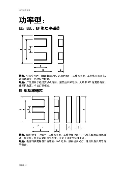
功率型:EE、EEL、EF型功率磁芯特点:引线空间大,绕制接线方便。
适用范围广、工作频率高、工作电压范围宽、输出功率大、热稳定性能好。
用途:广泛应用于程控交换机电源、液晶显示屏电源、大功率UPS逆变器电源、计算机电源、节能灯等领域。
EI型功率磁芯特点:结构紧凑、体积小、工作频率高、工作电压范围广、气隙在线圈顶端耦合紧、损耗低。
损耗与温度成负相关,可防止温度的持续上升。
用途:电源转换变压器及扼流圈、DVD电源、照相机闪光灯、通讯设备及其它电子设备。
PEE、PEI功率磁芯ER功率磁芯特点:耦合位置好,中柱为圆形,便于绕线且绕线面积增大,可设计功率大而漏感小的变压器。
用途:开关电源变压器,脉冲变压器,电子镇流器等。
ETD型功率磁芯特点:中柱为圆形,绕制接线方便且绕线面积增大,可设计出功率大且漏感小的变压器。
其他如组装成本,安规成本,电磁屏蔽,标准化难易等各方面都很出色。
用途:开关电源,传输变压器,电子镇流器。
广泛应用于家电、通讯、照明、医疗设备、办公自动化、军品、OA设备、电子仪器、航空航天等领域。
EQ/EQI型功率磁芯EP型功率磁芯特点:具有磁屏蔽效果好、分布电容小、传输衰耗低、电感量高、漏感小、磁场分布均匀等优点,且骨架配有多路接头,易设计多路输出变压器。
用途:宽带变压器、电感器、隔离变压器、匹配变压器,广泛应用于程控交换机终端和精密电子设备等领域。
EFD型功率磁芯特点:具有热阻小、衰耗小、功率大、工作频率宽凳使用优点。
成品重量轻、结构合理、易表面贴装。
用途:广泛应用于体积小而功率大的变压器,如精密仪器、模块电源、计算机终端输出等。
EPC功率磁芯特点:具有热阻小、衰耗小、功率大、工作频率宽、重量轻、结构合理、易表面贴装、屏蔽效果好等优点,但散热性能稍差。
用途:广泛应用于体积小而功率大且有屏蔽和电磁兼容要求的变压器,如精密仪器、程控交换机模块电源、导航设备等。
特点:体积小、感抗高、绕线方便、磁屏蔽及散热效果均衡。
磁芯参数对照表
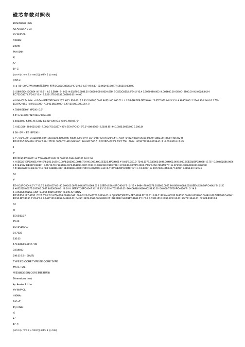
EFD103F310.5*5.2*2.70.00847.2011.60500.0023.70171.000.450.026
8H EFD123F312.5*6.2*3.50.018711.4016.38700.0028.50325.000.900.047.68H EFD153F315*7.5*4.650.047015.0031.35780.0034.00510.00 1.400.068.88H EFD203C8520*10*6.650.155031.0050.001300.0047.001460.00 3.500.2713.58H EFD253C9025*12.5*9.10.393858.0067.892200.0057.003300.008.000.3816.410H EFD303C9030*15*9.10.602869.0087.362100.0068.004700.0012.000.54