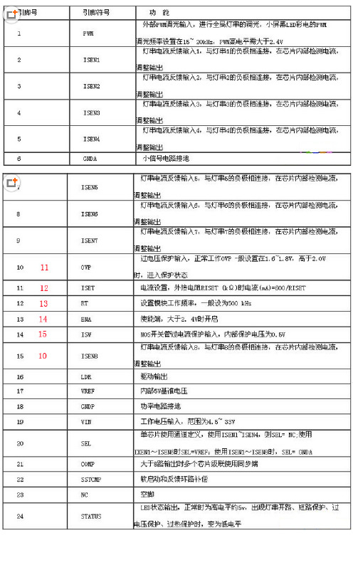
OZ 引脚功能及实测电压
OZ960引脚定义

OZ96010/23/01OZ960-DS-1.6 Page 1Intelligent CCFL Inverter ControllerFEATURES• Supports wide-range voltage input applications (8v to 20v)• Built-in intelligence to manage ignition and normal operation of CCFLs• Reduces the number of components and board size by 30% compared with conventional designs• 85% efficiency vs. typical 70% efficiency of conventional designs• Zero-voltage-switching full bridge topology • Built-in internal open-lamp and over-voltage protections• Integrated burst mode control, and wide dimming range (10% to 100%) with integrated burst mode control • Supports multiple CCFL lamps• Simple and reliable 2-winding transformer design• Constant-frequency design eliminates interference with LCDs •Low stand-by powerORDERING INFORMATIONOZ960S - 20-pin plastic SSOP 150mil OZ960I S - 20-pin plastic SSOP 150mil OZ960G - 20-pin plastic SOP 300mil OZ960I G - 20-pin plastic SOP 300mil OZ960D - 20-pin plastic DIP 300mil OZ960I D - 20-pin plastic DIP 300milGENERAL DESCRIPTIONThe OZ960 is a unique, high-efficiency, Cold Cathode Fluorescent Lamp (CCFL) backlight inverter controller that is designed for wide input voltage inverter applications. Additionally, the OZ960 performs the lamp dimming function with an analog voltage or low frequency Pulse Width Modulation (PWM) control.Operating Principle:Operating in a zero-voltage switching, full-bridge configuration, the inverter circuit achieves a very high efficiency power conversion. In addition, the transformer in the OZ960 does not require any specific gap-less arrangement. The simple, low cost transformer provides designers a high degree of design flexibility in specifying transformers. Setting the switching frequency higher than the resonant frequency of a high-quality-factor resonant tank circuit yields a good-quality waveform received, at the CCFL voltage and current.The OZ960 operates at a single, constant frequency in a phase-shift PWM mode. Intelligent open-lamp and over-voltage protections provide design flexibility so various transformer models/manufacturers may be used. The built-in burst mode control provides a wide dimming range and simplifies the application circuit designs. Both operating and burst-mode frequencies are user-programmable parameters.The single stage design results in a low cost, reliable transformer without expensive, less reliable secondary fold-back treatment. The transformer does not require a more expensive center tapped primary.The OZ960 is available in a 20-pin SSOP package. It is specified over the commercial temperature range of 0°C to +70°C, and the industrial temperature range of -40°C to +85°C.FUNCTIONAL BLOCK DIAGRAMRefer to the functional block diagram in Figure 2, page 3, and the Pin Description Table on page 4.A precision reference provides a reference voltage for both internal and external uses. An oscillator circuit generates a user-programmable operating frequency with an external capacitor and a timing resistor. In addition, another resistor to program striking frequency is provided. The drive circuit consists of four outputs. These are designed to achieve zero-voltage switching, full-bridge applications. An error amplifier is provided to regulate the CCFL current. The Soft-start circuit offers a gradual increase of the power to the CCFL during the ignition period. The over-voltage protection block offers a regulated striking voltage for CCFLs. The striking time is programmable simply through an external component. The open-lamp protection is integrated in the protection block. This block intelligently differentiates the striking condition and open-lamp condition. ENA circuitry enables the operation of the IC through a TTL signal interface. Wide-dimming control is achieved through the burst-mode control block.OZ960TYPICAL APPLICATION CIRCUITF 1V I N :8.0V ---22V E N A :0V --1.0V D i s a b l e ;2.0V ---3.3V E n a b l e D I M :3V M a x .B r i g h t n e s s ;1.2V M i n .B r i g h t n e s s S t r i k i n g f r e q u e n c y :74K H z -82K H z O p e r a t i n g f r e q u e n c y :56K H z -64K H zJ 1OZ960CTIMR OVP ENA SST VDDA GNDA REF RT1 FB CMP NDR_B PDR_A CT RT PGND LCT DIM LPWM PDR_C NDR_DACTIVE"HIGH"Figure 2. Functional Block DiagramPIN DESCRIPTIONNo. I/O DescriptionNames PinCTIMR 1 I Capacitor for CCFL ignition durationOVP 2 I Output voltage sense Vth=2.0VENA 3 I Enable input; TTL signal is applicablecapacitorSoft-startSST 4 IVDDA 5 I Voltage source for the ICGNDA 6 I Analog signal ground referenceREF 7 O Reference voltage output; 2.5V typicalRT1 8 I Resistor for programming ignition frequencyFB 9 I CCFL current feedback signalCMP 10 O Compensation output of the current error amplifierNDR_D 11 O NMOSFET drive outputPDR_C 12 O PMOSFET drive outputLPWM 13 O Low-frequency PWM signal for burst-mode dimming controlDIM 14 I Input analog signal for burst-mode dimming controlLCT 15 I Triangular wave for burst-mode dimming; frequencyPGND 16 I Power ground referenceRT 17 I Timing resistor set operating frequencyCT 18 I Timing capacitor set operating frequencyPDR_A 19 O PMOSFET drive outputNDR_B 20 O NMOSFET drive outputABSOLUTE MAXIMUM RATINGS WITHRESPECT TO INPUT POWER SOURCERETURN REFERENCEVDDA 7.0V(1)GNDA, PGND +/- 0.3VLogic inputs -0.3V to VDD +0.3VOZ960OZ960IOperating temp. 0o C to 70o C -40o C to 85o COperating junction temp. 150 o CStorage temp. -55 o C to 150 o CRECOMMENDED OPERATING RANGEVDDA 4.7V ~ 5.5VFosc 30 KHz to 150 KHzRosc 50 k to 150 kNote (1): The “Absolute Maximum Ratings” are those values beyond which the safety of the device cannot be guaranteed. The device should not be operated at these limits. The “Functional Specifications” table will define the conditions for actual device operation. Exposure to absolute maximum rated conditions for extended periods may affect device reliability.FUNCTIONAL SPECIFICATIONSParameter Symbol Test Conditions Limits UnitVDDA=5V; Tamb = 25o C Min Typ MaxReference VoltageNominal voltage Vref I load = 0.1mA 2.37 2.5 2.63 VLine regulation VDDA = 4.7V – 5.3V - 4 - mV/V Load regulation I load = 0.025 mA to 0.25 mA - 2 - mV/mA High Frequency OscillatorInitial accuracy fosc CT = 100pF, RT = 120k(1)5357 60 KHz Ramp peak - 3.0 - VRamp valley - 1.0 - V Temp. stability TA = 0 o C to 70o C - 200 - ppm/ o CLow Frequency OscillatorInitial accuracy See Table 1, page6Ramp peak 2.85 3.0 3.15 VRamp valley 0.94 1.0 1.06 VLow Frequency PWMDuty Cycle Range 0 - 100 %Error AmplifierInput offset voltage - 7 - mVInput voltage range 0 - VDD-1.5V VOffset current at FB pin - - 100 nAReference voltage at non-inverting input pin (internal) V ADJ 1.191.251.31VOpen loop voltage gain - 80 - dB Unity gain bandwidth - 1.0 - MHz Power supply rejection - 60 - dB ThresholdOver Voltage Protection 1.90 2 2.15 V SupplySupply current I OFF ENA=low -150200µASupply current I ONENA = high; VDDA = 5V;Vdim = 2V; LPWM = 50k(2)Ca=Cb=Cc=Cd=2nF(3)HF = 60kHz; LF = 185Hz- 4.4 5.5 mASST current See Table 1, page6 CTIMR current See Table 1, page6 NDR-PDR OutputOutput resistance Rp Current source - 27 - ΩOutput resistance Rn Current sink - 14 - ΩParameterSymbolTest ConditionsLimits Unit Max. / Min. OverlapVDDA = 5V; Tamb = 25o C Min Typ MaxMin. Overlap between diagonal switches HF = 60kHz Ca=Cb=Cc=Cd=2nF (3)3.04.55.5%Max. Overlap between diagonal switches HF = 60kHz Ca=Cb=Cc=Cd=2nF (3)78 81 84 % Brake before MakePDR_A / NDR_B See Table 1, below PDR_C / NDR_DSee Table 1, belowParameterSymbol Test ConditionsLimits Unit Limits UnitMin Typ Max Min Typ MaxLow Frequency OscillatorInitial accuracyfosc LCT = 6.8nF, LPWM = 50k (2)160 220 250 Hz150220340HzSupplySST current I SST 4.9 7.5 10 µA 4.9 6.0 12 µA CTIMR current I CTIMR2.23.34.5 µA2.03.0 5.2 µABrake before MakePDR_A / NDR_B HF = 60kHz 250 380 530 ns 250 380 565 ns PDR_C / NDR_DHF = 60kHz250 380 520 ns 250 380 545 ns ThresholdEnable1.35 1.50 1.65 V 1.25 1.50 1.65 VNote (1)CT: capacitor from CT (Pin 18) to ground RT: resistor from RT (Pin 17) to groundNote (2)LCT: capacitor from LCT (Pin 15) to ground LPWM: resistor from LPWM (Pin 13) to groundNote (3)Ca: capacitor from PDR_A (Pin 19) to VDDA Cb: capacitor from NDR_B (Pin 20) to ground Cc: capacitor from PDR_C (Pin 12) to VDDA Cd: capacitor from NDR_D (Pin 11) to groundTable 1. Low Frequency Oscillator, Supply and Brake before Make Specifications for OZ960 and OZ960IFUNCTIONAL INFORMATION1. Steady-State OperationRefer to the schematic shown in Figure 1, the OZ960 drives a full-bridge power train where the transformer couples the energy from the power source to the secondary CCFL load. The switches in the bridge denoted as QA, QB, QC and QD are configured such that QA and QB, QC and QD are turned on complementarily. The duration of QA and QD, QB and QC turn on simultaneously determines an amount of energy put into the transformer which in turn delivers to the CCFL. The current in CCFL is sensed via resistor R9 and regulated through the adjustmentof the turn-on time for both diagonal switches. This is accomplished through an error amplifier in the current feedback loop. A voltage loop is also established to monitor the output voltage so thata programmable striking voltage is achieved. The OVP represents the peak-detect signal of the voltage on the output of the transformer. A soft-start circuit ensures a gradual increase in the input and output power. The soft-start capacitor determines the rate of rise of the voltage on SST pin where the voltage level determines the on-time duration of QA and QD, QB and QC diagonal switches. This minimizes the surge impacts in circuit designs.Apply enable signal to the ENA pin of the IC after the bias voltage applied to VDDA initiates the operation of the circuit. The output drives, include PDR_A, NDR_B, PDR_C and NDR_D put out a complementary square pulse. The frequency is determined by R4 and C5 where they are connected to RT and CT pins respectively. Initially, the energy converted from the power source to the CCFL is low due to the soft start function. It increases as soft start capacitor voltage increases linearly with time. The voltageat the secondary side of the transformer T1 increases correspondingly. This process continues until the CCFL current is detected and reaches a regulated value. The output of the error amplifier, CMP, follows the feedback signal, commands a proper switching among the four output drives to maintain current regulation. The operations of the four switches are implemented with zero-voltage-switching to provide a high-efficiency power conversion.In the case of open-lamp condition, the OZ960 provides a programmable striking-frequency intelligence to optimize the ignition scheme. Thisis implemented through resistor R5. Effectively,R5 is in parallel with R4 to yield a required striking frequency. In addition, the striking time is also programmable through the capacitor C8. Striking voltage, or the open-lamp voltage, is regulated through a voltage feedback loop where output voltage is monitored. The signal, being sent to the OVP pin, commands the output drivesto provide the desired output voltage. This design provides high degree of flexibility while maintaining OZ960 a very high integration device.One protection feature needed is removing the lamp during normal operation. The OZ960 senses the missing current signal through current amplifier, it shuts off the output drives and stay in the latched mode. This is differentiated intelligently with turning on the inverter while CCFL is not connected. Recycle of the IC poweris necessary to resume normal operation. Dimming control: dimming control of the inverteris implemented by adjusting the amount of energy processed and delivered to the CCFL. A PWM burst-mode scheme is internally generated which provides 0% to 100% wide dimming control. An input analog voltage signal is fed into DIM pin and determines the dimming level of the CCFL. The burst-mode frequency is programmable through a capacitor C10 as shownin the schematic.The OZ960 inverter operates in a constant frequency mode. This eliminates any undesired interference between inverter and LCD panels where the interference is usually associated with variable-frequency designs.Symmetrical drive to the power transformer givesa very dynamic choice of selecting transformers. This vulnerable design offers flexibility to the system designers to choose transformer sources. There is no limitation to the gap-less transformer. 2. CCFL Ignition TimeIgnition time for CCFLs varies with CCFL length, diameter, module package and temperature. The OZ960 provides a flexible design where a capacitor is connected to CTIMR pin to determine the necessary striking time. An approximate of the timing calculation is:T[second] = C[uF]This capacitor remains reset at no charge if lampis connected and at normal operation.3. ProtectionOpen-lamp protection in the ignition period is provided through both OVP and CTIMR to ensurea rated voltage is achieved and a required timingis satisfied. Removal of the CCFL during normal operation will trigger the current amplifier output and shuts off the inverter. This is a latch function.4. OVPThe OVP threshold is set at 2V nominal. When the output voltage reaches the threshold, it commands the PWM controller to maintain the driving level. This ensures that output gets sufficient striking voltage while operating the power transformer safely.5. ENAApplying positive TTL logic to the ENA pin enables the operation of the IC. The threshold of the ENA is set at 1.5V. Apply logic low to the ENA pin will disable the operation of the inverter. Toggle this signal allows the on/off tests for the inverter.6. Soft-Start -- SSTThe soft-start function is provided with a capacitor connected to SST pin. The soft-start time is not related to the striking time for the CCFL. It simply provides a rate of rise for the pulse width where diagonal switches are turned on. Normally, a 0.47uF capacitor is connected. 7. Error AmplifierThe CCFL current is regulated through this error amplifier. It also provides an intelligence of differentiating open-lamp striking versus removing the lamp during normal operation. The non-inverting reference is at 1.25V nominal.8. Operating frequencyA resistor RT and a capacitor CT determine the operating frequency of OZ960. The frequency is calculated as:68.5•104f[kHz] =C T[pF]•R T[kΩ]The OZ960 also provides an optional striking frequency as desired. CCFL in a LCD module possesses parasitic that may require different striking voltage and frequency. This add-on feature could optimally accomplish the ignition process so that the CCFL life could be extended. When RT1 is used, it is connected in parallel with RT during the ignition period.9. Burst-Mode Dimming ControlThe OZ960 integrates a burst-mode dimming function to perform a wide dimming control for the CCFLs. The burst-mode frequency is determined by a capacitor C10 connected to LCT pin. The frequency can be calculated approximately by:1496f[Hz] =C LCT[nF]The Dim pin compares with the triangle wave in LCT and yields a proper pulse width to modulate the CCFL current. This pulse can also be monitored through LPWM pin. The peak and valley of the LCT signal is 3V and 1V respectively.10. Output DrivesThe four output drives are designed so that switches QA and QB, QC and QD never turn on simultaneously. These include two NMOS andtwo PMOS transistors. The configurationprevents any shoot-through issue associated with bridge-type power conversion applications. Adjusting the overlap conduction between QAand QD, QB and QC, the CCFL current regulation is achieved. This overlap is also adjusted while the voltage applied from the battery varies. At a specific CCFL current, the input power is maintained almost constant.PACKAGE INFORMATION (SSOP 150mil)PACKAGE INFORMATION (SOP 300mil)PACKAGE INFORMATION (DIP 300mil)Ee Bθ°DE 1IMPORTANT NOTICENo portion of O2Micro specifications/datasheets or any of its subparts may be reproduced in any form, or by any means, without prior written permission from O2Micro.O2Micro and its subsidiaries reserve the right to make changes to their datasheets and/or products or to discontinue any product or service without notice, and advise customers to obtain the latest version of relevant information to verify, before placing orders, that information being relied on is current and complete. All products are sold subject to the terms and conditions of sale supplied at the time of order acknowledgment, including those pertaining to warranty, patent infringement, and limitation of liability.O2Micro warrants performance of its products to the specifications applicable at the time of sale in accordance with O2Micro’s standard warranty. Testing and other quality control techniques are utilized to the extent O2Micro deems necessary to support this warranty. Specific testing of all parameters of each device is not necessarily performed, except those mandated by government requirements.Copyright © 2002, O2Micro International Limited。
001 一体机 DELL 戴尔 inspiron ONE 2205 CN27 输出至LED灯条高压板OZ9998 各引脚电压
ISEN8_1 ISEN7_1 ISEN6_1 ISEN5_1 ISEN4_1 ISEN3_1 ISEN2_1 ISEN1_1 VLED
12 11 10 9 8 7 6 5 4 3 2 1 12 11 10 9 8 7 6 5 4 3 2 1
XS751
D
R734 R717 R719 R720 R721 0.05 0.05 0.05 0.05 0.05
fop=50/RT---- 500KHZ; Io=600/Riset----20mA
实物板上是13脚
实物板上是15脚 此脚如果直接接地是去掉过流保护
4 3
标记 数量 拟 制 审 核 工 艺 标准化 批 准
分区 单号 签名 日期
标记 数量 分区 单号 签名 日期
OZ9998
第1 张
2 1
KONKA 共1 张
XS701
VIN VIN ON/OFF PWM GND GND PSON
7 PIN
1 2 3 4 5 6 7
+24V R712 10K ENA R718 100K C722 102 VIN R708 C720 10uF C721 10uF
R707 DRV 10 IS
1 3
0805_2A Q703 ME50N06
STATUS NC SSTCMP COMP SEL VIN GNDP VREF LDR ISEN5 ISW ENA
24STATUS 23 22 21 20 19 18 17 16 DRV 15 14
IS ISEN5_1 VDD C716 2.2u R715 100 SYN
1 2 3 4 5 6
PWM ISEN1 ISEN2 ISEN3 ISEN4 GNDA ISEN8 ISEN6 ISEN7 OVP ISET RT
OZ9910应用电路图及脚位功能

OZ9910(7)脚ADI端外部设置的电阻R528实际未安装,使得该脚电压低于,工作于脉冲调光模式,调光脉冲来自驱动板的BRIGHTNESS端。
驱动板的开关信号通过R526加到O Z9910(8)脚,在电压大于2V时芯片启动。
C505可以防止干扰信号对ENA端造成的影响。
OZ9910启动后。
激励信号从(16)、(3)、(15)、(4)脚输出,到末级功率管的栅极。
该电路末级功率管采用的型号是AOP605L,为8脚贴片封装形式,内含一个P沟道场效应管和一个N沟道场效应管。
其主要参数分别为30V、75A、和-30V、-6.6A、25W。
可采用FDS8958A进行直接代换。
高频变压器T501和T502的初级并联,这样每个变压器负责两个灯管,会显着降低故障率。
变压器次级的R501、R502、C527、C530、D507、D508等元件构成高压取样电路。
此取样电压加到OZ9910(9)脚,如果(9)脚电压超过,芯片会执行保护动作,停止驱动输出。
D504、D501、D506、D502等元件对灯管电流进行取样,取样电压分别加到Q502~Q505的栅极。
正常工作时,Q502和Q505处于微导通状态,这几只场效应管实际上起到类似于可调电阻的作用。
Q501栅极电压很低,处于截止状态。
不影响ISEN电流检测电路的工作。
芯片根据IS1和IS2反馈值大小来调整输出脉冲宽度,稳定灯管亮度。
如果任意一个灯管开路,OP取样电压立刻降为0V,对应控制管Q502~Q505其中之一必将截止,其漏极电压升高,最终引发Q501栅极电压升高,Q501导通,将OZ9910(11)脚电位拉低,OZ9910内部计数器开始计数,如果内此电压依然很低,则判断灯管脱落,执行保护动作。
(1)CCFL不能点亮首先按照常规检查供电电路,再目测功率管是否烧焦炸裂。
对于高频变压器可以用电阻法进行判断。
由于这种电路的两个变压器参数完全一致,两路驱动输出电路也完全一致,因此相互比对,采用在路电阻测量法可以迅速找到损坏元件。
oz890 数据手册 编程使用说明介绍
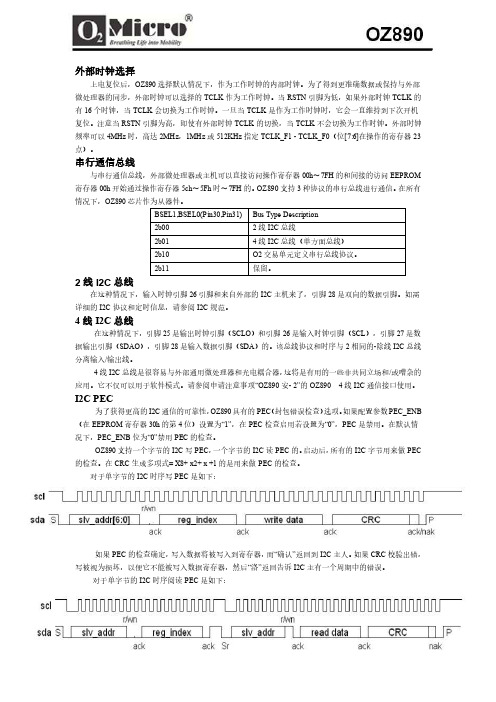
外部时钟选择上电复位后,OZ890选择默认情况下,作为工作时钟的内部时钟。
为了得到更准确数据或保持与外部微处理器的同步,外部时钟可以选择的TCLK作为工作时钟。
当RSTN引脚为低,如果外部时钟TCLK的有16个时钟,当TCLK会切换为工作时钟。
一旦当TCLK是作为工作时钟时,它会一直维持到下次开机复位。
注意当RSTN引脚为高,即使有外部时钟TCLK的切换,当TCLK不会切换为工作时钟。
外部时钟频率可以4MHz时,高达2MHz,1MHz或512KHz指定TCLK_F1 - TCLK_F0(位[7:6]在操作的寄存器23点)。
串行通信总线与串行通信总线,外部微处理器或主机可以直接访问操作寄存器00h〜7FH的和间接的访问EEPROM 寄存器00h开始通过操作寄存器5ch〜5Fh时〜7FH的。
OZ890支持3种协议的串行总线进行通信。
在所有情况下,OZ890芯片作为从器件。
2线I2C总线在这种情况下,输入时钟引脚26引脚和来自外部的I2C主机来了,引脚28是双向的数据引脚。
如需详细的I2C协议和定时信息,请参阅I2C规范。
4线I2C总线在这种情况下,引脚25是输出时钟引脚(SCLO)和引脚26是输入时钟引脚(SCL),引脚27是数据输出引脚(SDAO),引脚28是输入数据引脚(SDA)的。
该总线协议和时序与2相同的-除线I2C总线分离输入/输出线。
4线I2C总线是很容易与外部通用微处理器和光电耦合器,这将是有用的一些非共同立场和/或嘈杂的应用。
它不仅可以用于软件模式。
请参阅申请注意事项“OZ890安- 2”的OZ890 4线I2C通信接口使用。
I2C PEC为了获得更高的I2C通信的可靠性,OZ890具有的PEC(封包错误检查)选项。
如果配置参数PEC_ENB (在EEPROM寄存器30h的第4位)设置为“1”,在PEC检查启用若设置为“0”,PEC是禁用。
在默认情况下,PEC_ENB位为“0”禁用PEC的检查。
OZ964工作原理与维修
? 17/18脚RT/CT振荡电阻和电容。
常见OZ964引发故障:
? 不点灯,炸3.15A保险F100~F500中的一个
五个3.15A的保险是串联在20个双MOSFET组成的功率推挽电路及其激励电路上,其中F100串联在 Q114~Q117双MOSFET及0欧电阻R118、R119、R120、R121和其串联的激励三极管上,F200串联在Q214~Q217双MOSFET及0欧电阻R220、R221和其串联的激励三极管上,F300串联在Q314~Q317双MOSFET及0欧电阻R320、R321和其串联的激励三极管上,F400串联在Q414~Q417双MOSFET及0欧电阻R420、R421和其串联的激励三极管上,F500串联在Q514~Q517双MOSFET及0电阻R518、R519、R520、R521和其串联的激励三极管上。
四、维修实例
? 故障现象:不点灯,保险完好
故障检修:根据故障现象,基本判断故障范围在OZ964及其外围。首先测量ZO964的供电脚5脚,发现电压很低,几乎为0V,顺着5脚查看电路板,发现OZ964的供电是由三端稳压U4(78M05)提供,如图所示。测Q1发射极电压20V正常,集电极无电压输出,测Q8集电极电压0.2V,说明Q8已导通,背光控制电平已经送到Q8的基极,故障元件在Q1、R39、R38、R16,查得Q1开路,更换一只PNP电流大于100mA的三极管开机,发现U4(78M05)炸裂,说明其负载电流过大或本身损坏。断电测78M05输出脚对地电阻500欧左右,未见短路,更换一只新的78M05后开机,灯管点亮,故障排除。 ? 故障现象:不点灯,炸F100保险
转 OZ964工作原理与维修默认分类 2010-04-06 08:23:42 阅读231 评论0 字号:大中小 订阅
长虹液晶电视故障检修实例(下)
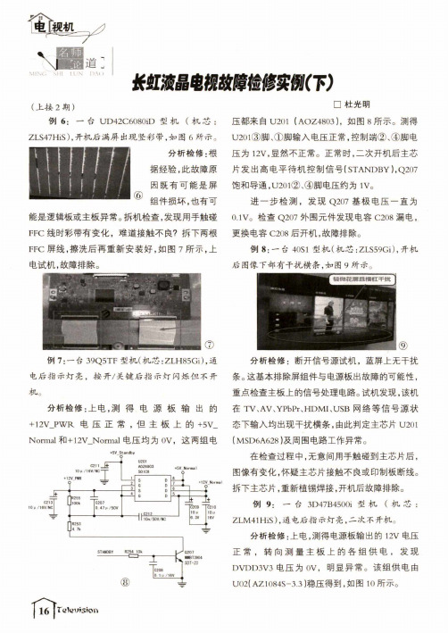
长虹液晶电视故障检修实倒(下〉(上接2期)例6: —台U D42C6080i D型机(机芯:ZLS47HiS),开机后满屏出现竖彩带,如图6所示。
分析检修:根据经验,此故障原因既有可能是屏组件损坏,也有可 能是逻辑板或主板异常。
拆机检查,发现用手触碰 FFC线时彩带有变化,难道接触不良?拆下两根 FFC屏线,擦洗后再重新安装好,如图7所示,上电试机,故障排除。
例7:—台39Q5T F型机(机芯:ZLH85Gi),通 电后指示灯亮,按开/关键后指示灯闪烁但不开 机。
分析检修:上电,测得电源板输出的+12V_P W R电压正常,但主板上的+5V_ Normal和+ 12V—Normal电压均为0V,这两组电□杜光明压都来自U201 (A OZ4803),如图8所示。
测得 U201③脚、①脚输入电压正常,控制端②、④脚电 压为12V,显然不正常。
正常时,二次开机后主芯 片发出高电平待机控制信号(STANDBY),Q207 饱和导通,U201②、④脚电压约为IV。
进一步检测,发现Q207基极电压一直为0.1V。
检查Q207外围元件发现电容C208漏电,更换电容C208后开机,故障排除。
例8:—台40S1型机(机芯:ZLS59Gi),开机 后图像下部有干扰横条,如图9所示。
⑨分析检修:断开信号源试机,蓝屏上无干扰 条。
这基本排除屏组件与电源板出故障的可能性, 重点检查主板上的信号处理电路。
试机发现,该机 在T V、A V、YPbPr、HDMI、U S B网络等信号源状态下输入均出现干扰横条,由此判定主芯片U201 (M SD6A628 )及周围电路工作异常。
S0T-23⑧在检查过程中,无意间用手触碰到主芯片后,图像有变化,怀疑主芯片接触不良或印制板断线。
拆下主芯片,重新植锡焊接,开机后故障排除。
例9: 一台3D47B4500i型机(机芯:ZLM41HiS),通电后指示灯亮,二次不开机。
分析检修:上电,测得电源板输出的12V电压 正常,转向测量主板上的各组供电,发现 D V D D3V3电压为0V,明显异常。
OZ964GN 芯片引脚功能
0.6
9
FB
电流反馈
1.27
10
CMP
电压控制系统补偿
2.12
11
NDR_D
N沟道场效应管门极驱动信号输出
2.42
12
PDR_C
P沟道场效应管门极驱动信号输出
2.49
13
LPWM
低频脉宽控制信号调光
1.17
14
DIM
低频脉宽控制信号调光占空直流电压输入
2.15
15
LCT
低频脉宽控制信号调光频率设定
1.22
16
DGND
功率场效应管驱动接地
0
17
RT
触发和工作频率时间设定电阻
建议不要测量该两脚电压(测量时,灯管闪烁,变压器发出异常叫声)
18
CT
触发和工作频率时间设定电容
19
PDR_A
P沟道场效应管门极驱动信号输出
2.51
20
NDR_B
N沟道场效应管门极驱动信号输出
2.43
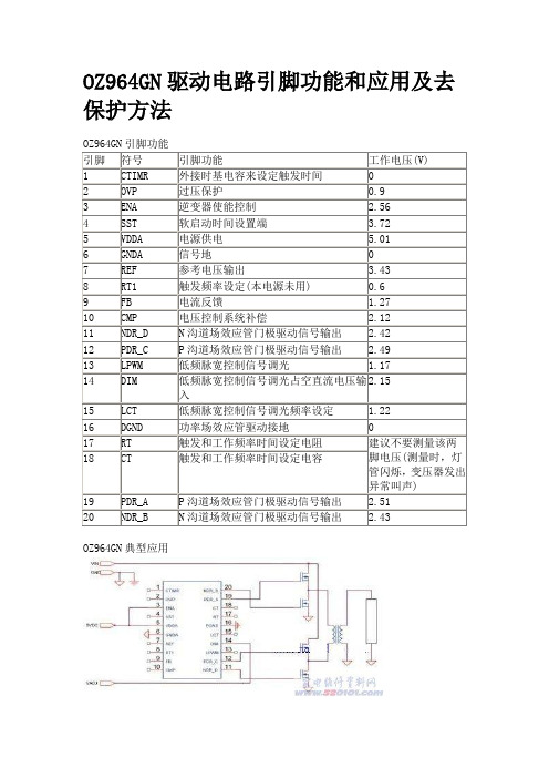
OZ964GN典型应用
OZ964GN去保护方法:OZ964GN②为保护取样电压反馈输入脚。OZ964GN①脚为点灯时间限制,当外接电容C13上充得的电压高于3v时,OZ964GN执行保护停止驱动输出。去保护时,只要将OZ964GN的①脚电压限制在保护动作电压就达到目的。于是在①脚的2.2UF电容上并联一个4148二极管即可。
OZ964GN驱动电路引脚功能和应用及去保护方法
OZ964GN引脚功能
引脚
符号
引脚功能
工作电压(V)
1
CTIMR
外接时基电容来设定触发时间
0
2
OVP
OZ960解析

下面就来计算如下图2所示电图V0到底多大才能使OVP脚到达2V。
V1=[C4/(C4+C6)]*V0
V1=VOVP+VD=2.0+0.7=2.7V
V0=[(C4+C6)/C4]*V1=[(12p+18n)/12p]*2.7=4100VP-P
也就是说只有输出电压的峰-峰值达到大于4100以上时,OVP电压才能到达2V。图2中R207/C204为峰值检测电路,其C204有对电压起到平滑的作用。
因为Q=I*t=V*C=>t=(V*C)/I
当C239电压被冲到3v,C239=1uF时,t=(3v*1uF)/3.0uA=1秒
2.第二PIN为OVP:此PIN为过电压保护PIN,输出电压被反馈到这一PIN上,当灯管被OPEN或是灯管坏掉时,OVP的电压就会升到2V,此时CTIMR电容被充电,当CTIMR被充到3V时,IC就会启动内部的保护功能,IC停止工作。
Stage2:Q2=>On;Q4=>On,当Q2自身二极管被打开时,在二极管的Source和Drain之间电压大约为VDS=-0.7V,这时Q2晶体管被打开,因此,Q2开关晶体管有零电压切换功能。此时电流方向:Q2TrC1Q4GND
- 1、下载文档前请自行甄别文档内容的完整性,平台不提供额外的编辑、内容补充、找答案等附加服务。
- 2、"仅部分预览"的文档,不可在线预览部分如存在完整性等问题,可反馈申请退款(可完整预览的文档不适用该条件!)。
- 3、如文档侵犯您的权益,请联系客服反馈,我们会尽快为您处理(人工客服工作时间:9:00-18:30)。
康佳LED42E310N/LED42MS92DC电源板OZ9902开机保护原理分析
以下是LED背光采用OZ9902的原理介绍和维修资料,供维修时参考:
修理前先目测,观察板有无烧器件,损坏器件、元器件虚漏焊等现象,检查相关元器件。
故障现象:开机指示灯正常,有声音,屏亮一下就灭。
故障分析:现象说明是背光部分故障,断开OZ9902的24脚保护,24脚输出高电压,关闭了电源部分的12V、100V输出,故问题在背光电路部分。
一、断开OZ9902的24脚开机,测量0Z9902的13-20脚电压,并与下图比较,判断是哪个脚故障。
OZ9902引脚功能及实测电压
脚位引脚功能实测电压1LED输入电压、欠压保护检测 5.1V 2ON9902工作电压输入12.0V 3芯片的ON/OFF端 5.2V 4基准点压输出 5.0V 5芯片工作频率设定和主辅模式设定 1.0V 6同步信号输入/输出,不用可以悬空0.0V 7第一通道的PWM调光信号输入 3.5V 8第二通道的PWM调光信号输入 3.5V 9模拟调光信号输入,不用可以设定为3V以上 2.6V 10保护延时设定端0.0V 11第一通道软启动和补偿设定 1.8V 12第二通道软启动和补偿设定 1.8V 13第二通道LED电流取样0.3V 14第二通道PWM调光驱动MOS端12.0V 15第二通道过压保护检测 2.1V 16第二通道OCP检测0.0V 17第一通道LED电流取样0.3V 18第一通道PWM调光驱动MOS端12.0V 19第一通道过压保护检测 2.1V 20第一通道OCP检测0.0V 21芯片接地0.0V 22第二通道升压MOS驱动 3.4V 23第一通道升压MOS驱动 3.5V 24异常情况下信号输出0.0V
1
OZ9902为双路驱动芯片,单路驱动简易图如下:
LED背光驱动电路
OZ9902引脚功能:
二、驱动电路升压过程:
驱动芯片OZ9902第2脚得到12V工作电压,第3脚得到高电平开启电平,第9脚得到调光高电平,第1脚欠压检测到4V以上的高电平时,OZ9902开始启动工作,从OZ9902的第23脚输出驱动脉冲,驱动V919工作在开关状态。
1、电路开始工作时,负载LED上的电压约等于输入VIN电压。
2、正半周时,V919导通,储能电感L909、L913上的电流逐渐增大,开始储能,在电感的两端形成左正右负的感应电动势。
3、负半周时,V919截止,电感两端的感应电动势变为左负右正,由于电感上的电流不能突变,与VIN叠加后通过续流二极管VD926给输出电容C900进行充电,二极管负极的电压上升到大于VIN电压。
4、正半周再次来临,V919再次导通,储能电感L909、L913重新储能,由于二极管不能反向导通,这时负载上的电压仍然高于VIN上的电压.正常工作以后,电路重复3、4步骤完成升压过程。
R919、R923、R929组成电流检测网络,检测到的信号送入芯片的20脚ISW11,在芯片内部进行比较,来控制V919的导通时间。
R909、R911、R914和R924是升压电路的过压检测电阻.连接至N905的第19脚的内部基准电压比较器.当升压的驱动电压升高时,其内部电路也会切断PWM信号的输出,使升压电路停止工作。
在N905内部还有一个延时保护电路,即由N905第10脚的内部电路和外接的电容C899组成.当各路保护电路送来起控信号时,保护电路不会立即动作,而是先给C899充电.当充电电压达到保护电路的设定阈值时,才输出保护信号.从而避免出现误保护现象,也就是说只有出现持续的保护信号时,保护电路才会动作。
三、PWM调光控制电路:
调光控制电路由V920等电路组成,V920受控于7脚的PWM调光控制,当第7脚为低电平时,第18脚的PROT1也为低电平,V920不工作.当第7脚为高电平时,第18脚的PROT11信号不一定为高电平,因为假如输出端有过压或短路情形发生,内部电路会将PROT1信号拉为低电平,使LED与升压电路断开。
R920、R926、R1025组成电流检测网络,检测到的信号送入芯片的第17脚ISEN1,第17脚为内部运算放大器+输入端,检测到的ISEN1信号在芯片内部进行比较,来控制V920的工作状态。
第11脚外接补偿网络,也是传导运算放大器的输出端.此端也受PWM信号控制,当PWM调光信号为高,放大器的输出端连接补偿网络.当PWM调光信号为低时,放大器的输出端与补偿网络被切断,因此补偿网络内的电容电压一直被维持,一直到PWM调光信号再次为高电平时,补偿网络才又连接放大器的输出端.这样可确保电路工作正常,以及获得非常良好的PWM调光反应。
在维修LED中如果发现屏亮一下保护,有声音,很多情况是国产LED灯珠或灯带质量不过关,一年左右就有损坏,引起整条LED灯带不工作,造成背光电路过压保护,如果判断已经过保修期,维修者可以打开屏更换LED灯珠或灯带,更换灯珠灯带过程在以后的资料中告诉大家。
OZ9902引脚功能分析
脚位符号功能
1UVLS欠压锁定检测(此脚电压小于3V,欠压动作,芯片无输出)
2VCC供电脚(电压输入范围8-16V)
3ENA使能脚(大于2V开始工作)
4VREF内部参考电压脚(此脚输出电压5V)
5RT工作频率设定脚(fop[khz]=6497/Rrt[k])
6SYNC同步脚,多个IC同时使用时有效。
如果只有一个IC,通过上拉电阻接到VREF。
7PWM1脉冲宽度调节1(FOR亮度条件),该芯片有两个通道,可分别独立调节,也可同时调节。
8PWM2脉冲宽度调节2(FOR亮度条件),该芯片有两个通道,可分别独立调节,也可同时调节。
9ADIM模拟调节(FOR亮度调节)。
10TIMER计时器(调整外接电容的大小,可以设置保护延迟的时间)
11SSTCM1通道1误差放大器输出(外接电阻、电容可设置软启动时间和相位补偿)。
12SSTCM2通道2误差放大器输出(外接电阻、电容可设置软启动时间和相位补偿)。
13ISEN2第二通道电流输入检测。
14PROT2第二通道PWM调光驱动输出。
15OVP2第二通道过压检测输入,电压大于3V时,进入保护状态,锁定无输出。
16ISW2第二通道升压MOS管电流检测。
取消过流保护此脚接地。
17ISEN1第一通道电流输入检测。
18PROT1第一通道PWM调光驱动输出。
19OVP1第一通道过压检测输入,电压大于3V时,进入保护状态,锁定无输出。
20ISW1第一通道升压MOS管电流检测。
取消过流保护此脚接地。
21GND芯片接地。
22DRV2第二通道驱动输出(为第二通道升压MOS提供驱动)
23DRV1第一通道驱动输出(为第一通道升压MOS提供驱动)
24FAULT故障输出脚(芯片工作时输出低电位,工作异常时外接QW904动作)
说明:15脚是第二通道过压检测输入;19脚第一通道过压检测输入。
取消过压保护把15脚和19脚接地。