
数字逻辑实验指导书(multisim)
实验一集成电路的逻辑功能测试一、实验目的1、掌握Multisim软件的使用方法。
2、掌握集成逻辑门的逻辑功能。
3、掌握集成与非门的测试方法。
二、实验原理TTL集成电路的输入端和输出端均为三极管结构,所以称作三极管、三极管逻辑电路(Transistor -Transistor Logic )简称TTL电路。
54 系列的TTL电路和74 系列的TTL电路具有完全相同的电路结构和电气性能参数。
所不同的是54 系列比74 系列的工作温度范围更宽,电源允许的范围也更大。
74 系列的工作环境温度规定为0—700C,电源电压工作范围为5V±5%V,而54 系列工作环境温度规定为-55—±1250C,电源电压工作范围为5V±10%V。
54H 与74H,54S 与74S 以及54LS 与74LS 系列的区别也仅在于工作环境温度与电源电压工作范围不同,就像54 系列和74 系列的区别那样。
在不同系列的TTL 器件中,只要器件型号的后几位数码一样,则它们的逻辑功能、外形尺寸、引脚排列就完全相同。
TTL 集成电路由于工作速度高、输出幅度较大、种类多、不易损坏而使用较广,特别对我们进行实验论证,选用TTL 电路比较合适。
因此,本实训教材大多采用74LS(或74)系列TTL 集成电路,它的电源电压工作范围为5V±5%V,逻辑高电平为“1”时≥2.4V,低电平为“0”时≤0.4V。
它们的逻辑表达式分别为:图1.1 分别是本次实验所用基本逻辑门电路的逻辑符号图。
图1.1 TTL 基本逻辑门电路与门的逻辑功能为“有0 则0,全1 则1”;或门的逻辑功能为“有1则1,全0 则0”;非门的逻辑功能为输出与输入相反;与非门的逻辑功能为“有0 则1,全1 则0”;或非门的逻辑功能为“有1 则0,全0 则1”;异或门的逻辑功能为“不同则1,相同则0”。
三、实验设备1、硬件:计算机2、软件:Multisim四、实验内容及实验步骤1、基本集成门逻辑电路测试 (1)测试与门逻辑功能74LS08是四个2输入端与门集成电路(见附录1),请按下图搭建电路,再检测与门的逻辑功能,结果填入下表中。
2.5 V(2)测试或门逻辑功能74LS32是四个2输入端或门集成电路(见附录1),请按下图搭建电路,再检测或门的逻辑功能,结果填入下表中。
2.5 V(3)测试非门逻辑功能74HC04是6个单输入非门集成电路(见附录1),请按下图搭建电路,再检测非门的逻辑功能,结果填入下表中。
VCC5V J5Key = SpaceX32.5 VVCC 0U3A 74HC04D_6V 78非门74HC04(4)测试与非门逻辑功能74LS00是四个2输入端与非门集成电路(见附录1),请按下图搭建电路,再检测与非门的逻辑功能,结果填入下表中。
2.5 V(5)测试或非门逻辑功能74LS02是四个2输入端或非门集成电路(见附录1),请按下图搭建电路,再检测或非门的逻辑功能,结果填入下表中。
2.5 V(6)测试异或门逻辑功能74LS86是四个2输入端异或门集成电路,请按下图搭建电路,再检测异或门的逻辑功能,结果填入下表中。
2.5 V(7)测试同或门逻辑功能74LS266是四个2输入端同或门集成电路,请按下图搭建电路,再检测同或门的逻辑功能,结果填入下表中。
2.5 V2、利用与非门组成其他逻辑门电路 ⑴组成与门电路将74LS00中任意两个与非门组成如下图所示的与门电路,输入端接逻辑电平开关,输出端接指示灯LED ,拨动逻辑开关,观察指示灯LED 的亮与灭,测试其逻辑功能,结果填入下表中。
2.5 V2.5 V⑵组成或门电路将74LS00中任选三个与非门组成如下图所示的或门电路,输入端接逻辑电平开关,输出端接指示灯LED ,拨动逻辑开关,观察指示灯LED 的亮与灭,测试其逻辑功能,结果填入下表中。
2.5 V⑶组成异或门电路将74LS00中的与非门按照下图所示的电路连线,输入端接逻辑电平开关,输出端接指示灯LED,拨动逻辑开关,观察指示灯LED的亮与灭,测试其逻辑功能,结果填入下表中。
2.5 V五、思考题请用或非门实现其他逻辑门电路,如与门、或门、非门、异或、同或。
实验二组合逻辑电路分析与设计一、实验目的1、掌握Multisim软件对组合逻辑电路分析与设计的方法。
2、掌握利用集成逻辑门构建组合逻辑电路的设计过程。
3、掌握组合逻辑电路的分析方法。
二、实验原理全加全减器是一个实现一位全加和全减功能的组合逻辑电路,通过模式变量M来控制全加/全减算术运算。
本实验可以使用74LS00,74LS86芯片来实现。
A i和B i分别表示二进制数A与B的第i位,C i表示A i-1和B i-1位全加时产生的进位,C i+1表示第A i和B i位全加时产生的进位,函数S和C i+1的卡诺图化简后为:S i=A i⊕B i⊕C iC i+1=B i C i+(C i+B i)(M⊕A i)=()⋅⊕⋅⋅⋅⋅BC M A B B C C三、实验设备1、硬件:计算机2、软件:Multisim四、实验内容及实验步骤1、根据实验原理构建全加全减器功能电路并测试逻辑功能。
Si Co2、利用逻辑分析仪测试第1步电路的功能及函数表达式。
U1A74LS86DU1B74LS86DU1C 74LS86DU2A74LS00DU2B74LS00D U3B74LS00DU4B74LS00D U5B74LS00DU6B74LS00DXLC2A B242123142019181716151222说明:上面的第一个图是测试C i+1,下面的图是测试S 的,要求分析出真值表及相应函数表达式及最简函数表达式。
3、利用设计全加全减器功能电路并测试逻辑功能。
B C D 424344454647 484950 515253 545556 574、利用逻辑分析仪测试第3步电路的功能。
(参考设计图略)五、思考题1、设X=AB,请用与非门实现Y=X3的组合逻辑电路。
2、设计一个血型配对指示器。
输血时供血者和受血者的血型配对情况如图所示,即(1)同一血型之间可以相互输血;(2)AB型受血者可以接受任何血型的输出;(3)O型输血者可以给任何血型的受血者输血。
要求当受血者血型与供血者血型符合要求时绿指示灯亮,否则红指示灯亮。
实验三血型关系检测电路的设计一、实验目的1.掌握组合逻辑电路的设计和测试方法。
2.学习选择和使用集成逻辑器件。
3.练习使用Multisim中的逻辑转换器。
二、实验类型设计型实验三、预习要求1. 复习组合逻辑电路的分析与设计方法。
2. 复习常用的组合逻辑器件的逻辑功能。
3. 画好实验电路的接线图,自拟实验步骤。
四、实验原理组合逻辑电路的设计是指根据给出的实际逻辑问题,求出实现这一逻辑关系的最简逻辑电路。
需要指出的是,这里所说的“最简”,在使用不同器件进行设计时有不同的含义。
对于小规模集成电路(SSI)为组件的设计,最简标准是使用的门最少,且门的输入端数最少;而对于以中规模集成电路(MSI)为组件的设计,则是以所用集成芯片个数最少、品种最少以及连线最少作为最简的标准。
设计步骤如下:1.根据设计任务,建立数字电路的模型,可以是真值表、卡诺图,也可以直接写出逻辑表达式。
2.跟据真值表或表达式填写卡诺图,进行化简。
化简的原则和最简函数的形式与使用的器件关系密切。
如欲使用与非门实现电路,应化简成与或式;如欲使用或非门实现电路则化简成或与式。
3.根据化简结果画出逻辑电路图。
4.根据逻辑电路图搭接电路。
5.测试并验证所设计的电路。
五、实验仪器装有Multisim 软件的计算机一台六、实验内容与要求人类的血型有4种:A、B、AB、O型。
在输血时,输血者和受血者的血型必须符合如图2.2.1所示的关系,即O型血可以输给任何血型的人,但O型血的人只能接受O型血;AB型血的人只能输给AB型血的人,但AB型血的人可以接受所有血型的人;A型血的人可以输血给A型和AB型血的人,而A型血的人能接受A型和O型血;B型血的人可以输血给B型和AB型血的人,而B型血的人能接受B型和O型血。
图2.2.1 输血关系图要求用与非门设计一个电路,用于判断输血者和受血者的血型是否符合输血条件,如果能够输血,则绿色指示灯亮(实验中用绿色探针代替):如果血型不合,则红色指示灯亮,并且发出警告声音(实验中用蜂鸣器代替)。
七、注意事项1. 输血者有4种情况,可用两位代码区分,同样受血者血型也可以用两位代码表示,这样整个电路的输入有四个变量,输出两个变量,分别表示能或不能。
2. 也可以用4个开关模拟A、B、AB、O 血型,(输血者和受血者共需要8个开关)对受血者和输血者的血型通过编码电路分别进行编码,之后根据要求设计血型检测电路。
八、实验报告1.说明设计过程,画出各逻辑电路图。
2.记录实验数据,总结实验心得。
九、思考题1.SSI为组件的设计方法与MSI为组件的设计方法有哪些区别,及其各自的优缺点。
2.不限定用于非门,还有哪些方法可以实现血型关系检测?实验四同步时序逻辑电路分析与设计一、实验目的1、掌握基本触发器的逻辑功能。
2、掌握集成触发器的功能和使用方法。
3、掌握同步时序逻辑电路的设计与分析的方法。
二、实验原理触发器是能够存储1位二进制码的逻辑电路,它有两个互补输出端,其输出状态不仅与输入有关,而且还与原先的输出状态有关。
触发器有两个稳定状态,用以表示逻辑状态“1”和“0”,在一定的外界信号作用下,可以从一个稳定状态翻转到另一个稳定状态,它是一个具有记忆功能的二进制信息存储器件,是构成各种时序电路的最基本逻辑单元。
1、JK触发器在输入信号为双端的情况下,JK触发器是功能完善、使用灵活和通用性较强的一种触发器。
本实验采用74LS112双JK触发器,是下降边沿触发的边沿触发器。
引脚逻辑图如图4-2所示:图4-2 JK触发器的引脚逻辑图JK触发器的状态方程为:+=+1nQ JQ KQ其中,J和K是数据输入端,是触发器状态更新的依据,若J、K有两个或两个以上输Q和Q为两个互补输出端。
通常把Q=0、Q=1的状态定为触入端时,组成“与”的关系。
Q=1,Q=0定为“1”状态。
JK触发器常被用作缓冲存储器,移位寄发器“0”状态;而把存器和计数器。
2、集成计数器计数器是数字系统中用的较多的基本逻辑器件,它的基本功能是统计时钟脉冲的个数,即实现计数操作,它也可用与分频、定时、产生节拍脉冲和脉冲序列等。
例如,计算机中的时序发生器、分频器、指令计数器等都要使用计数器。
计数器的种类很多。
按构成计数器中的各触发器是否使用一个时钟脉冲源来分,可分为同步计数器和异步计数器;按进位体制的不同,可分为二进制计数器、十进制计数器和任意进制计数器;按计数过程中数字增减趋势的不同,可分为加法计数器、减法计数器和可逆计数器;还有可预置数等等。
数字逻辑实验指导书(multisim)(精)

实验一集成电路的逻辑功能测试一、实验目的1、掌握Multisim软件的使用方法。
2、掌握集成逻辑门的逻辑功能。
3、掌握集成与非门的测试方法。
二、实验原理TTL集成电路的输入端和输出端均为三极管结构,所以称作三极管、三极管逻辑电路(Transistor -Transistor Logic 简称TTL电路。
54 系列的TTL电路和74 系列的TTL电路具有完全相同的电路结构和电气性能参数。
所不同的是54 系列比74 系列的工作温度范围更宽,电源允许的范围也更大。
74 系列的工作环境温度规定为0—700C,电源电压工作范围为5V±5%V,而54 系列工作环境温度规定为-55—±1250C,电源电压工作范围为5V±10%V。
54H 与74H,54S 与74S 以及54LS 与74LS 系列的区别也仅在于工作环境温度与电源电压工作范围不同,就像54 系列和74 系列的区别那样。
在不同系列的TTL 器件中,只要器件型号的后几位数码一样,则它们的逻辑功能、外形尺寸、引脚排列就完全相同。
TTL 集成电路由于工作速度高、输出幅度较大、种类多、不易损坏而使用较广,特别对我们进行实验论证,选用TTL 电路比较合适。
因此,本实训教材大多采用74LS(或74系列TTL 集成电路,它的电源电压工作范围为5V±5%V,逻辑高电平为“1”时≥2.4V,低电平为“0”时≤0.4V。
它们的逻辑表达式分别为:图1.1 分别是本次实验所用基本逻辑门电路的逻辑符号图。
图1.1 TTL 基本逻辑门电路与门的逻辑功能为“有0 则0,全1 则1”;或门的逻辑功能为“有1则1,全0 则0”;非门的逻辑功能为输出与输入相反;与非门的逻辑功能为“有0 则1,全1 则0”;或非门的逻辑功能为“有1 则0,全0 则1”;异或门的逻辑功能为“不同则1,相同则0”。
三、实验设备1、硬件:计算机2、软件:Multisim四、实验内容及实验步骤1、基本集成门逻辑电路测试 (1测试与门逻辑功能74LS08是四个2输入端与门集成电路(见附录1,请按下图搭建电路,再检测与门的逻辑功能,结果填入下表中。
multisim教程实验指导书第一章
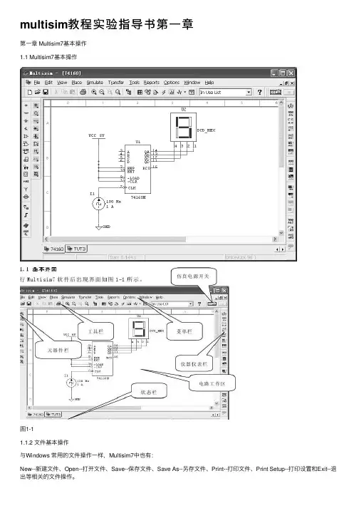
multisim教程实验指导书第⼀章第⼀章 Multisim7基本操作1.1 Multisim7基本操作图1-11.1.2 ⽂件基本操作与Windows 常⽤的⽂件操作⼀样,Multisim7中也有:New--新建⽂件、Open--打开⽂件、Save--保存⽂件、Save As--另存⽂件、Print--打印⽂件、Print Setup--打印设置和Exit--退出等相关的⽂件操作。
以上这些操作可以在菜单栏File ⼦菜单下选择命令,也可以应⽤快捷键或⼯具栏的图标进⾏快捷操作。
1.1.3 元器件基本操作常⽤的元器件编辑功能有:90 Clockwise--顺时针旋转90?、90 CounterCW--逆时针旋转90?、Flip Horizontal--⽔平翻转、Flip Vertical--垂直翻转、Component Properties--元件属性等。
这些操作可以在菜单栏Edit ⼦菜单下选择命令,或⽤Edit ⼦菜单右边显⽰的快捷键进⾏快捷操作,也可以选中元器件后右击⿏标选择相应命令。
例对三极管操作如图1-2所⽰:图1-21.1.4 ⽂本基本编辑对⽂字注释⽅式有两种:直接在电路⼯作区输⼊⽂字或者在⽂本描述框输⼊⽂字,两种操作⽅式有所不同。
1. 电路⼯作区输⼊⽂字单击Place / Text 命令或使⽤Ctrl+T 快捷操作,然后⽤⿏标单击需要输⼊⽂字的位置,输⼊需要的⽂字。
⽤⿏标指向⽂字块,单击⿏标右键,在弹出的菜单中选择Color 命令,选择需要的颜⾊。
双击⽂字块,可以随时修改输⼊的⽂字。
2. ⽂本描述框输⼊⽂字利⽤⽂本描述框输⼊⽂字不占⽤电路窗⼝,可以对电路的功能、实⽤说明等进⾏详细的说明,可以根据需要修改⽂字的⼤⼩和字体。
单击View/ Circuit Description Box 命令或使⽤快捷操作Ctrl+D ,打开电路⽂本描述框,如图1-3所⽰,在其中输⼊需要说明的⽂字,可以保存和打印输⼊的⽂本。
[工学]数字逻辑实验指导书
![[工学]数字逻辑实验指导书](https://360docs-1393072327.cos.ap-beijing.myqcloud.com/b319c6f85022aaea998f0fc8.webp)
《数字逻辑实验指导书》实验一组合逻辑电路分析与设计一、实验目的:1、掌握PLD实验箱的结构和使用;2、学习QuartusⅡ软件的基本操作;3、掌握数字电路逻辑功能测试方法;4、掌握实验的基本过程和实验报告的编写。
二、原理说明:组合电路的特点是任何时刻的输出信号仅取决于该时刻的输入信号,而与信号作用前电路的状态无关。
(一)组合电路的分析步骤:(二)组合逻辑电路的设计步骤首先根据给定的实际问题进行逻辑抽象,确定输入、输出变量,并进行状态赋值,再根据给定的因果关系,列出逻辑真值表。
然后用公式法或卡诺图法化简逻辑函数式,以得到最简表达式。
最后根据给定的器件画出逻辑图。
三、实验内容(一)组合逻辑电路分析:1.写出函数式,画出真值表;2.在QuartusⅡ环境下用原理图输入方式画出原理图,并完成波形仿真;3.将电路设计下载到实验箱并进行功能验证,说明其逻辑功能。
(必做)(二)1. 设计一个路灯的控制电路,要求在四个不同的路口都能独立地控制路灯的亮灭。
(用异或门实现)画出真值表,写出函数式,画出实验逻辑电路图。
在Quartus Ⅱ环境下实现设计,完成对波形的仿真,并将设计下载到实验箱并进行功能验证。
(必做)要求:用四个按键开关作为四个输入变量;用一个LED 彩灯(发光二极管)来显示输出的状态,“灯亮”表示输出为“高电平”,“灯灭”表示输出为“低电平”。
2. 设计一个保密锁电路,保密锁上有三个键钮A 、B 、C 。
要求当三个键钮同时按下时,或A 、B 两个同时按下时,或按下A 、B 中的任一键钮时,锁就能被打开;而当不符合上列组合状态时,将使电铃发出报警响声。
试设计此电路,列出真值表,写出函数式,画出最简的实验电路。
(用最少的与非门实现)。
在Quartus Ⅱ环境下实现设计,完成对波形的仿真,并将设计下载到实验箱并进行功能验证。
(选做)(注:取A 、B 、C 三个键钮状态为输入变量,开锁信号和报警信号为输出变量,分别用F 1用F 2表示。
数字逻辑实验指导书(multisim)

实验一集成电路的逻辑功能测试一、实验目的1、掌握Multisim软件的使用方法。
2、掌握集成逻辑门的逻辑功能。
3、掌握集成与非门的测试方法。
二、实验原理TTL集成电路的输入端和输出端均为三极管结构,所以称作三极管、三极管逻辑电路(Transistor -Transistor Logic )简称TTL电路。
54 系列的TTL电路和74 系列的TTL电路具有完全相同的电路结构和电气性能参数。
所不同的是54 系列比74 系列的工作温度范围更宽,电源允许的范围也更大。
74 系列的工作环境温度规定为0—700C,电源电压工作范围为5V±5%V,而54 系列工作环境温度规定为-55—±1250C,电源电压工作范围为5V±10%V。
54H 与74H,54S 与74S 以及54LS 与74LS 系列的区别也仅在于工作环境温度与电源电压工作范围不同,就像54 系列和74 系列的区别那样。
在不同系列的TTL 器件中,只要器件型号的后几位数码一样,则它们的逻辑功能、外形尺寸、引脚排列就完全相同。
TTL 集成电路由于工作速度高、输出幅度较大、种类多、不易损坏而使用较广,特别对我们进行实验论证,选用TTL 电路比较合适。
因此,本实训教材大多采用74LS(或74)系列TTL 集成电路,它的电源电压工作范围为5V±5%V,逻辑高电平为“1”时≥2.4V,低电平为“0”时≤0.4V。
它们的逻辑表达式分别为:图1.1 分别是本次实验所用基本逻辑门电路的逻辑符号图。
图1.1 TTL 基本逻辑门电路与门的逻辑功能为“有0 则0,全1 则1”;或门的逻辑功能为“有1则1,全0 则0”;非门的逻辑功能为输出与输入相反;与非门的逻辑功能为“有0 则1,全1 则0”;或非门的逻辑功能为“有1 则0,全0 则1”;异或门的逻辑功能为“不同则1,相同则0”。
三、实验设备1、硬件:计算机2、软件:Multisim四、实验内容及实验步骤1、基本集成门逻辑电路测试 (1)测试与门逻辑功能74LS08是四个2输入端与门集成电路(见附录1),请按下图搭建电路,再检测与门的逻辑功能,结果填入下表中。
数字逻辑设计实验室指导书说明书

LAB BROCHUREDigital Logic Design Lab DEPARTMENT OF ELECTRICAL ENGINEERINGCONTENTS...................................................................................................................... Lab Venue 3............................................................................................. Lab Objectives & Courses 3 Lab Description & Experiments 4....................................................................................................................................................................................... Hardware Experiments 5 ....................................................................................................... Verilog Experiments 6 Lab Resources 7...............................................................................................................DLD Lab Venue: Computer Interfacing Lab First Floor, Electrical DepartmentLab VenueThe Digital Logic Design Lab (DLD Lab) is one of the most important and well equipped lab of the Department of Electrical Engineering at University of Engineering and Technology, Lahore. This lab is conducted at the Computer Interfacing Lab situated at the first floor of the Electrical Engineering Department.Scope of the LabThe DLD Lab is for undergraduate coursework related to the course EE131. It is one of the core modules of B. Sc. Electrical Engineering therefore the lab has a significant importance in the department.Related CoursesThis lab is designed such that thestudents get a hands on familiaritywith the concepts they come acrossin the course EE131 that is the DigitalSystems course. This is anundergraduate course which dealswith the basics of digital systemsdesign and is a core module of theB. Sc. Electrical Engineeringcoursework as it provides theprerequisites for advance courses indigital electronics. Because of thesignificance of this course the DLDLab has been carefully designed tomeet the course requirement.Brief Overview of the LabThe Lab is well equipped withboth hardware and software facilitiesrequired by the students to performthe necessary experiments designedfor this lab. Details of the labequipment has been discussed in aproceeding section.Experiments are designed insuch a way that the students becomewell aware of the concepts they learnin the theory sessions. A list ofexperiments that are conducted inthis lab has also been mentioned in aproceeding section.Experiments are related to bothdigital hardware and VerilogProgramming.Objectives & CoursesLab Description & ExperimentsLab DescriptionThe Experiments in the Lab have been divided into two major portions:•Hardware Labs•Hardware Description Language (Verilog) LabsHardware Labs have been designed to familiarize students with the Combinational Digital Logic Design and Sequential Digital Logic Design through the implementation of Digital Logic Circuits using ICs of basic logic gates and some simple digital logic circuits.HDL (Verilog) Labs havebeen designed tofamiliarize students with theHDL based Digital DesignFlow. These labs introducestudents with differentlevels of coding available inVerilog i.e. Gate level,Dataflow level andBehavioral level. Xilinx ISE7.1 tools have been used inthese labs. Finally, theskills learnt in the HDLlabs are employed toimplement some digitallogic circuits on Spartan-3FPGA, using Xilinx StarterKit Development Board.Expected OutcomesWith the help of the twothreads of the labmentioned above, studentswill have clearunderstanding of all thethree paradigms ofimplementation of digitallogic circuits:•Implementation usingICs for basic logic gatesand simple circuits•Implementationthrough the Developmentof Dedicated IC(ASIC)•Implementationthrough ReconfigurableLogic (i.e. FPGA)This makes studentsadept in basic conceptsinvolved in digital logicdesign. The lab contributesa lot to the basic learning ofdigital systems.This shows theindispensability of theDLD Lab.List of ExperimentsList of experiments isgiven on page 5 and 6. Asmentioned before the labhas two major portionstherefore there are two listsof experiments one relatedto the hardware labs andthe other related to thehardware descriptionlanguage (verilog) labs. Allthese experiments aremandatory and each lab isfollowed by speciallydesigned assignments.A Lab DemonstrationA Digital Chip (inside view)TITLE TOPICS1To Verify the Behavior of Logic Gates using Truth Table and Familiarization with Digital Integrated Circuits Basic Logic Gates, Truth Table, Integrated Circuits2Implementation of Boolean Function using Logic Gates and Introduction to Hierarchical Design of Digital Logic Circuits Boolean Functions,Boolean Algebra,Hierarchical Design of Digital Logic Circuits3Familiarization with the Different Portions of the Datasheet fora Digital IC and Using the Datasheet to Gather RelevantInformation to Utilize the IC as a Component in another DigitalLogic Circuit Datasheet of a Digital Logic IC, Hierarchical Design of Digital Logic Circuits4Implementation of 8 bit Binary Comparator using 4 bit Binary Comparators Binary Comparator,Hierarchical Design of Digital Logic Circuits5Implementation of 4bit into 3bit Binary Multiplier using 4bit Binary Adders Binary Multiplication,Hierarchical Design of Digital Logic Circuits6Implementation of BCD Adder using 4bit Binary Adders, 4 to 7 Segment Decoder and 2Digit 7 Segment Display BCD addition,Hierarchical Design of Digital Logic Circuits7Implementing a Full Adder using(a) Decoder(b) Multiplexer Implementation of Boolean function using Decoder,Implementation of Boolean function using Multiplexer8Flip Flops Different Types of Flip Flops9To study the fundamentals of basic counters and to construct various types of counters CountersHardware ExperimentsTITLE TOPICS1Introduction to HDL based Digital Design Methodology HDL based Digital Design Flow usingVerilog,Introduction to Outsourcing Business Model2Introduction to Basic Syntax of Verilog and Gate level Modelingthrough implementation of half adder at gate level and itssimulation using Xilinx ISE tools Basic Concepts of Verilog, Modules and Ports, Gatelevel coding in Verilog,3Introduction to the concepts of Instantiation and HierarchicalDesign in Verilog through the implementation of full adderusing the previously designed half adder modulesHierarchical Design in Verilog4Introduction to the Concept of Vectors and Introduction to Dataflow modeling through implementation of half adder andfull adder at dataflow level Vectors in Verilog,Dataflow level coding in Verilog5Consolidation of the concepts of Dataflow level modeling and Introduction to the concept of Synthesis by the CAD tool Dataflow level coding in Verilog, Logic Synthesis6Introduction to Behavioral modeling through implementation ofhalf adder and full adder at behavioral level.Behavioral level coding in Verilog7Introduction to if else statement and case statement inBehavioral modeling through implementation of Multiplexerif else and case statements in Verilog8Introduction to the Concepts of Sequential Circuit anda TestBench module (Stimulus Block)Sequential circuits in Verilog, Concept of Testbench module in Verilog9Behavioral Level Coding of Basic Sequential Circuits andConsolidation of the concepts of TestBench module (StimulusBlock)Sequential circuits in Verilog10Introduction to Field Programmable Gate Array(FPGA) and Steps involved in its Programming Need for Reconfigurable Logic, Xilinx ISE Tools for Programming the Xilinx FPGAsVerilog ExperimentsLab ResourcesHardware ResourcesThe lab is fully equipped with all the hardware required to conduct the above mentioned experiments. The hardware resources of the lab are:•Pentium-IV PCs (with MS WinXp OS)•Hardware trainers for logic circuit design and analysis•Electronic Chips of all digital gates•Spartan-III FPGA board kits•Power SuppliesThese resources allowthe students to have ahands on experience ofbasic digital logic designconcepts. This activitygreatly leverages what thestudents learn in the theorysessions.Software ResourcesThe lab also consists ofthe software resourcesrequired by the studentsnamely:•Veriwell•ModelSim•Xilinx IDE•MatlabSoftware resources areequally important ashardware resources are.These software resourcesare sufficient for thestudents to performexperiments. Thesesoftwares provide thestudents with thenecessary platform to workon HDL that is the Verilog.These softwares are alsorequired to work with thesophisticated hardwareslike Spartan-III FPGAboards.The lab has all theresources whether relatedto hardware or software sothat the students becomeadept in the basic field ofdigital electronics.Students areencouraged to use the labresources to performactivities andexperiments which helpthem strengthen theirconcepts.Lab StaffLike other labs of thedepartment there is atrained and able staffconsisting of skilled labtechnicians that take careof the lab equipment.They also guidestudents about handlingthe lab equipment and theprecautionary measuresrequired for the studentswhile working in the lab.A Digital Circuit BoardA SimulationDIGITAL LOGIC DESIGN LAB1st Floor, Department of Electrical Engineering UNIVERSITY OF ENGINEERING & TECHNOLOGY, LAHORE-54890, PAKISTAN..pkurl:Ph: + 92 42 9029229, Fax: + 92 42 9250224Computer Interfacing Lab。
实验指导书(电路分析multisim)

对于上述零状态响应、零输入响应和全响应的过程,uC (t)和iC (t)的波形只有用长余辉 示波器才能直接显示出来,普通示波器难于观察。
如用方波信号源激励,RC 电路的方波响应,在电路的时间常数远小于方波周期时,前
5
半周期激励作用时的响应就是零状态响应,得到电容充电曲线;而后半周期激励为 0,相当
容量大小就代表时间常数的大小。如图 3 所示给出了电容容量较小时, C = 100μF 时,电
容的充放电波形,该波形近似为矩形波,充放电加快,上升沿和下降沿变陡。
4.2 二阶电路的过渡过程 1 创建电路:从元器件库中选择电压源、电阻、电容、电感、单刀双掷开关和虚拟示波器, 创建二阶电路如图 4 所示。
R1
1kHz
10Ω
0°
图 1 串联谐振电路 2、电路的幅频特性:单击运行(RUN)按钮,双击频率特性仪XBP1 图标,在Mode选项组 中单击Magnitude(幅频特性)按钮,可得到该电路的幅频特性,如图 2 所示。从图中所知, 电路在谐振频率f0处有个增益极大值,而在其他频段增益大大下降。需要说明的是,电路的 谐振频率只与电路的结构和元件参数有关,与外加电源的频率无关。本处电路所选的电源频 率为 1kHz,若选择其他频率,幅频特性不变。
7
切换开关,就能得到电容的充放电波形
图 3 电容容量较小时的充放电波形
说明: 1 当开关停留在触点 1 时,电源一直给电容充电,电容充到最大值 12V,如图 2 中电容充放 电波形的开始阶段。 2 仿真时,电路的参数大小选择要合理,电路的过渡过程快慢与时间常数大小有关,时间常 数越大,则过渡过程越慢;时间常数越小,则过渡过程越快。电路中其他参数不变时,电容
R
R
(自由分量)
Multisim数字逻辑转换实验
实验1 Multisim数字逻辑转换实验一、实验目的1、通过实验学习使用逻辑转换仪化简逻辑函数的方法。
2、通过实验学习使用逻辑转换仪分析逻辑图的方法。
二、实验设备计算机1台三、实验原理Multisim是美国国家仪器(NI)有限公司推出的以Windows为基础的仿真工具,适用于板级的模拟/数字电路板的设计工作。
它包含了电路原理图的图形输入、电路硬件描述语言输入方式,具有丰富的仿真分析能力。
非常适合数字电路的仿真分析,并且提供了功能丰富的虚拟仪器和元件。
其提供的虚拟数字逻辑转换仪可对8个逻辑变量的任意逻辑关系进行分析、化简、转换,非常适合简单数字电路的分析与设计,逻辑转换仪见图1-1所示。
数字逻辑转换仪可通过表达式输入框接受文本输入的逻辑关系表达式,式中逻辑变量名称限定为A、B、C、D、E、F、G、H共8个,其中A为最高位,H为最低位。
逻辑转换仪的输出为Out,逻辑关系中逻辑非用“’”来表示。
逻辑转换仪提供6种转换功能,见图1右侧,从上到下依次是:逻辑图转换成真值表功能;真值表转换成逻辑表达式功能;真值表转换成最简逻辑表达式功能;逻辑表达式转换成真值表功能;逻辑表达式转换成逻辑图功能;逻辑表达式转换成仅由与非门构成的逻辑图功能。
本实验将使用这些功能实现基本逻辑电路的分析与设计。
图1-1 逻辑转换仪四、实验内容1、逻辑函数的化简在表达式输入框中输入需化简的逻辑函数,并点击逻辑表达式转换成真值表功能按钮,并将转化结果记录在表1-1中。
逻辑函数如下:R=AB’CD’+A’E+BE’+CD’E表1-1 逻辑函数转换成成指标结果使用真值表转换成化简后逻辑表达式功能,并记录化简结果。
化简后R=A’E+AB’CD’+BE使用表达式转换成逻辑图功能,生成化简后R的逻辑图,并记录.使用表达式转换为仅由与非门构成的逻辑图功能,生成化简后R的逻辑图,并记录。
2、逻辑图的分析图1-2 逻辑图分析连接图1、实验逻辑图如图1-2,在Multisim数字器件库中,找到74LS138D和74LS10D,按图连接。
数字电路实验Multisim仿真完整版
数字电路实验M u l t i s i m仿真HEN system office room 【HEN16H-HENS2AHENS8Q8-HENH1688】实验一逻辑门电路一、与非门逻辑功能的测试74LS20(双四输入与非门)仿真结果二、门)三、与或非门逻辑功能的测试四、现路;一、分析半加器的逻辑功能二.74LS138接成四线-十六线译码器 00000001011110001111(2)用一片74LS153接成两位四选一数据选择器; (3)用一片74LS153一片74LS00和接成一位全加器(1)设计一个有A 、B 、C 三位代码输入的密码锁(假设密码是011),当输入密码正确时,锁被打开(Y 1=1),如果密码不符,电路发出报警信号(Y 2=1)。
以上四个小设计任做一个,多做不限。
还可以用门电路搭建实验三 触发器及触发器之间的转换1. D 触发器逻辑功能的测试(上升沿)2. JK 触发器功能测试(下降沿)Q=0Q=0略3. 思考题:(1)(2)(3)略实验四寄存器与计数器1.右移寄存器(74ls74 为上升沿有效)位异步二进制加法,减法计数器(74LS112 下降沿有效)也可以不加数码显示管3.设计性试验(1)74LS160设计7进制计数器(74LS160 是上升沿有效,且异步清零,同步置数)若采用异步清零:若采用同步置数:(2)74LS160设计7进制计数器略(3)24进制83进制注意:用74LS160与74LS197、74LS191是完全不一样的实验五 555定时器及其应用1.施密特触发器输入电压从零开始增加:输入电压从5V开始减小:2.单稳态触发器3.多谢振荡。
《数字逻辑》实验指导书
目录实验1: 基本逻辑门电路 (2)EDA设计实验的基本步骤和注意事项 (4)实验2: 译码器及其应用 (10)实验3 触发器、移位寄存器的设计和应用 (15)实验4: 计数器 (18)实验5: 数字系统的设计 (19)实验报告格式和内容 (20)实验1: 基本逻辑门电路一、实验目的1: 掌握各种门电路的逻辑功能及测试方法。
2: 学习用与非门组成其它逻辑门电路。
二、实验用的仪器、仪表TEC —5实验箱 74LS00二输入四与非门 三态门74LS125三、实验原理与非门的逻辑功能是: 当输入端中有一个或一个以上低电平时, 输出端为高电平。
只有当输入端全为高电平时, 输出端才为低电平(即有“0”得“1”, 全“1”出“0”)。
三态输出门是一种特殊的门电路。
它与普通的逻辑门电路不同, 它的输出状态除了高、低电平两种状态(均为低阻状态)外, 还有第三种状态,即高阻态。
处于高阻态时, 电路与负载之间相当于开路。
三态门主要用途之一是实现总线传输。
三态输出门符号与功能表如下(此例以低有效的使能器件为例)。
四、实验内容 1: 测试二输入与非门的逻辑功能与非门的输入端接逻辑开关电平, 输出端接发光二极管。
按表1-2所示测试与非门, 并将测试结果填入表中。
B A F •= 表1-1AB2: 学习用二输入与非门构成其他逻辑电路的方法, 并测试。
与门逻辑功能实现:根据布尔代数的理论, ,所以用2个与非门即可实现与门逻辑功能。
输入A 、B 接逻辑开关, 输出端接发光二极管。
参考表1-1, 设计表格, 并将测试结果填入表中。
或门逻辑功能实现:根据布尔代数的理论, ,所以用3个与非门即可实现或门逻辑功能。
输入A 、B 接逻辑开关, 输出端接发光二极管。
参考表1-1, 设计表格, 并将测试结果填入表中。
异或门逻辑功能实现:根据布尔代数的理论, ,根跟据此异或逻辑表达式经过变换, 逻辑图如下, 请自行验证此逻辑图的正确性, 同时思考如果直接据逻辑表达式画逻辑图, 效果如何, 近而体会变换的作用。
使用multisim进行数字逻辑电路建模与仿真说明书
DIGITAL LOGIC CIRCUIT MODELING AND SIMULATION WITH MULTISIMMultisim is a schematic capture and simulation program for analog, digital and mixed analog/digital circuits, and is one component of the National Instruments “Circuit Design Suite”.The basic steps in modeling and analysis of a digital logic circuit are:1.Open Multisim and create a “design”.2.Draw a schematic diagram of the circuit (components and interconnections).3.Design digital test patterns to be applied to the circuit inputs to stimulate the circuit and connect signal sourcesto the circuit inputs to produce these patterns.4.Connect the circuit outputs to one or more indicators to display the response of the circuit to the test patterns.5.Run the simulation and examine the results, copying and pasting Multisim windows into lab reports and otherdocuments as needed.6.Save the design.Step 1. Open Multisim and create a designThis creates a blank design called “Design1”, as illustrated in Figure 1. Save the file with the desired design name via menu bar File>Save As to use the standard Windows Save dialog.A previously saved design can be opened via File>Open. In the dialog window, navigate to the directory in which the design is stored, select the file, and click the Open button.Figure 1. Blank design with default name “Design 1.”Step 2. Draw a schematic diagram of the circuitPlace ComponentsA schematic diagram comprises one or more circuit components, interconnected by wires. Optionally, signal “sources” may be connected to the circuit inputs, and “indicators” to the circuit outputs. Each component is selected from the Multisim library and placed on the drawing sheet in the Circuit Window (also called the Workspace). The Multisim library is organized into “groups” of related components (Transistors, Diodes, Misc Digital, TTL, etc.). Each group comprises one or more “families”, within which the components are implemented with a common technology. For designing and simulating digital logic circuits in this course, “Misc Digital” (TIL family only) is used.The “Misc Digital” group has three families of components, of which family “TIL” contains models of generic logic gates, flip-flops, and modular functions. These components are technology-independent, which means that they have only nominal circuit delays and power dissipation, unrelated to any particular technology. Generic components can be used to test the basic functionality of a design, whereas realistic timing information requires the use of technology-specific part models, such as those in the TTL group.To place a component on the drawing sheet, select it via the Component Browser, which is opened via the component toolbar or the menu bar. From the menu bar, select Place>Component to open the Component Browser window, illustrated in Figure 2. You can also open this window by clicking on the Misc Digital icon in the component toolbar. On the left side of the window, select “Master Database”, group “Misc Digital”, and family “TIL”. The component panel in the center lists all components in the selected family. Scroll down to and click on the desired gate (NAND2 Figure 3); its symbol and description are displayed on the right side of the window. Then click the OK button. The selected gate will be shown on the drawing sheet next to the cursor; move the cursor to position the gate at the desired location, and then click to fix the position of the component. The component can later be moved to a different location, deleted, rotated, etc. by right clicking on the component and selecting the desired action. You may also select these operations via the menu bar Edit menu.Figure 2. Component Browser: Misc Digital TIL family NAND2 gate component selected.Figure 3. A third NAND2 gate is about to be placed on the drawing sheet.Figure 4 shows the schematic diagram with four placed components. Note that each placed gate has a “designator” (U2, U3, U4, U5), which can be used when referring to that gate. You can change a designator by right clicking on the component, selecting Properties, and entering the desired name on the Label tab.Figure 4. Schematic diagram with all placed components.Drawing WiresWires are drawn between component pins to interconnect them. Moving the cursor over a component pin changes the pointer to a crosshair, at which time you may click to initiate a wire from that pin. This causes a wire to appear, connected to the pin and the cursor. Move the cursor to the corresponding pin of the second component (the wire follows the cursor) and click to terminate the wire on that pin. If you do not like the path selected for the wire, you may click at a point on the drawing sheet to fix the wire to that point and then you can move the cursor to continue the wire from that point. You may also initiate or terminate a wire by clicking in the middle of a wire segment, creating a “junction” at that point. This is necessary when a wire is to be fanned out to more than one component input. A partially-wired circuit, including one junction point, is illustrated in Figure 5.Figure 5. Partially wired circuit, with one junction point.Step 3. Generating test input patterns.To drive circuit simulations, Multisim provides several types of “sources” and “instruments” to generate and apply patterns of logic values to digital circuit inputs. Sources are placed on the schematic sheet and connected to circuit inputs in the same way as circuit components, selecting them from the “Digital_Sources” family of the “Sources” group in the component browser. Note that there is a Place Source shortcut icon in the tool bar.There are three basic digital sources:1.DIGITAL_CONSTANT – this is a box with a constant logic 1 or 0 output, and would be used where the logic valueis not to be changed during simulation. To change the output value, right click on the box, select Properties, select the desired value on the Value tab, and click the OK button.2.INTERACTIVE_DIGITAL_CONSTANT – this is a clickable box that can be connected to a circuit input. Clicking onthe box toggles its output between 0 and 1. This can be used to interactively change a circuit input duringsimulation.3.DIGITAL_CLOCK – this is a box that produces a repeating pulse train (square waveform), oscillating between 0and 1 at a specified frequency. To set the frequency and duty cycle, right click on the box, select Properties,select the desired frequency and duty cycle value on the Value tab, and click the OK button.Figure 6 shows the circuit of Figure 5 with an INTERACTIVE_DIGITAL_CONSTANT connected to each input. Note that the initial state of each is logic 0. Since this circuit has only three inputs, all 8 input patterns can be produced (to generate a truth table for the circuit) by manually toggling the inputs.Figure 6. INTERACTIVE_DIGITAL_CONSTANT sources connected to circuit inputs.Step 4. Connect circuit outputs to indicatorsTo facilitate studying the digital circuit output(s), Multisim provides a variety of “indicators”. For digital simulation, the most useful are digital “probes”, hex displays, and the Logic Analyzer instrument. A probe, illustrated in Figure 7, displays a single digital value as ON or OFF (the probe is “illuminated” indicating an ON condition). The PROBE family of the Indicators group includes a generic PROBE_DIG and several PROBE_DIG_color indicators (color = BLUE, GREEN, ORANGE, RED, YELLOW). The probe in Figure 7 is PROBE_DIG_BLUE. This circuit can be verified by manually changing the three INTERACTIVE_DIGITAL_CONSTANT inputs to each of the 8 possible combinations, and recording the probe value for each combination to create a truth table.Figure 7. DIGITAL_PROBE_BLUE connected to circuit output.Step 5. Run the simulationA simulation is initiated by pressing the Run (green arrow) button in the toolbar or via the menu bar via Simulate>Run. You may simulate the circuit by clicking on the keys to change the input values and observe the output changes through the LED indicator.You may capture any window and paste it into a Word or other document for generating reports. An individual window is captured by pressing the ALT and Print Screen keys concurrently. You may then “paste” the captured window into a document via the editing features of that document. To capture a circuit diagram in the main window, the simplest method is via the menu bar Tools>Capture Screen Area. This produces a rectangle whose corners can be stretched to include the screen area to be captured; the “copy” icon on the top left corner is pressed to copy the area, which may then be pasted into a document.Step 6. Save the design and close MultisimThe simplest way to save a design is to click the Save icon in the Design Toolbar on the left side of the window, directly above the design name. Alternatively, you may use the standard menu bar File>Save.Multisim is exited as any other Windows program.-This document is a modified and short version of /department/ee/elec2210/.Appendix: Creating subcircuits and hierarchical blocks (from NI Multisim manual)Complete the following steps to place a new subcircuit:1. Select Place»New subcircuit. The Subcircuit Name dialog box appears.2. Enter the name you wish to use for the subcircuit, for example, “PowerSupply” andclick OK. Your cursor changes to a “ghost” image of the subcircuit indicating that thesubcircuit is ready to be placed.3. Click in the desired location to place the subcircuit.4. Double-click on the new subcircuit and select Open subsheet from the Label tab ofthe Hierarchical Block/Subcircuit dialog box that displays. An empty design sheetappears.5. Place and wire components as desired in the new subcircuit.6. Select Place»Connectors»Hierarchical connector, and place and wire the connector asdesired. Repeat for all required hierarchical connectors.When you attach a hierarchical connector to a wire, the net name for the wire that you connect it to does not change if it has a Preferred net name (user-assigned via the NetProperties dialog box). If the net name on the wire is auto-named, it changes to match theconnector.7. Select the sheet that contains the subcircuit from the Hierarchy tab of the DesignToolbox.OrSelect View»Parent sheet.This command moves you up to the next sheet in the hierarchy. If you have multiple nested circuits and are viewing, for example, a subcircuit within a subcircuit, you will notmove to the top of the hierarchy.The symbol for the subcircuit that appears includes pins for the number of connectors thatyou added.8. Wire the hierarchical connectors into the main circuit.Complete the following steps to place another instance of the same subcircuit:1. Select the desired subcircuit and select Edit»Copy.2. Select Edit»Paste to place a copy of the subcircuit on the workspace.。