ME2802系列电压检测器
ME2802系列 电压检测复位IC
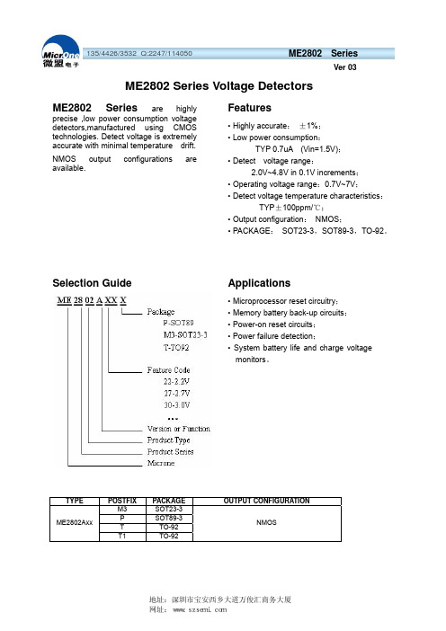
Ver 03TYPE POSTFIX PACKAGEOUTPUT CONFIGURATIONM3 SOT23-3 P SOT89-3T TO-92 ME2802AxxT1 TO-92NMOSME2802 Seriesare highlyprecise ,low power consumption voltage detectors,manufactured using CMOS technologies. Detect voltage is extremely accurate with minimal temperature drift.NMOS output configurations are available.• Microprocessor reset circuitry ; • Memory battery back-up circuits ; • Power-on reset circuits ; • Power failure detection ;• System battery life and charge voltage monitors 。
Features• Highly accurate : ±1%;• Low power consumption :TYP 0.7uA (Vin=1.5V);• Detect voltage range :2.0V~4.8V in 0.1V increments ; • Operating voltage range :0.7V~7V ;• Detect voltage temperature characteristics :TYP ±100ppm/℃;• Output configuration : NMOS ;• PACKAGE : SOT23-3,SOT89-3,TO-92。
ApplicationsME2802 Series Voltage Detectors Selection GuideVer 03 Pin ConfigurationPin AssignmentME2802AxxPIN NumberPINNAMEFUNCTIONSOT23-3 SOT89-3 TO-92(T)TO-92(T1)2 3 3 2 Vss Ground1 1 1 3 Vout Output3 2 2 1 Vin Input Block DiagramVer 03Absolute Maximum RatingsPARAMETER SYMBAL RATINGS UNITS V IN Input Voltage V IN 8 V Output Current Iout 50 mANMOS Vss-0.3~Vin+0.3Output Voltage N-ch open drain Vout Vss-0.3~12VSOT23 150 mW SOT89 500 mW Continuous TotalPower Dissipation TO92 Pd 300 mW Operating Ambient Temperature T Opr -40~+85 ℃Storage Temperature T stg -40~+125 ℃ Soldering temperature and time T solder 260℃, 10sElectrical Characteristics (V DF (T)=2.0V to 4.8V ±1% Ta=25℃)SYMBOL PARAMETER CONDITIONS MIN TYP MAX UNITS V DF Detect Voltage V DF * 0.99 V DFV DF *1.01V V HYSHysteresisRangeV DF *0.02 V DF * 0.05 V DF * 0.08 V0.7 2.7 0.8 3.2 0.9 3.6 1.0 3.8 Iss Supply Current Vin=1.5V =2.0V=3.0V=4.0V =5.0V 1.1 4.3 uAV INOperatingVoltageV DF (T)=1.6V to6.0V0.7 7 VI OUT Output CurrentN-ch VDS=0.5V VIN=1.0V=2.0V=3.0V =4.0V =5.0V1.0 3.0 5.0 6.0 7.02.2 7.7 10.1 11.5 13.0 mAΔV DF /(Δtopr*V DF ) Temperature characteristics -40℃≤Topr ≤ 85℃±100ppm/℃Note :1、VDF(T) :Established Detect Voltage value2、Release Voltage :V DR =V DF +V HYSVer 03Functional DescriptionTiming ChartDirections for useNotes on Use1、 Please use this IC within the stated maximum ratings. Operation beyond these limits may cause degradingor permanent damage to the device. 2、In order to stabilize the IC’s operations, please ensure that V IN pin’s input frequency’s rise and fall times aremore than several u Sec/V.Functional Description1、 When input voltage (V IN ) rises above detect voltage (V DF ), output voltage (V OUT ) will be equal to V IN .2、 When input voltage (V IN ) falls below detect voltage (VDF ), output voltage (V OUT ) will be equal to the ground voltage (V SS ) level.3、 When input voltage (V IN ) falls to a level below that of the minimum operating voltage (V MIN ), output will become unstable. In this condition, V IN will equal the pulled-up output ( should output be pulled-up.)4、 When input voltage (V IN ) rises above the ground voltage (V SS ) level, output will be unstable at levelsbelow the minimum operating voltage (V MIN ). Between the VMIN and detect release voltage (V DR ) levels, the ground voltage (V SS ) level will be maintained.5、 When input voltage (V IN ) rises above detect release voltage (V DR ), output voltage (V OUT ) will be equal toV IN .6、 The difference between V DR and V DF represents the hysteresis range.Ver 03 Typical ApplicationsType Characteristics1、SUPPLY CURRENT vs. INPUT VOLTAGEVer 03 2、DETECT,RELEASE VOLTAGE vs. AMBIENT TEMPERATURE3、OUTPUT VOLTAGE vs. INPUT VOLTAGEVer 03Ver 03 Package DiomensionsVer 03·The information described herein is subject to change without notice.·Nanjing Micro One Electronics Inc is not responsible for any problems caused by circuits or diagrams described herein whose related industrial properties, patents, or other rights belong to third parties. The application circuit examples explain typical applications of the products, and do not guarantee the success of any specific mass-production design.·Use of the information described herein for other purposes and/or reproduction or copying without the express permission of Nanjing Micro One Electronics Inc is strictly prohibited.·The products described herein cannot be used as part of any device or equipment affecting the human body, such as exercise equipment, medical equipment, security systems, gas equipment, or any apparatus installed in airplanes and other vehicles, without prior written permission of Nanjing Micro One Electronics Inc.·Although Nanjing Micro One Electronics Inc exerts the greatest possible effort to ensure high quality and reliability, the failure or malfunction of semiconductor products may occur. The user of these products should therefore give thorough consideration to safety design, including redundancy, fire-prevention measures, and malfunction prevention, to prevent any accidents, fires, or community damage that may ensue.。
常用小型稳压LDO等芯片推荐参考.
ME2111 17
ME2115 18
ME2206 19
ME2209 20 3.降压DC/DC转换器
ME3101 21
ME3102 22
ME3110 23 4.功率MOSFET
MEM2301 24
MEM2303 25
MEM2307 26
MEM2309 27
MEM2311 28
MEM2302 29
-输入电压:达6.5V
-输出电压范围:1.5V到5.0V
-最大输出电流:300mA(e.g.:Vin=4.3V,Vout=3.3V -低静态电流:8uA ( TYP.
-输入输出压差:200mV @100mA,400mV @ 200mA -高纹波抑制比:50dB(1KHz
-高精度:± 2%
-热关断保护
ME6211 500mA -6.5V 1.2-5V ±2% 50uA 75dB SOT-23-5LL/
SOT-89/DFN
量产
ME6219 300mA-6.5V 1.2-5V ±2% 65uA 62dB SOT-23-5LL量产ME1084 5A -25V 3.3-12V ±2% 5mA 50dB TO220/TO263 2009/Q3 ME1085 3A -25V 3.3-12V ±2% 5mA 50dB TO220/TO263 2009/Q3 ME1117 800mA -20V 1.25-12V ±2% 2mA 50dB SOT223/TO252 2009/Q2 ME3206 300mA -6.5V 1.2-5V ±2% 16uA 50dB SOT-23-5LL量产ME6401 200mA -6.5V 1.2-5V ±2% 130uA 62dB SOT-23-6LL量产
EMS208用户手册 V1.01

2 杭州远方仪器有限公司版权所有,未经许可不得复制和传播
EMS-208 半导体器件静电放电发生试仪器,为了确保您的人身安全和保护本仪器,务必注 意以下事项: 1. 2. 3. 4. 5. 6. 7. 本仪器的工作电源为AC100~240V,50Hz/60Hz。 仪器内有高压,切勿拆卸或敞开机壳工作。 当仪器有高压输出时,切勿触摸仪器的接线端子以及测试线,防止被电击。 在试验前须仔细检查连线,确保正确无误后方可进行试验。 为保证试验的正确性,配置试验时务必严格遵守相关测试标准要求。 测试前确保仪器的接地端良好接地。 请保持仪器清洁,为确保良好的通风散热,切勿堵塞机箱下盖板和后面板 上的通风孔,也勿放置障碍物,严禁覆盖。 8. 9. 仪器搬运时务必谨慎小心,防止碰撞、倒置、震动。 如发现表面较潮或存在污物,请马上停止操作,并做清理。
本用户手册及包括的任何资料, 其版权归远方公司所有, 受中华人民共和国 著作权法或国际相关法律保护。 未经本公司书面许可, 任何单位或个人不得以任 何方式或形式对本手册部分或全部内容进行复制、修改、传播、摘录、备份、翻 译成其他语言。 否则将构成对本公司著作权的侵犯, 侵权者将承担相关的法律后 果以及本公司的全部损失。 如果本公司与用户签有其他的书面协议, 且协议中涉及的本文档所含材料的 担保条款与上述条款有冲突,则该书面协议中的担保条款具有优先法律效力。
10. 测试完成后,保持相关设备运行一段时间,确保内部器件完全放电。 11. 当设置和更改连接其他设备时请切断发生器输出电源。 12. 正确使用探针说明及探针安放的角度,按探针上的箭头方向(“↑向上方向”) 把探针向上安置并且保持探针垂直(倾斜角度在 15°以内)。否则,可能会 引起电击或者难以操作发生器。 13. 操作时,不要碰触探针的放电端子部分,否则,可能会导致电击或者刺伤。 14. 请安全地把探针安装到探针平台上, 如果探针从平台上掉下来, 可能会损坏。 15. 请勿在发生器操作的时候更换探针,否则可能会导致电击造成严重的损坏。 16. 请勿把金属或者易燃物品放进部件、连接器及进气孔里面。 17. 请将仪器放在安全且易操作的地方,以免在紧急情况下难以操作仪器,导致 火灾或电击。 18. HBM、MM探针内部含有重金属汞,处理时请遵守当地相关法律。
2802说明书
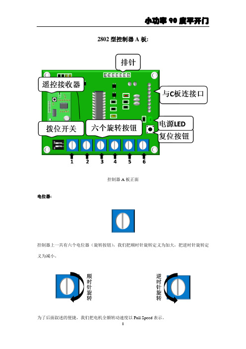
2802型控制器A板:控制器A板正面电位器:控制器上一共有六个电位器(旋转按钮),我们把顺时针旋转定义为加大,把逆时针旋转定义为减小。
为了后面叙述的便捷,我们把电机全额转动速度以Full Speed表示。
下面我们介绍每个电位器的功能。
1号电位器:控制快速开门速度,总共分为10挡具体数据:2号电位器:控制快速关门速度,总共分为10挡具体数据:3号电位器:控制缓冲速度,总共分为10挡具体数据:4号电位器:控制开门角度,总共分为10挡具体数据:5号电位器:控制开门到底的等待时间,总共分为10挡具体数据:4档14秒5档12秒6档10秒7档8秒8档6秒9档4秒10档2秒6号电位器:控制电机允许的电流(即扭距),总共分为10挡具体数据:档位允许电流1档1A2档 1.5A3档2A4档 2.5A5档3A6档 3.5A7档4A8档 4.5A9档5A10档 5.5A由于开关门速度,是由控制器控制电机运行所产生的。
为保护控制器免受过流过压的损害,电机的电压电流相互牵制,不让电机受损。
电源LED:电源指示灯,等灯光绿光闪亮的时候表明有外部电压进入,当外部电源断电或保险丝烧断,即指示灯熄灭。
复位按钮:当此按钮按下此按钮后,无论控制器处于什么状态,都将直接运行程序第一步。
拨位开关:此黑色插件为一个两位的拨位开关,拨位选项1,2共两个选项。
图片现在的位置为OFF状态,如需要开通某一功能,把其相对应的拨位开关向上拨到ON的位置。
其功能如下:1号拨位开关:顺/逆时针选择开关。
当1号拨位开关在OFF状态,为逆时针开启。
当2号拨位开关在ON状态,为顺时针开启。
2号拨位开关:每次/遥控上锁选择开关。
当2号拨位开关在OFF状态。
每次关门后自动上锁。
当2号拨位开关在ON状态,每次关门将不在上锁,只有遥控按钮按“止”当门关闭时,自动上锁。
排针:排针分排针头与排针座,排针头在线路A板,排针座在线路B板。
控制器为7芯排针,连接时需上下对齐。
遥控器如下图所示,遥控器一共有四个按钮,分别为“关”“常”“止”“开”。
TI PGA280 高精度仪表放大器数据手册说明书

ProductFolderOrderNowTechnicalDocumentsTools &SoftwareSupport &CommunityPGA280ZHCSL30B–JUNE2009–REVISED MARCH2020 PGA280零漂移、高电压、可编程增益仪表放大器1特性•宽输入电压范围:在±18V电源下,为±15.5V•二进制增益步长:128V/V至1/8V/V•额外比例缩放因子:1V/V和1⅜V/V•低失调电压:在G=128时为3μV•失调电压的近零长期漂移•近零增益温漂:0.5ppm/°C•出色的线性度:1.5ppm•出色的共模抑制比(CMRR):140dB•高输入阻抗•超低的1/f噪声•差分信号输出•过载检测•输入配置开关矩阵•断线测试电流•可扩展SPI™(具有校验和)•通用I/O端口•TSSOP-24封装2应用•模拟输入模块•数据采集(DAQ)•飞机发动机控制•电池测试3说明PGA280是一款高精度仪表放大器,具有数字控制增益和信号完整性测试功能。
该器件具有低失调电压,且失调电压、增益温漂和1/f噪声近乎为零,还具有出色的线性度、共模抑制比和电源抑制比,可支持高分辨率的精密测量。
36V电源电压和宽、高阻抗输入范围符合通用信号测量的要求。
特殊电路可防止多路复用器(MUX)开关产生浪涌电流。
另外,输入开关矩阵可实现在过载条件下轻松进行重新配置和系统级诊断。
可配置的通用输入/输出(GPIO)提供数种控制和通信功能。
SPI经扩展可与更多器件通信,仅需四个ISO耦合器即可实现隔离。
PGA280采用TSSOP-24封装,额定工作温度范围为–40°C至+105°C。
如需了解所有可用封装,请参阅数据表末尾的封装选项附录。
器件比较特性产品23位分辨率Δ-Σ模数转换器ADS1259斩波稳定仪表放大器,RR I/O,5V单电源INA333高精度PGA,G=1、10、100、1000PGA204高精度PGA,JFET输入,G=1、2、4、8PGA206典型应用PGA280ZHCSL30B–JUNE2009–REVISED 目录1特性 (1)2应用 (1)3说明 (1)4修订历史记录 (2)5Pin Configuration and Functions (3)6Specifications (4)6.1Absolute Maximum Ratings (4)6.2Electrical Characteristics (4)6.3Timing Requirements:Serial Interface (7)6.4Typical Characteristics (8)7Detailed Description (15)7.1Overview (15)7.2Functional Block Diagram (15)7.3Feature Description (16)7.4Device Functional Modes (24)7.5Programming (26)7.6Register Map (31)8Application and Implementation (38)8.1Application Information (38)9Power Supply Recommendations (39)10器件和文档支持 (41)10.1接收文档更新通知 (41)10.2支持资源 (41)10.3商标 (41)10.4静电放电警告 (41)10.5Glossary (41)11机械、封装和可订购信息 (41)4修订历史记录注:之前版本的页码可能与当前版本有所不同。
ET2670A耐压测试仪操作规程

ET2670A耐压测试仪操作规程一、设备介绍二、设备结构及工作原理1.设备结构2.工作原理三、操作步骤1.安全操作(1)在操作前,确认设备的电源已接地并符合安全要求。
(2)使用前,请先关闭设备的电源开关,确保设备处于停机状态。
(3)在使用设备前,请戴好绝缘手套,确保人身安全。
2.设备准备(1)检查设备的电源线是否完好,电源插座是否与电网连接稳定。
(2)检查高压输出终端是否良好连接、无松动现象。
(3)检查设备的控制面板是否完好,并确保控制按钮可以正常操作。
(4)将被测试绝缘材料或电器设备连接到设备的高压输出终端。
3.设备操作(1)打开设备的电源开关,设备进入工作状态。
(2)通过设备的控制面板设置预定电压值,并选择测试持续时间。
(3)按下“开始测试”按钮,设备开始向被测试物体施加高电压。
(4)设备会自动检测被测试物体是否出现击穿或漏电现象,并记录测试结果。
(5)测试完成后,设备会自动停止输出高电压。
将被测试物体与设备的高压输出终端分离。
4.数据记录(1)测试过程中设备会自动记录被测试物体是否出现击穿或漏电现象。
(2)测试完成后,设备可以通过USB接口将测试数据导出到计算机或打印机进行保存。
四、设备维护1.设备定期维护(1)每月对设备进行一次全面检查,包括检查电源线、插座、控制面板等是否完好。
(2)定期检查设备的高压输出终端是否有松动现象,确保其连接正常稳固。
(3)定期清理设备外部灰尘,保持设备的通风良好。
2.设备故障处理(1)在设备故障时,请关闭设备的电源开关,并在没有电源的情况下进行维修。
以上为ET2670A耐压测试仪的操作规程,希望能对操作人员有所帮助。
在操作过程中,请务必注意安全,并按照规程进行操作,以保障设备的正常运行和人身安全。
ME2805型号高精度电压检测器说明书

ME2805Ultra-small package High-precision Voltage Detector with delaycircuit, ME2805 SeriesGeneral Description FeaturesME2805 Series is a series of high-precision voltage detectors with a built-in delay time generator of fixed time developed using CMOS process. Internal oscillator and counter timer can delay the release signal without external parts. Detect voltage is extremely accurate with minimal temperature drift. CMOS output configurations are available. ● Highly accuracy : ±1%● Low power consumption :TYP 0.9uA (V DD =3V) ● Detect voltage range :1.0V~6.5V in 0.1Vincrements● Operating voltage range :0.7V~7V● Detect voltage temperature characteristics :TYP±100ppm/℃● Output configuration : CMOSTypical Application● Power monitor for portable equipment such as notebook computers, digital still cameras, PDA, and cellular phones● Constant voltage power monitor for cameras, videoequipmentandcommunicationdevices.● Power monitor for microcomputers and resetfor CPUs.● System battery life and charge voltagemonitorsTypical Application CircuitPackage● 3-pin SOT23-3、SOT23Selection GuideME 2805X X GEnvironment markPackage:X Function Product Type Product Series MicroneX X Output Voltage X-SOT23M3-SOT23-3NOTE: If you need other voltage and package, please contact our sales staff.product series product descriptionME2805A263M3G V OUT =2.63V ;Rising edge detection ;Package :SOT23-3 ME2805A263XG V OUT =2.63V ;Rising edge detection ;Package :SOT23 ME2805A293M3G V OUT =2.93V ;Rising edge detection ;Package :SOT23-3 ME2805A293XG V OUT =2.93V ;Rising edge detection ;Package :SOT23 ME2805A308XGV OUT =3.08V ;Rising edge detection ;Package :SOT23 ME2805A463XG V OUT =4.63V ;Rising edge detection ;Package :SOT23Pin Configuration123123SOT-23SOT-23-3Pin AssignmentPIN Number Pin Name Function SOT-23-3/SOT-231 VSS Ground2 VOUT Output Voltage 3VDDInput VoltageBlock DiagramAbsolute Maximum RatingsPARAMETER SYMBAL RATINGSUNITS V IN Input Voltage V IN 8 V Output CurrentI OUT 50mA Output Voltage CMOS V OUT GND-0.3~V IN +0.3V Continuous Total PowerDissipationSOT-23-3 Pd 300 mW SOT-23250 Operating Ambient TemperatureT Opr -40~+85 ℃ Storage Temperature T stg -40~+125 ℃ Soldering temperature and timeT solder 260℃, 10sESDMM 400 V HBM4000VElectrical Characteristics(-V DET(S)=1.0V to 6.5V±2% ,Ta=25O C , unless otherwise noted)Parameter Symbol Conditions Min. Typ Max.UnitsTest circuitDetect Voltage (Output Voltage)-VDET --VDET(S)×0.99-VDET(S)-VDET(S)×1.01V1 HysteresisRangeVHYS - 0.03 0.06 0.1 VSupply Current ISSVDD=3V (below 2.5V) - 0.9 1.5uA2VDD=5V (2.5V-4.5V) - 1.4 2.8VDD=7V (4.5V-6.5V) - 1.8 3.6Output CurrentIoutN-chVDS=0.5V VDD=0.7V 0.01 0.19 --mA3IoutP-ch VDS=0.5V VDD=7V 1.7 3.4 --mA4OperatingvoltageVDD - 0.7 - 7 V 1 Delay timeTd1 VDD=-VDET+1V DS low 130 200 290 ms 1Td2 VDD=-VDET+1V DS high 110 220 330 us 5 Temperaturecharacteristics VDETTaVDET-∙∆-∆Ta∆=-40℃~ 85℃- ±100 ±350 ppm/℃ 1 Note:1、-VDET(S) :Specified Detection Voltage value2、-VDET :Actual Detection Voltage value3、Release Voltage:+VDET=-VDET+VHYSTest Circuits:1. 2.3. 4.5.Functional Description :1. Basic Operation: CMOS Output (Active Low)1-1. When the power supply voltage (VDD) is higher than the release voltage (+VDET), the Nch transistor is OFF andthe Pch transistor is ON to provide VDD (high) at the output. Since the Nch transistor N1 in Figure 1 is OFF, thecomparator input voltage isC B A C B R R R VDD R R ++∙+)(.1-2. When the VDD goes below +VDET, the output provides the VDD level, as long as VDD remains above thedetection voltage (–VDET). When the VDD falls below –VDET (point A in Figure 2), the Nch transistor becomes ON, the Pch transistor becomes OFF, and the VSS level appears at the output. At this time the Nchtransistor N1 in Figure 1 becomes ON, the comparator input voltage is changed to B AB R R VDD R +∙.1-3. When the VDD falls below the minimum operating voltage, the output becomes undefined, or goes to VDD whenthe output is pulled up to VDD.1-4. The VSS level appears when VDD rises above the minimum operating voltage. The VSS level still appearseven when VDD surpasses the –VDET, as long as it does not exceed the release voltage +VDET.1-5. When VDD rises above +VDET (point B in Figure 2), the Nch transistor becomes OFF and the Pch transistorbecomes ON to provide VDD at the output. The VDD at the OUT pin is delayed for Td due to the delay circuit.2. Delay Circuit2-1. Delay TimeThe delay circuit delays the output signal from the time at which the power voltage (VDD) exceeds the release voltage (+VDET) when VDD is turned on. The output signal is not delayed when the VDD goes below the detection voltage (–VDET). (Refer to Figure 2.) The delay time (t D) is a fixed value that is determined by a built-in oscillation circuit and counter.2-2. DS Pin (ON/OFF Switch Pin for Delay Time)The DS pin should be connected to Low or High. When the DS pin is High, the output delay time becomes short since the output signal is taken from the middle of counter circuit (Refer to Figure 3).Directions for use:1、Please use this IC within the stated maximum ratings. Operation beyond these limits may cause degrading orpermanent damage to the device.2、When a resistor is connected between the V DD pin and the input with CMOS output configurations, oscillation mayoccur as a result of voltage drops at R IN if load current(I OUT) exists.(refer to the Oscillation Description(1) below)3、When a resistor is connected between the V DD pin and the input with CMOS output configurations, oscillation mayoccur as a result of through current at the time of voltage release even if load current(I OUT) does not exist. (refer to the Oscillation Description(2) below)4、With a resistor connected between the V DD and the input, detect and release voltage will rise as a result of the IC’ssupply current flowing through the V DD pin.5、In order to stabilize the IC’s operations, please ensure that V DD pin’s input frequency’s rise and fall times are morethan several u Sec/V.Oscillation Description:1、 Output current oscillation with the CMOS output configurationWhen the voltage applied at IN rises, release operations commence and the detector’s output voltage increase.Load current(I OUT) will flow at R L. Because a voltage drop(R IN*I OUT) is produces at the R IN resistor, located between the input(IN) and the V DD pin. The load current will flow via the IC’s pin. The voltage drop will also lead toa fall in the voltage level at the V DD pin. When the V DD pin voltage level falls below the detect voltage level, detectoperations will commence. Fllowing detect operations, load current flow will cease and since voltage drop at R IN will disapper, the voltage level at the V DD pin will rise and release operations will begin over again. Oscillation may occur with this “release-detect-release” repetition. Further, this condition will also appear via means of a similar mechanism during detect operations.2、 Oscillation as a result of through currentSince the ME2805 series are CMOS IC’s, through current will flow when the IC’s internal circuit switching operates(during release and detect operations). Consequently, oscillation is liable to occur as a result of drops in voltage at the through current’s resistor(R IN) during release voltage operations.(refer to diagram 2) since hysteresis exists during detect operations, oscillation is unlikely to occur.Type Characteristics1、SUPPLY CURRENT VS. AMBIENT TEMPERATUREVDD=5V,-VDET=2.63V VDD=2.5V,-VDET=2.63VIss VS.TEMP0.30.60.91.21.51.82.12.42.7-16102030405060708090100110120TEMP(℃)I s s (u A )Iss VS.TEMP0.20.40.60.811.2-16102030405060708090100110120TEMP(℃)I s s (u A )2、SUPPLY CURRENT VS. INPUT VOLTAGE3、DETECT,RELEASE VOLTAGE VS. AMBIENTTEMPERATURE-VDET=2.63V (T=25℃) -VDET=2.63VIss VS VDD0.511.522.500.511.52 2.53 3.54 4.55 5.566.577.5VDD(V)I s s (u A )VDET VS TEMP2.542.562.582.62.622.642.662.682.72.72-16102030405060708090100110120TEMP(℃)V D E T (V )-VDET +VDE T4、 OUTPUT CURRENT VS. INPUT VOLTAGEN-ch VDS=0.5V,-VDET=2.63V P-ch VDS=0.5V,-VDET=2.63VIout(N) VS. VDD0246810120.20.50.71 1.2 1.7 2.2 2.5VDD(V)I o u t (m A )T=85℃T=-15℃T=23℃I o u t (P ) V S. V00.511.522.533.542.73.2 3.544.555.56V D D (V )I o u t (mT =-15℃T =23℃T =85℃Packaging Information● SOT23DIMMillimetersInchesMinMax Min Max A 0.9 1.2 0.0354 0.0472 A1 0 0.14 0.0000 0.0055 A2 0.9 1.05 0.0354 0.0413 b 0.28 0.52 0.0110 0.0205 c 0.07 0.23 0.0028 0.0091 D 2.8 3.0 0.1102 0.1181 e1 1.8 2.0 0.0709 0.0787 E 1.2 1.4 0.0472 0.0551 E1 2.22.60.08660.1024e 0.95(TYP) 0.0374(TYP) L 0.55(TYP)0.0217(TYP)L1 0.25 0.55 0.0098 0.0217θ 08° 0.00008°c10.25(TYP)0.0098(TYP)● SOT23-3DIMMillimetersInchesMinMax Min Max A 0.9 1.2 0.0354 0.0472 A1 0 0.14 0.0000 0.0055 A2 0.9 1.05 0.0354 0.0413 b 0.28 0.52 0.0110 0.0205 c 0.07 0.23 0.0028 0.0091 D 2.8 3.0 0.1102 0.1181 e1 1.8 2.0 0.0709 0.0787 E 1.2 1.4 0.0472 0.0551 E1 2.22.60.08660.1024e 0.95(TYP) 0.0374(TYP) L 0.55(TYP)0.0217(TYP)L1 0.25 0.55 0.0098 0.0217 θ 08° 0.00008°c1 0.25(TYP)0.0098(TYP)V04 Page 11 of 11 ME2805● The information described herein is subject to change without notice.● Nanjing Micro One Electronics Inc is not responsible for any problems caused by circuits or diagrams described herein whose related industrial properties, patents, or other rights belong to third parties. The application circuit examples explain typical applications of the products, and do not guarantee the success of any specific mass-production design.● Use of the information described herein for other purposes and/or reproduction or copying without the express permission of Nanjing Micro One Electronics Inc is strictly prohibited.● The products described herein cannot be used as part of any device or equipment affecting the human body, such as exercise equipment, medical equipment, security systems, gas equipment, or any apparatus installed in airplanes and other vehicles, without prior written permission of Nanjing Micro One Electronics Inc.● Although Nanjing Micro One Electronics Inc exerts the greatest possible effort to ensure high quality and reliability, the failure or malfunction of semiconductor products may occur. The user of these products should therefore give thorough consideration to safety design, including redundancy, fire-prevention measures, and malfunction prevention, to prevent any accidents, fires, or community damage that may ensue.。
ME8320 原边控制芯片

典型应用图
ME8320
C1 R1
T1
D6
Np
Ns
C3
深圳市国兴顺电子有限公司 R4 D5 R3 C2 Na
R2 MOS
ME8320
Rs
图.1 5V1A充电器系统应用图
深圳市国兴顺电子有限公司
QQ:514789807 手机:13926511192
Page 2 of 12
选购指南 芯片脚位图
ME8320
最大线损补偿电流
电流检测部分 (CS 管脚)
CS前沿消隐时间
芯片关断延迟
CL=1nF at GATE
恒流控制部分 (CC管脚)
内部CC基准电压
栅极驱动输出(GATE管脚)
输出低电平
Io=20mA(sink)
输出高电平
Io=20mA(source)
输出钳位电压
VDD=24V
输出上升时间
CL=0.5nF
尺寸(mm)
最小值
最大值
0.9
1.45
0
0.15
0.9
1.3
0.2
0.5
0.09
0.26
2.7
3.10
2.2
3.2
1.30
1.80
0.95REF
1.90REF
0.10 00
0.60 300
最小值 0.0354
0 0.0354 0.0078 0.0035 0.1062 0.0866 0.0511
0.0039 00
输出下降时间
CL=0.5nF
过热保护温度
14 15.5 16.5 V 31 33 35 V 33 35 37 V
1.98 2.0 2.02 V
- 1、下载文档前请自行甄别文档内容的完整性,平台不提供额外的编辑、内容补充、找答案等附加服务。
- 2、"仅部分预览"的文档,不可在线预览部分如存在完整性等问题,可反馈申请退款(可完整预览的文档不适用该条件!)。
- 3、如文档侵犯您的权益,请联系客服反馈,我们会尽快为您处理(人工客服工作时间:9:00-18:30)。
Ver 03
TYPE POSTFIX PACKAGE
OUTPUT CONFIGURATION
M3 SOT23-3 P SOT89-3
T TO-92 ME2802Axx
T1 TO-92
NMOS
ME2802 Series
are highly
precise ,low power consumption voltage detectors,manufactured using CMOS technologies. Detect voltage is extremely accurate with minimal temperature drift.NMOS output configurations are available.
• Microprocessor reset circuitry ; • Memory battery back-up circuits ; • Power-on reset circuits ; • Power failure detection ;
• System battery life and charge voltage monitors 。
Features
• Highly accurate : ±1%;
• Low power consumption :
TYP 0.7uA (Vin=1.5V);
• Detect voltage range :
2.0V~4.8V in 0.1V increments ; • Operating voltage range :0.7V~7V ;
• Detect voltage temperature characteristics :
TYP ±100ppm/℃;
• Output configuration : NMOS ;
• PACKAGE : SOT23-3,SOT89-3,TO-92。
Applications
ME2802 Series Voltage Detectors Selection Guide
Ver 03 Pin Configuration
Pin Assignment
ME2802Axx
PIN Number
PIN
NAME
FUNCTION
SOT23-3 SOT89-3 TO-92(T)TO-92(T1)
2 3 3 2 Vss Ground
1 1 1 3 Vout Output
3 2 2 1 Vin Input Block Diagram
Ver 03
Absolute Maximum Ratings
PARAMETER SYMBAL RATINGS UNITS V IN Input Voltage V IN 8 V Output Current Iout 50 mA
NMOS Vss-0.3~Vin+0.3
Output Voltage N-ch open drain Vout Vss-0.3~12
V
SOT23 150 mW SOT89 500 mW Continuous Total
Power Dissipation TO92 Pd 300 mW Operating Ambient Temperature T Opr -40~+85 ℃
Storage Temperature T stg -40~+125 ℃ Soldering temperature and time T solder 260℃, 10s
Electrical Characteristics (V DF (T)=2.0V to 4.8V ±1% Ta=25℃)
SYMBOL PARAMETER CONDITIONS MIN TYP MAX UNITS V DF Detect Voltage V DF * 0.99 V DF
V DF *
1.01
V V HYS
Hysteresis
Range
V DF *
0.02 V DF * 0.05 V DF * 0.08 V
0.7 2.7 0.8 3.2 0.9 3.6 1.0 3.8 Iss Supply Current Vin=1.5V =2.0V
=3.0V
=4.0V =5.0V 1.1 4.3 uA
V IN
Operating
Voltage
V DF (T)=1.6V to
6.0V
0.7 7 V
I OUT Output Current
N-ch VDS=0.5V VIN=1.0V
=2.0V
=3.0V =4.0V =5.0V
1.0 3.0 5.0 6.0 7.0
2.2 7.7 10.1 11.5 1
3.0 mA
ΔV DF /(
Δtopr*V DF ) Temperature characteristics -40℃≤Topr ≤ 85℃
±100
ppm/℃
Note :1、VDF(T) :Established Detect Voltage value
2、Release Voltage :V DR =V DF +V HYS
Ver 03
Functional Description
Timing Chart
Directions for use
Notes on Use
1、 Please use this IC within the stated maximum ratings. Operation beyond these limits may cause degrading
or permanent damage to the device. 2、In order to stabilize the IC’s operations, please ensure that V IN pin’s input frequency’s rise and fall times are
more than several u Sec/V.
Functional Description
1、 When input voltage (V IN ) rises above detect voltage (V DF ), output voltage (V OUT ) will be equal to V IN .
2、 When input voltage (V IN ) falls below detect voltage (V
DF ), output voltage (V OUT ) will be equal to the ground voltage (V SS ) level.
3、 When input voltage (V IN ) falls to a level below that of the minimum operating voltage (V MIN ), output will become unstable. In this condition, V IN will equal the pulled-up output ( should output be pulled-up.)
4、 When input voltage (V IN ) rises above the ground voltage (V SS ) level, output will be unstable at levels
below the minimum operating voltage (V MIN ). Between the VMIN and detect release voltage (V DR ) levels, the ground voltage (V SS ) level will be maintained.
5、 When input voltage (V IN ) rises above detect release voltage (V DR ), output voltage (V OUT ) will be equal to
V IN .
6、 The difference between V DR and V DF represents the hysteresis range.
Ver 03 Typical Applications
Type Characteristics
1、SUPPLY CURRENT vs. INPUT VOLTAGE
Ver 03 2、DETECT,RELEASE VOLTAGE vs. AMBIENT TEMPERATURE
3、OUTPUT VOLTAGE vs. INPUT VOLTAGE
Ver 03
Ver 03 Package Diomensions。