台湾CCT承认书,CCT电容规格书
NEC钽电容规格书
Z
Z
Z
Z
Unit : mm (inch)
L
W1
W2
H
Z
1.6 ± 0.1 (0.061±0.004)
PDF 文件使用 "pdfFactory Pro" 试用版本创建
Correct Use of NeoCapacitor (Please Read)
[Notes] l Be sure to read "Notes on Using The NeoCapacitor" (p29 - p32) and "Cautions" (p35) before
Packaging ………………………………………………………………………………… 27
Notes on Using The NeoCapacitor …………………………………………………… 29
PDF 文件使用 "pdfFactory Pro" 试用版本创建
What's NeoCapacitor
2.2 to 1000
±20
330 to 680
±20
DC Leakage Current ( A)
0.1 CV or 3, (J case, 10 A) whichever greater
0.1 CV or 3, whichever greater
Dissipation Factor (%)
4 to 10
Dimensions
J, P, A2 and A case
L
W1
B3, B2 and V case
L
W1
C2, C and D case
L
W1
CC1瓷片电容规格书
d 10%
F 0.8 0.2
d 10%
F 0.8 0.2
d 10%
(b )
编带产品
2.5max 11max
2.5max 17min
2.5max
引脚距离和引线形式常规按EIA和JIS的标准执行。同时我们可以根据客户要求,做出符合客户使用习惯的引脚距离和引线形式。 NOTE: Lead style and distance are fit of JIS and EIA standard. Other we can produce with customers requirement.
1 15 1 30 22 50 47 68 70 82 86 100 100 120 120 150 ------
5 68 10 100 70 150 82 180 100 200 160 220 200 260 270 330 330 560
1 120 30 150 150 220 180 250 240 330 360 470 500 560 600 680 820 1000
8 容量允许偏差见EIA代码表: Capacitance tolerance, Please consider EIA code
代码
J
K
M
误差
S
Z
9 包装形式 Packing style 代码 symbol
T S
包装形式 盒带包装
散包装
Packing style Tape bulk
10 包封形式 Enclosure style 代码 code
E P
包封形式 环氧包封 酚醛包封
Enciosure style Epoxy resin Phenol resin
台湾信昌 MLCC(多层瓷介电容)推介资料

PDC -MLCC ProductsAS 9100C Aerospace Quality Management System航太品質管理系統認證TS 16949 Automotive Quality Management System汽車品質管理系統認證UL Safety Certified 安規認證Portfolios Series Size Dielectric Rating Volt CapacitanceGeneral Purpose FN Series0402 to 1812NPO/X7RX5R/Y5V≦100V≦0.82uFHigh Cap Mini-Volt.FS Series0402 to 1812X7R/X5RY5V≦50V1uF to 100uFHigh Cap Mid-Volt.FS Series1206 to 2225X7R50V to 100V0.68uF-10uF Middle Voltage FM Series0603 to 2225NPO/X7R≧100V to 630V≦1uFHigh Voltage FV Series1808/2211/2220NPO/X7R≧1000V≦68nF Safety Certificated FH & FK Series1206 to 2211NPO/X7R AC 250V≦4.7nF Military standard FM Series0603 to 2225NPO/X7R25V to 1000V Full range High Freq.RF & HH Series0201/0402NPO50V/100V≦1nFBig Size FG Series≧2220NPO/X7R25 to 3000V Full range Low D.F.FL Series Full range X7R250V/500V≦3.3nFSoft Terminal MLCC FP Series0805 up X7R≧100V to 3000V Full rangeMLCC Products≤630V≤50V10,000VAEC Q200High Cap1uF330uFH i g h V o lMEGA CAPM I L -S T DH i g h Q /R F /H CMid-Vol & High CapPDC MLCC Product Series MapSafety Certified MLCCSafety Capacitor Applications (X1/Y2 & X2)X1/Y2: TUV EN132400X2: TUV EN132400, UL60950Applications:Designed for AC surge and lightning protection in line-to-ground interface.1.Switching Power Supply2.Modems/ADSL/VOIP Ethernet Protection.(3KV~5KV/ AC250V)3.Computer networks.(3KV~5KV/AC250V)FH08X151K302EProduct Code FH:X2FK:X1Y2Chip Size 08:180812:181211:2211Dielectric N: NPO X: X7RCapacitance 151:15*101PFTolerance J : +/-5%K : +/-10%Rated Voltage X2Y3:302X1Y2:502Packaging E:EmbossedThickness E:1.65mm F:2.00mm G:2.50mmSpecial CodeG:Pb/Cd freeFGX1/Y2 X2AC Capacitors(Safety Capacitor ; X1/Y2 ;X2/Y3)IEC 60950(Telecom applications) T1=10us T2=700us IEC 60384-14(Power applications) T1=1.2us T2=50usRating Rated Voltage Vac Dielectric Withstanding Voltage Impulse Voltage Y2250Vac 1500Vac at 60Hz 5000V X1250Vac 1500Vac at 60Hz 4000V X2250Vac1500Vac at 60Hz2500VSeries Description WorkingVoltageImpulseVoltageT.C.C1808181222112220FK X1/Y2 Safety certified CapacitorUL/TUV(X1/Y2安規電容)AC250V5KVNPO271471721X7R102102222472FH X2 Safety certified CapacitorUL/TUV(X2安規電容)AC250V 2.5KVNPO102102X7R222562Interface Safety certified CapacitorSeries Description WorkingVoltageT.C.C120612101808181218252020221122202225FV High VoltageMLCC1000V-6000V(高壓電容)1KVNP0681102152222332332332332392X7R103103123473683683104104104 2KVNP0271561102122152152152152182X7R222222222472682682822822103 3KVNP0680221331471102102102102122X7R102182222222272272332 4KVNP0121221471471471471561X7R561821102102122122152 5KVNP0271331331471X7R821821102102 6KVNP0101101121151X7R681681821821FP Series Soft Termination MLCCCap Max .06030805120612101808181218252220222550V 104224105475335106106106100V 333224105225335106106106200V/250V 103333104684105225225275500V 223333124224684684105630V 2233331242246846841051KV 2233332735631041241542KV 2225625621032732733333KV222472123123153SizeRated VoltageThe capacitance listed in this table is the maximum available capacitance.FP Series Soft Termination MLCC•High performance to withstand 5mm bending test guarantee.PDC FP series is added a special termination material (Ultra-Buffer)between ceramic body and Ni-barrier that can absorb mechanical stress to prevent bending crack occurred.100% Sn External TerminaitonInner ElectrodeCu TerminationUltra-Buffer (Epoxy)Ni-barrier100% Sn External TerminaitonPDC FP Series solve risk of bending crack structureSoft termination products cross referencePDCMurataYageoSamsungTerminationInner layer Cu CuCu CuMiddle 1stlayerUltra-BufferConductive Cu polymerSoft electrodeSoft termination Flexible layerMiddle 2nd layer Ni Ni Ni Ni Outer layerSn SnSn Sn Coding rule(eg.0805)FP 21******GRJ 21**** / GCJ 21****CS 0805****CL*********4***/CL *********5***Bending Spec >=5mm >=3mm >=3mm Class Ⅰ:3mm; Class Ⅱ:2mmDielectric NP0/X7R X7R X7R C0G/X7R Size 0603~22250603~22200603~12060402~1206Rated Voltage 50V~3000V 10V~1000V 16V~630V 10V~100V Capacitance100pF~10uF1000pF~10uF100pF~1uF100pF~22uFFV Series Arc Prevention MLCCArc Prevention MLCCElectric ArcSurface CoatingChip Size1206180822112220 Voltage50V to 5000VDielectric Class II / Class IProduct rangeFE Series High Reliability Mega CapNo Part Material 1Ceramic DielectricBaTiO 32ElectrodeNi 3TerminationCu 4Ni 5Sn 6Joint High Temperatue Solder(Pb free)7Metal Lead Frame Cu AlloyMeg Cap Products SeriesHigh Reliability ProductsHigher Capacitance as same mounting area121018122220 / 1825 / 2225Stacked Chip Number CapacitanceStacked ChipNumberCapacitanceStacked ChipNumberCapacitance11time11time11time2 2 time2 2 time2 2 time3 3 time4 4 time More stacked chip number, more higher capacitance.Higher Capacitance as same mounting area1210181222201 stacked2 stacked 1 stacked 2 stacked 1 stacked 2 stacked3 stacked4 stacked TDK◎◎◎◎◎Murata◎◎◎◎◎PDC◎◎◎◎◎◎◎◎PDC could support higher capacitance products.Mega Cap Products SeriesFeature of each CapacitorsNormal MLCC Mega Cap Ta Cap ShapePolarity no no yes Bending Strength good excellent excellent Voltage Proof excellent excellent Bad ESR excellent excellent Bad Reliability good excellent BadPrice excellent good ExcellentMG/MT Series Automotive MLCCReliability AEC-Q200 QualifiedGrade 1Non AEC-Q200 qualifiedMost passenger compartmentGeneral Purpose MLCCNon AutomotiveStandard series(General purpose)MG / OP / SH / SGRF / HHMT / MY (array)RT / STMLCC series Automotive ApplicationDielectric NP0X7R X5RSize0402, 0603, 0805, 1206, 1210, 1812Capacitance range0.5pF to 0.033uF100pF to 2.2uF0.056uF to 10uF Rated voltage (WVDC)10V~630V 6.3V ~ 250V 6.3V, 10V, 16V, 25V Operating temperature-55 to +125°C-55 to +85°C Capacitance characteristic±30ppm/°C±15%Termination Ni/Sn (lead-free termination)MG series MLCC (Non AEC-Q200 series)MT series MLCC (AEC-Q200 Qualified series)Dielectric X7R NP0Range Size Rated voltage Capacitance range Size Rated voltage Capacitance range 040210~50V100~10nF040210V ~ 50V0.5pF ~ 1000pF060310~50V100pF~100nF060310V ~ 100V0.5pF ~ 1000pF 100V100pF~10nF200V0.5pF~100pF 080510~630V~1uF(25V), ~220nF(50V),~0.1uF(100V),~22nF(250V), ~10nF(630V)080510~50V0.5pF~ 4.7nF100V0.5pF~1nF 120610~50V220pF~1uF120610~100V 1.2pF~10nF100~630V220pF~220nF(100V)~22nF(250V), ~10nF(630V)200~630V 1.2pF~2.2nF1210250V10pF~3.9nFOperating temperature-55 to +125°C Standard series of Automotive MLCCRF Series Hi-Frequency MLCCFEATURES1.Made by BME technology with Cu inner electrodes.2.Excellent Q level at high frequency applications.3.Having high SRF characteristic.4.Offer ultra low capacitance to 0.1pF.5.Offer high precision capacitance tolerance to ±0.05pF6. Lead-free and Meet RoHSAPPLICATIONS1.Mobile phones and telecommunication equipments.2.Related to satellite equipments and products.3.RF Modules: Power amplifier, VCO.PDC’s RF03N-MLCC applied in WiFi 802.11 a/b/g/n/ac/ad module Dielectric NP0 characteristic Size Ultra-small : 01005Regular : 0201, 0402, 0603, 0805Square : 0505, 1111Rated voltage (WVDC)01005 : 16V/25V (New launch)0201 : 6.3V ~ 50V0402 : 50V ~ 200V0603 : 50V ~ 250V0805 : 50V ~ 500V0505 : 50V ~ 250V1111: 500V (New launch)PDC RF-series MLCCPDC classifies & provides different Q level of NPO-MLCCs fordifferent application fields and competitive prices .High Q / Low ESR MLCCs in Market RF-Series GJM/GQ M Series S-series ATC600HH-SeriesNormal NPO C-series L-series H i g h Q ATCGRMSeriesNormalwith Cu inner-electrode with Ag inner-electrodeATC800ATC100MLCC OEM/ODM SolutionsMLCC Big size Product MAP Rated Voltage50V100V200V/250V500V/630VDielectric X7R X7R X7R X7R 1210475225474563 1812275225105124 1825565475225334 2020565475225334 2220685475225474 2225685475225105 3035685475335125 3333825475335125 3530825475475125 3640825565475225 3940825655565225 4045106685565225 4238106685565335 4252106685685335* We also can provide customer made product range , please contact with PDC local representative.Application of CircuitFunction Product Type Capacitance Voltage Size MaterialSmoothing Low Volt.1uF ~100uF 3.3V/6.3V/10V/16V≦1206X7R/X5R Mid Volt.1uF~22uF25/50V≧1206X7R High Volt.0.1uF~4.7uF100V/250V/500V/1KV≧1206X7RDe-coupling High Volt.1p~33pF3000/5000/6000V≧1808NPOOscillation Low Vol.0.1nF~22nF10V/16V≦0805NPO High Vol.1nF~10nF250V/500V≧1210NPOSnubber High Voltage1nF~10nF100/250/500/1000V≧0805X7R Tuning High Freq.0.1p~1nF50V/100V≦0603NPOInterface High Volt.0.68~2.2nF2000V/3000V≧1206X7R Safety Cap0.68~2.2nF AC 250V≧1206X7RApplication of CircuitFunction Product Type Capacitance Voltage Size MaterialSmoothing 平滑電路FS Series1uF ~330uF 3.3V to 25V≦1206X7R/X5R FM/FS Series0.1uF~4.7uF100V/250V/500V≧1206X7REMI(De)Coupling (去)偶合FM/FV Series0.1nF~10nF250V/630V/1000V/3000V≧0805NPO/X7ROscillation振盪電路FM Series1nF~10nF250V/500V≧1210NPOSnubber 緩衝電路FM/FV Series1nF~10nF100/250/500/1000V≧0805X7RApplication of Power Circuit電源電路應用Smoothing Circuit (平滑電路)Series Description WorkingVoltageT.C.C120612101808181218252020221122202225FS Smoothing Function Capacitor≧50v ,1uF(濾波電容)50VX7R475225275565565685685X5R475106106100V X7R105225225475475475475200/250V X7R105225225225225FG Big size MLCC(大尺寸電容)50-10KV X7RChip Size 3035 to 13060 , Capacitance Please contactwith PDCEMI (De)Coupling Circuit/(去)偶合電路Series Description WorkingVoltageT.C.C120612101808181218252020221122202225FV High VoltageMLCC1000V-6000V(高壓電容)1KVNP0681102152222332332332332392X7R103103123473683683104104104 2KVNP0271561102122152152152152182X7R222222222472682682822822103 3KVNP0680221331471102102102102122X7R102182222222272272332 4KVNP0121221471471471471561X7R561821102102122122152 5KVNP0271331331471X7R821821102102 6KVNP0101101121151X7R681681821821L/C Oscillation Circuit 電感電容振盪電路Series Description WorkingVoltageT.C.C121018121825202022202225FM Middle Voltage MLCC100V-630V(中電壓電容)250V NPO392682822822822103500V NPO182332472472472682FL Low Dissipation MLCC(低損型電容)250V X7E154684500V X7E473Snubber circuit (緩衝電路)Series Description WorkingVoltageT.C.C0805120612101808181222112220FM Middle Voltage MLCC100V-630V(中電壓電容)250VNPO102222392682822X7R333104474105225 500VNPO391222182332472X7R223333563124474FV High Voltage MLCC1000V-6000V(高壓電容)1KVNP0681102152222332332X7R103103123473104104 2KVNP0271561102122152152X7R222222222472822822 3KVNP0680221331471102102X7R102182272272Series Description WorkingVoltageImpulseVoltageT.C.C1808181222112220FK X1/Y2 Safety certified CapacitorUL/TUV(X1/Y2安規電容)AC250V5KVNPO271471721X7R102102222472FH X2 Safety certified CapacitorUL/TUV(X2安規電容)AC250V 2.5KVNPO102102X7R222562Interface Safety certified CapacitorSeries Description WorkingVoltageT.C.C120612101808181218252020221122202225FV High VoltageMLCC1000V-6000V(高壓電容)1KVNP0681102152222332332332332392X7R103103123473683683104104104 2KVNP0271561102122152152152152182X7R222222222472682682822822103 3KVNP0680221331471102102102102122X7R102182222222272272332 4KVNP0121221471471471471561X7R561821102102122122152 5KVNP0271331331471X7R821821102102 6KVNP0101101121151X7R681681821821Thank You。
国巨电容规格书
CC 0805 K K X7R 9 B N 104
Code 1~2 Series Name CC = Multi-layer
chip cap. CA = Cap. Array CL=Low. Inductance
Code 3~6
Size Code
inches (mm)
0402 (1005)
D = ±0.5pF
M = ±20%
F = ±1%
Z= -20%+80%
Code 8 Packing style R = Paper tape reel ϕ 7 inch P = Paper tape reel ϕ 13 inch K = Embossed plastic tape reel ϕ 7 inch. F = Embossed plastic tape reel ϕ 13 inch. B = Bulk Bag C = Bulk Cassette
CC1812 4.5±0.20 3.2±0.20 0.50 1.80 0.25 0.75 2.20
CC2220 5.7±0.20 5.0±0.20 0.50 1.80 0.25 0.75 2.20
Unit: mm
-3-
YAGEO CORPORATION
Aging Rate
∆C/C (%) 10
Aging Curve
Solder land
-6-
0402 0603 0402 0603 0805 1206 1210 0402 0603 0805 1206 1210 1812 0603 0805 1206 1210 1812 0805 1206 1210 1812 1206 1210 1812 1206 1812 1206 1808 1812 1808 1812
贴片电容容量与封装对照表

Reference No.:PD PD10101210101210101200000011Customer Customer::承認書APPROVAL SHEET零件名稱:積層陶瓷電容Description :Multi-Layer Chip CapacitorDATE :2020101010//10/11宸遠科技料號CCT Part Numbers客戶料號Customer Customer’’s Part Numbers 宸遠科技ChipCera Technology Co.,LTD 客戶承認Customer Customer’’s Approval 製表Prepared by 審查Checked by 核准Approved byQA Engineer QA Manager Vice G.M.深圳市宸远科电子有限公司ChipCera Technology CO.,LTD 深圳市宝安区银田工业区A9栋厂房TEL :+86-7+86-7555555--29120592FAX :+86-7+86-7555555--291205931/12ToleranceCapacitance for dielectricA=±0.05pF B=±0.10pF C=±0.25pF D=±0.50pF F=±1.0%G=±2.0%J=±5.0%K=±10%M=±20%NP0X7RX5R Y5V 10pF and belowMore than 10pF100pF~1μF (101~105)1uf~100uf (105~107)10nF~10uF (103~106)B,C,D G,J J,K,M K,M M,ZProduct dimensions in mm.2/123/124/125/12X7R/X5R SeriesY5V Series6/12Mounting in accordance with IEC38410,para4.4 conditions:bending1mm at a rate of1mm/s7/128/127Resistance to solderingheatPreheat the capacitor at 120℃to 150℃for 1minute.Immerse the capacitor in an eutectic soldersolution at 270270±±5℃for 1010±±1seconds.After set it at room temperature for 2424±±2hours (temperature compensation type)or 4848±±4hours (high dielectric constant type),then measure.*High dielectric constant type :Initial measurement of X7R X7R/X5R/X5R and Y5V.Perform a heat treatment at 150150±±5℃for one hour and then set it at room temperature for 4848±±4hours.Perform the initial measurement.DielectricNP0X7R X7R//X5RY 5VAppearance No defect Capacitance Change <±2.5%or<±0.25pF ±7.5%±20%DF The same as No.2IRMore than 500500ΩΩ-F (whichever is smaller)Dielectric StrengthNo failure8Resistance to leaching The capacitors are dipped into the solder at 260260±±5℃for 3030±±1seconds,and then check the soldering by measuring the areas covered with solder.95%of the terminations are to be soldered evenly and continuously.9Solder ability of terminationZero hour test,and test after storage (20to 24months)in original atmosphere in normal atmosphere;un-mounted chips completelyimmersed for 2±0.5s in a solder bath of 235±5℃.95%of the termination is to be soldered evenly and continuously.10Rapid change of temperatureNPO/X7R:-55℃to +125℃,5cycle X 5R:-55℃to +85℃,5cycle Y5V:-25℃to +85℃,5cycle Duration:30mins.Recovery:24±2hrs.No visible damage after 24h recovery Class I NPO:∆C/C ≤2.5%or ±0.25pFClass ⅡX7R X7R/X5R /X5R /X5R::∆C/C ≤±15%Y5V:∆C/C ≤±20%11Damp heat,steadystate 500±12hours at 40±2℃;90to 95%RHNo visible damage after 24±2(NPO)or 48±4hours recoveryClass Ⅰ(NPO)1.∆C/C ±5%or 1pF,whichever is greater2.C <10pF ;Q ≥200+10C 10≤C ≤30pF ;Q ≥275+5/2C C >30pF ;Q ≥3503.IR ≥4000M ΩorRiCR ≥4040ΩΩF,whichever is less Class Ⅱ(X7R (X7R/X5R /X5R /X5R))1.∆C/C within ±15%2.2.tantan δ≤7%3.3.RR ≥2000M Ωor RiCR ≥5050ΩΩF,whichever is less Class Ⅱ(Y5V)1.∆C/C within ±30%2.50/25V:tan δ≤9%16V:tan δ≤12.5%10V:tan δ≤15%3.IR ≥2000M ΩorRiCR ≥5050ΩΩF,whichever is less 12Endurance1000h at maximum temperature Vr (rated voltage)≤250V At 2×V rVr (rated voltage)=500V At 1.5VrVr (rated voltage)>500V At 1.2VrC>0..1UF,At1.5VrNo visible damage after 24±2(NPO)or 48±4hoursrecoveryClass 1(NPO)1.∆C/C ±2%or 1pF,whichever is greater2.tan δ≤2x specified value3.IR ≥4000M Ωor RiCR ≥4040ΩΩF,whichever is less Class 2(X7R (X7R/X5R /X5R /X5R))1.∆C/C within ±15%2.tan δ≤7%3.IR ≥2000M Ωor RiCR ≥5050ΩΩF,whichever is less Class 2(Y5V)1.∆C/C within ±30%2.50/25V:tan δ≤9%16V:tan δ≤12.5%3.IR ≥2000M Ωor RiCR ≥5050ΩΩF,whichever is less9/12All dimensions in mmSizeSymbolABPLT(Paper)T(Embossed)04020.62±0.05 1.12±0.05 2.00±0.058.00±0.200.60±0.05N/A 0603 1.10±0.10 1.90±0.10 4.00±0.108.00±0.20 1.00±0.05N/A 0805 1.65±0.05 2.40±0.05 4.00±0.108.00±0.20 1.00±0.05N/A 1206 2.00±0.10 3.50±0.10 4.00±0.108.00±0.20 1.00±0.05Max.2.01210 2.80±0.20 3.70±0.20 4.00±0.108.00±0.20N/A Max.2.01808 2.50±0.30 4.90±0.30 4.00±0.1012.0±0.20N/A Max.2.518123.60±0.304.90±0.308.00±0.1012.0±0.20N/AMax.2.5Paper Tape T ≦1.1mmEmbossed Tape T ≦2.60mmAll dimensions in mm6.1Capacitor ClassificationMulti-layer ceramic capacitors are available in wide range of characteristics.Electronic Industries Association (EIA)and the military have established categories to help divide the basic characteristics into more easily specified classes.The basic industry specification for ceramic capacitor is EIA specification RS-198and as noted in the general section,it specifies temperature-compensating capacitors as class I capacitors.These are specified by the military under specification MIL-C-20.General-purpose capacitors with non-linear temperature coefficients are called Class II capacitors by EIA and specified by military under MIL-C-11015and MIL-C-39014.The new high reliability military specification,MIL-C-123covers both class I and class II dielectrics.Class I —Class I capacitors or temperature-compensating capacitors are usually made from mixtures of titanates where barium titanate is normally not a major part of mix.They have predictable temperature coefficients and in general,do not have an aging characteristic.Thus they are the most stable capacitor available.Normally the T.C.s of Class I temperature-compensating capacitors are NP0(±30ppm/℃).Class II —General-purpose ceramic capacitors are called Class II capacitors and have become extremely popular because of the high capacitance values available in very small size.These capacitors are ferroelectrics and vary in capacitance value under the influence of the environmental and electrical operating conditions.Class II capacitors are affected by temperature 、voltage 、frequency and time.Temperature effects for Class II ceramic capacitors are exhibited as non-linear capacitance changes with temperature.Industry standards for Mid-K dielectrics,such as X7R X7R/X5R /X5R and High-K dielectrics,such as Z5U Z5U..6.2The Characterization of MaterialsDesignationClassTemperature Range(℃)Temp.CharacteristicsNPO(COG)I -55~+125±30ppm/℃X7R II -55~+125±15%X5R II -55~+85±15%Y5VII-25~+85-82~+22%The T.C curve of each material (for reference)6.3Recommend IR reflow and wave solderng profile(Pb-Free)Typical profile band of IR reflow Typical profile band of wave soldering。
cct电容
cct电容CCT电容的全称是Ceramic Chip Trimmer Capacitor电容器,它是一种小型可调电容器。
CCT电容具有体积小、重量轻、稳定性好等优点,在电子电路中得到广泛应用。
CCT电容是一种陶瓷芯片电容器,其结构相对简单。
它由一块陶瓷芯片、金属电极和电容调节器组成。
陶瓷芯片通常采用陶瓷材料制成,具有良好的绝缘性能和稳定的电容特性。
金属电极覆盖在陶瓷芯片的两侧,用于连接电路。
电容调节器可以通过调节旋钮或螺丝来改变电容值,实现对电路的调节。
CCT电容的主要特点是可调节电容值。
在电子电路中,电容器的电容值是非常重要的参数,而CCT电容可以通过调节电容调节器来改变电容值,从而满足不同电路对电容值的需求。
这种可调节性使CCT电容在电路调试和优化中非常有用。
在电路调试过程中,我们可以根据实际需求逐步调节CCT电容的电容值,以达到最佳的电路性能。
CCT电容还具有体积小、重量轻的特点。
由于CCT电容采用了陶瓷芯片结构,相较于其他类型的电容器,它的体积更小,重量更轻。
这使得CCT电容在小型电子设备中得到广泛应用,如手机、平板电脑、数码相机等。
在这些小型设备中,空间通常非常有限,因此需要使用体积小、重量轻的电子元件,而CCT电容正好满足了这一需求。
CCT电容还具有较好的稳定性。
在电子电路中,稳定性是一个重要的指标。
稳定性好的电子元件能够在不同的温度、湿度等环境条件下保持稳定的性能。
CCT电容采用陶瓷芯片结构,具有较好的温度稳定性和湿度稳定性,能够在不同环境条件下保持其电容特性的稳定性。
这使得CCT电容在各种环境条件下都能够正常工作,不会因环境变化而导致电路性能的不稳定。
CCT电容作为一种小型可调电容器,在电子电路中具有重要的应用价值。
它的可调节性、体积小、重量轻和稳定性好等特点,使得它在电路调试和优化、小型电子设备等方面发挥着重要作用。
随着电子技术的不断发展,CCT电容的应用前景将更加广阔,为电子产品的发展提供更多可能性。
CC1瓷片电容规格书
1 15 1 30 22 50 47 68 70 82 86 100 100 120 120 150 ------
5 68 10 100 70 150 82 180 100 200 160 220 200 260 270 330 330 560
1 120 30 150 150 220 180 250 240 330 360 470 500 560 600 680 820 1000
于谐振回路及温度补偿效应的电路。 Low DF, stable capacitance, the linear capacitance change with
temperature. Designed from all series T.C suits for resonant circuit and temperature compensated circuit.
E P
包封形式 环氧包封 酚醛包封
Enciosure style Epoxy resin Phenol resin
11.W- 表示无铅产品 Lead-Free 温度系数 TEMPERATURE CHARACTERISTICS
材料温度系数及允许偏差 :X10-6/ 0 60
750 120 140 1000
2 额定电压 Rated voltage
Letter symbol D
E
F
G
J
K
L
NM P
QR
X
Y
rated voltage 16V 25V 50V 100V 160V 250V 500V 1KV 2KV 3KV 4KV 6KV 250VAC 400VAC
3 电容本体直径 Diameter
代号 symbol
片式固体电解质钽电容器 规格承认书说明书
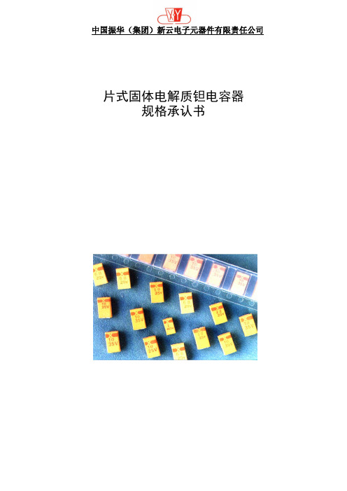
片式固体电解质钽电容器规格承认书1. 产品特点该产品为模压封装、片式引出,具有密封性好、重量轻、电性能优良、稳定可靠等特点。
适用于移动通讯、摄像机、程控交换机、计算机、汽车电子等各种电子设备的表面贴装直流或脉动电路。
2. 产品型号及编码说明CA45A - A - 16(15)V - 4.7μF - K型号 壳号 额定电压 标称电容量 容量偏差3. 产品外形及尺寸:见图1及表1表1 电容器的外形尺寸单位:mm4.电性能参数4.1 工作温度范围:-55℃~125℃;85℃以上施加降额电压。
4.2 标称电容量允许偏差(25℃,100Hz):K:±10%4.3 主要电性能参数:见表2表2 电性能参数表5.标志5.1标志内容(1)商标及正极标识(2)标称电容量(3)额定工作电压5.2 标志说明:见图2(举例)。
6. 产品外观质量6.1 产品本体应无针眼、缺角、缺块、发黑、漏封、裂纹、引出片断裂等现象。
6.2 产品标志:应清晰、完整、正确;无重影、漏打等现象。
7.包装7.1 产品编带的尺寸及卷绕方向:见图3、图4、表4、表5。
注:用户未要求时,编带卷绕方向通常按左旋卷绕方向。
7.2包装数量:见表3表3 包装数量7.3产品内外包装盒应无破损,料盘、小盒及外包装箱上应有相应物料标识单,标识应清楚、准确。
7.4每批产品应附产品合格证,内容包括产品型号、规格、壳号、容量级别、数量、生产批号及执图4表 4 编带尺寸单位:mm表 5 卷盘尺寸和数量8.典型试验要求:见表6表6 典型试验要求9 应用指南9.1室温电性能的测量9.1.1 电容量(C)和损耗角正切(tg δ)的测量●施加电压: 直流偏压:U-=2.20 -1.0V ;交流偏压(有效值)的范围:U ~=1.00-0.5V●测量时,确保电容器正、负极的接法正确,否则读数会产生较大的偏差。
9.1.2漏电流(I )的测量●施加电压:额定电压测量时,应串联1000Ω的保护电阻。
- 1、下载文档前请自行甄别文档内容的完整性,平台不提供额外的编辑、内容补充、找答案等附加服务。
- 2、"仅部分预览"的文档,不可在线预览部分如存在完整性等问题,可反馈申请退款(可完整预览的文档不适用该条件!)。
- 3、如文档侵犯您的权益,请联系客服反馈,我们会尽快为您处理(人工客服工作时间:9:00-18:30)。
承認書APPROVAL SHEET零件名稱:積層陶瓷電容Description :Multi-Layer Chip CapacitorDATE :20020099/1201深圳市宸远科电子有限公司ChipCera Technology CO.,LTD 深圳市宝安区银田工业区A9栋厂房TEL :+86-7+86-7555555--29120592FAX :+86-7+86-7555555--29120593Reference No.:PD0PD091201912019120100000011Customer Customer::宸遠科技料號CCT Part Numbers客戶料號Customer Customer’’s Part Numbers 宸遠科技ChipCera Technology Co.,LTD 客戶承認Customer Customer’’s Approval 製表Prepared by 審查Checked by 核准Approved byEngineer QA Manager Vice G.M.Tolerance Capacitance for dielectricA=±0.05pF B=±0.10pF C=±0.25pF D=±0.50pF F=±1.0% G=±2.0% J=±5.0% K=±10% M=±20%NP0X7R X5R Y5V 10pF and below More than10pF100pF~1μF(101~105)1uf~100uf(105~107)10nF~10uF(103~106) B,C,D G,J J,K,M K,M M,ZProduct dimensions in mm.X7R SeriesX7R/X5R SeriesY5V Series7Resistance tosoldering heatPreheat the capacitor at120℃to150℃for1minute.Immerse the capacitor in an eutectic soldersolution at270270±±5℃for1010±±1seconds.After set it atroom temperature for2424±±2hours(temperaturecompensation type)or4848±±4hours(high dielectricconstant type),then measure.*High dielectric constant type:Initial measurement of X7RX7R/X5R/X5R and Y5V.Perform a heat treatment at150150±±5℃for one hourand then set it at room temperature for4848±±4hours.Perform the initial measurement.Dielectric NP0X7RX7R//X5RY5VAppearance No defectCapacitanceChange<±2.5%or<±0.25pF±7.5%±20%DF The same as No.2IRMore than500500ΩΩ-F(whichever is smaller)DielectricStrengthNo failure8Resistance toleachingThe capacitors are dipped into the solder at260260±±5℃for3030±±1seconds,and then check the solderingby measuring the areas covered with solder.95%of the terminations are to be soldered evenly andcontinuously.9Solder ability ofterminationZero hour test,and test after storage(20to24months)in original atmosphere in normalatmosphere;un-mounted chips completelyimmersed for2±0.5s in a solder bath of235±5℃.95%of the termination is to be soldered evenly andcontinuously.10Rapid change oftemperatureNPO/X7R:-55℃to+125℃,5cycleX5R:-55℃to+85℃,5cycleY5V:-25℃to+85℃,5cycleDuration:30mins.Recovery:24±2hrs.No visible damage after24h recoveryClass I NPO:∆C/C≤2.5%or±0.25pFClassⅡX7RX7R/X5R/X5R/X5R::∆C/C≤±15%Y5V:∆C/C≤±20%11Damp heat,steadystate500±12hours at40±2℃;90to95%RHNo visible damage after24±2(NPO)or48±4hoursrecoveryClassⅠ(NPO)1.∆C/C±5%or1pF,whichever is greater2.C<10pF;Q≥200+10C10≤C≤30pF;Q≥275+5/2CC>30pF;Q≥3503.IR≥4000MΩorRiCR≥4040ΩΩF,whichever is lessClassⅡ(X7R(X7R/X5R/X5R/X5R))1.∆C/C within±15%2.2.tantanδ≤7%3.3.R R≥2000MΩorRiCR≥5050ΩΩF,whichever is lessClassⅡ(Y5V)1.∆C/C within±30%2.50/25V:tanδ≤9%16V:tanδ≤12.5%10V:tanδ≤15%3.IR≥2000MΩorRiCR≥5050ΩΩF,whichever is less12Endurance 1000h at maximum temperatureVr(rated voltage)≤250VAt2×V rVr(rated voltage)=500VAt1.5VrVr(rated voltage)>500VAt1.2VrC>0..1UF,At1.5VrNo visible damage after24±2(NPO)or48±4hoursrecoveryClass1(NPO)1.∆C/C±2%or1pF,whichever is greater2.tanδ≤2x specified value3.IR≥4000MΩor RiCR≥4040ΩΩF,whichever is lessClass2(X7R(X7R/X5R/X5R/X5R))1.∆C/C within±15%2.tanδ≤7%3.IR≥2000MΩor RiCR≥5050ΩΩF,whichever is lessClass2(Y5V)1.∆C/C within±30%2.50/25V:tanδ≤9%16V:tanδ≤12.5%3.IR≥2000MΩor RiCR≥5050ΩΩF,whichever is lessAll dimensions in mmSize SymbolABPLT(Paper)T(Embossed)04020.62±0.05 1.12±0.05 2.00±0.058.00±0.200.60±0.05N/A 0603 1.10±0.10 1.90±0.10 4.00±0.108.00±0.20 1.00±0.05N/A 0805 1.65±0.05 2.40±0.05 4.00±0.108.00±0.20 1.00±0.05N/A 1206 2.00±0.10 3.50±0.10 4.00±0.108.00±0.20 1.00±0.05Max.2.01210 2.80±0.20 3.70±0.20 4.00±0.108.00±0.20N/A Max.2.01808 2.50±0.30 4.90±0.30 4.00±0.1012.0±0.20N/A Max.2.518123.60±0.304.90±0.308.00±0.1012.0±0.20N/AMax.2.5Paper Tape T ≦1.1mmEmbossed Tape T ≦2.60mm8.4+1.5/-0 All dimensions in mm6.1Capacitor ClassificationMulti-layer ceramic capacitors are available in wide range of characteristics.Electronic Industries Association (EIA)and the military have established categories to help divide the basic characteristics into more easily specified classes.The basic indu industrystry specification for ceramic capacitor is EIA specification RS-198and as noted in the general section,it specifies temperature-compensating capacitors as class I capacitors.These are specified by the military under specification MIL-C-20.General-pur General-purposepose capacitors with non-linear temperature coefficients are called Class II capacitors by EIA and specified by military under MIL-C-11015and MIL-C-39014.The new high reliability military specification,MIL-C-123covers both class Iand class II dielect dielectrics.rics.Class I —Class I capacitors or temperature-compensating capacitors are usually made from mixtures of titanates where barium titanate is normally not a major part of mix.They have predictable temperature coefficients and in general,do not have an aging characteristic.Thus they are the most stable capacitor available.Normally the T.C.s of Class I temperature-compensating capacitors are NP0(±30ppm/℃).Class II —General-purpose ceramic capacitors are called Class II capacitors and have become extremely popular because of the high capacitance values available in very small size.These capacitors are ferroelectrics and vary in capacitance value under the influence of the environmental and electrical operating conditions.Class II capacitors are affected by temperature 、voltage 、frequency and time.Temperature effects for Class II ceramic capacitors are exhibited as non-linear capacitancechanges with tem temperature.perature.Industry standards for Mid-K dielectrics,such as X7R X7R/X5R /X5R and High-K dielectrics,such as Z5U Z5U..6.2The Characterization of MaterialsThe T.C curve of each material (for reference)DesignationClass Temperature Range (℃)Temp.Characteristics NPO(COG)I -55~+125±30ppm/℃X7RII -55~+125±15%X5RII -55~+85±15%Y5V II -25~+85-82~+22%6.3Recommend IR reflow and wave solderng profile(Pb-Free)Typical profile band of IR reflow Typical profile band of wave soldering。