PCI8360V PCI总线数据采集卡简明手册
National Instruments VXI-8360T产品数据手册说明书
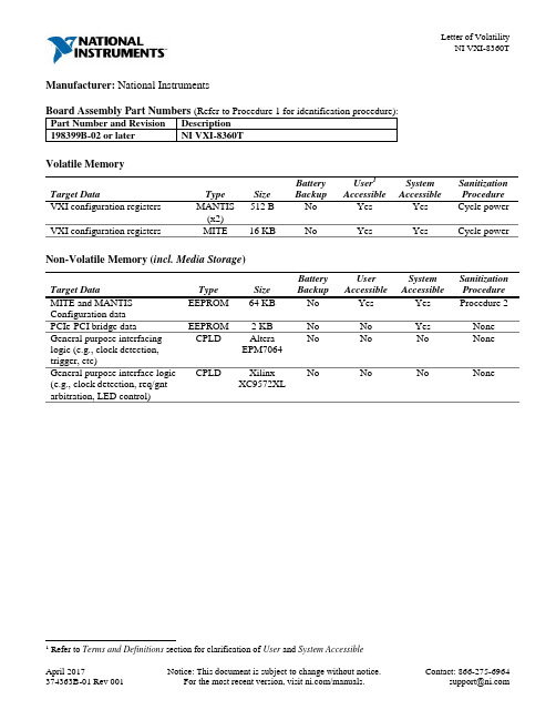
Manufacturer: National InstrumentsVolatile MemoryTarget Data Type Size BatteryBackupUser1AccessibleSystemAccessibleSanitizationProcedureVXI configuration registers MANTIS(x2)512 B No Yes Yes Cycle power VXI configuration registers MITE 16 KB No Yes Yes Cycle power Non-Volatile Memory (incl. Media Storage)Target Data Type Size Backup Accessible Accessible Procedure MITE and MANTISConfiguration dataEEPROM 64 KB No Yes Yes Procedure 2 PCIe-PCI bridge data EEPROM 2 KB No No Yes NoneGeneral purpose interfacing logic (e.g., clock detection, trigger, etc) CPLD AlteraEPM7064No No No NoneGeneral purpose interface logic (e.g., clock detection, req/gnt arbitration, LED control) CPLD XilinxXC9572XLNo No No None1 Refer to Terms and Definitions section for clarification of User and System AccessibleProceduresProcedure 1 – Board Assembly Part Number identification:To determine the Board Assembly Part Number and Revision, refer to the large label applied to the back surface of your product (on the non-removable aluminum module assembly cover). The Assembly Part Number should be formatted as “######a-##L”.Procedure 2 – MITE and MANTIS Data EEPROM:To clear the user-accessible data from the MITE and MANTIS Data EEPROM, complete the following steps:1.With jumper W5 in the default location (Boot from User Configuration), power on the computer. Thecomputer should boot this time because the factory-default configuration is being used to initialize theNI VXI-8360T controller.2.Right-click on the VXI system in MAX and select the Hardware Configuration utility.3.In the General tab under Quick Configuration select Default Configuration.4.Click Yes in the pop up box if you are sure you want to restore the factory defaults.5.Click OK in the hardware configuration panel to save the settings.6.After saving the configuration, restart the system for changes to take effect.Terms and DefinitionsCycle Power:The process of completely removing power from the device and its components and allowing for adequate discharge. This process includes a complete shutdown of the PC and/or chassis containing the device; a reboot is not sufficient for the completion of this process.Volatile Memory:Requires power to maintain the stored information. When power is removed from this memory, its contents are lost. This type of memory typically contains application specific data such as capture waveforms.Non-Volatile Memory:Power is not required to maintain the stored information. Device retains its contents when power is removed.This type of memory typically contains information necessary to boot, configure, or calibrate the product or may include device power up states.User Accessible:The component is read and/or write addressable such that a user can store arbitrary information to the component from the host using a publicly distributed NI tool, such as a Driver API, the System Configuration API, or MAX. System Accessible:The component is read and/or write addressable from the host without the need to physically alter the product. Clearing:Per NIST Special Publication 800-88 Revision 1, “clearing” is a logical technique to sanitize data in all User Accessible storage locations for protection against simple non-invasive data recovery techniques using the same interface available to the user; typically applied through the standard read and write commands to the storage device.Sanitization:Per NIST Special Publication 800-88 Revision 1, “sanitization” is a process to render access to “Target Data” on the media infeasible for a given level of effort. In this document, clearing is the degree of sanitization described.。
PCI-DAS6402-16数据采集接口卡说明书
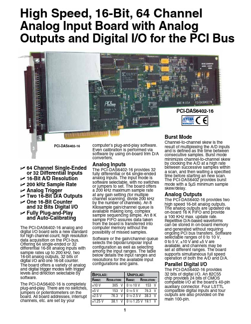
U64 Channel Single-Ended or 32 Differential InputsU16-Bit A/D ResolutionU200 kHz Sample RateU A nalog TriggerU T wo 16-Bit D/A Outputs U O ne 16-Bit Counterand 32 Bits Digital I/OU F ully Plug-and-Playand Auto-CalibratingThe PCI-DAS6402-16 analog and digital I/O board sets a new standard for high channel count, high resolution data acquisition on the PCI-bus. Offering 64 single-ended or 32 differential 16-bit analog inputs with sample rates up to 200 kHz, two16-bit analog outputs, 32 bits of digital I/O and one 16-bit counter. The board offers a variety of analog and digital trigger modes with trigger levels and direction selectable by software.The PCI-DAS6402-16 is completely plug-and-play. There are no switches, jumpers or potentiometers on the board. All board addresses, interrupt channels, etc. are set by your computer’s plug-and-play software. Even calibration is performed via software by using on-board trim D/A converters.Analog InputsThe PCI-DAS6402-16 provides 32 fully differential or 64 single-ended analog inputs. The input mode is software selectable, with no switches or jumpers to set. The board offers a 200 kHz maximum sample rateat any gain setting (for multiple channel scanning, divide 200 kHz by the number of channels). An 8 Kilosample gain/channel queue is available making long, complex sample sequencing simple. An 8 K sample FIFO assures data taken from the board is transferred into computer memory without the possibility of missed samples. Software or the gain/channel queue selects the bipolar/unipolar input configuration as well as selecting among the input ranges. The table below details the input ranges and resolutions for the available input configurations and gains.High Speed, 16-Bit, 64 Channel Analog Input Board with Analog Outputs and Digital I/O for the PCI BusPCI-DAS6402-16Burst ModeChannel-to-channel skew is the result of multiplexing the A/D inputs and is defined as the time between consecutive samples. Burst mode minimizes channel-to-channel skew by clocking the A/D at a high rate between successive samples within a scan, and then waiting a specified time before starting an new scan. The PCI-DAS6402 provides burst mode with a 5µS minimum sample skew/delay.Analog OutputsThe PCI-DAS6402-16 provides two high speed 16-bit analog outputs. The analog outputs are updated via on-board 16 K FIFO and providea 100 KHz max. update rate. Repetitive D/A-based waveforms can be stored in on-board memory and generated without requiring ongoing PCI bus transfers. Software selectable ranges of 0 to 10 V,0 to 5 V, ±10 V and ±5 V are available, and channels may beset at different ranges. The board supports simultaneous full speed operation of both the A/D and D/A. Parallel Digital I/OThe PCI-DAS6402-16 provides32 bits of digital I/O. An 82C55chip provides 24 bits of CMOS compatible I/O at the board’s 40-pin auxiliary connector. Four LSTTL compatible digital inputs and four outputs are also provided on the main 100-pin.PCI-DAS6402-16connector and installs in any unused slot. This 37-pin connector is then pin compatible with all DIO24 series boards (and all of our 8- and 24-bit digital signal conditioning boards). Alternatively, the 40-pin header may be brought out directly withthe C40FF-2 cable and connected directly to a CIO-MINI40 screw terminal board.Software SupportThe PCI-DAS6402 series is supplied with InstaCal software for calibration and test. In addition, it is also supported by the optional Universal Library. The Universal Library isa set of I/O libraries and driversfor those users creating their own custom programs. The Universal Library is compatible with most Windows (32-bit) based languages and supports the entire PCI-DAS and CIO families of boards. An optional driver for LabVIEW is also available. SpecificationsANALOG INPUTResolution: 16-bitsNumber of Channels: 32 diff/64 SE, software selectableA/D Conversion Time: 5 µs Sample Rate: 200 Khz (divide by number of channels in use) Programmable Ranges: ±10 V,±5 V, ±2.5 V, ±1.25 V, 0 to 10 V,0 to 5 V, 0 to 2.5 V, 0 to 1.25 VA/D Pacing: programmable: internal counter, external source or software polledChannel/Gain Queue: 8192 samples.Burst Mode: software selectable option, skew = 5 µsANALOGCounter/TimersThe PCI-DAS6402-16 provides one 16-bit down counter (1⁄3 of an 82C54). The counter provides clock, gate and output connections at the user I/O connector.WiringAll analog, triggering and counter/ timer connections are through a 100-pin high-density connector. The C100FF-XX series cable splits the 100 pins into separate 50-pin cables. The first 50-pin cable contains the signals from pins 1-50, while the second carries pins 51-100. These 50-pin connectors are compatible with the CIO-MINI50, and BNC-series of interconnects. The 24-bits of high current digital I/O are available on an 40 pin header. From the 40-pin header the user connect to the optional BP40-37 which brings these pins out to the standardA/D Trigger Sources:External: analog or digitalA/D TRIGGERING MODES Digital: SW configurable for edge (triggered) or level-activated (gated). programmable polarity (rising/falling edge, high/low gate).Analog: SW configurable for above/ below reference, in/out window and hysteresis.Pre-Trigger: unlimited pre- and post-trigger sample sizes, compatible with digital and analog trigger modes Diff. Linearity Error: ±1.25 V range, ±3 LSB, all other ranges ±1 LSBIntegral Linearity Error: ±1.25 V range, ±3 LSB. all other ranges,±1.5 LSBInput Leakage Current: 200 nA (25 Deg C)Input Impedance: 10 Meg Ohms, min Maximum Input Voltage: ±15 V COUNTERSConfiguration: one 16-bit down counter (1/3 of an 82C54)Clock Input Frequency: 10 Mhz max High Pulse Width (clk input): 30 ns minLow pulse Width (clk input):50 ns minGate Width High or Low: 50 ns min Input Low Voltage: 0.8 V max Input High Voltage: 2.0 V minOutput Low Voltage: 0.4 V maxOutput High Voltage: 3.0 V minANALOG OUTPUTSResolution: 16-bitsNumber of Channels: 2Voltage Ranges: ±10 V, ±5 V,0 to 5 V, 0 to 10 V. (each channelindependently programmable)D/A Update Rate: 100 KHz on eachD/A operating in single channel orsimultaneous update modeArbitrary Waveform Mode:supports repetitive waveforms to16 KsampleD/A Pacing: internal or externalclock or software pacedD/A Trigger Modes: software orexternal gateOffset Error: ±100 uV max, all rangesDifferential Nonlinearity:±1 LSB maxIntegral Nonlinearity: ±1 LSB maxSettling Time (10V step to.0008%): 6µs typSlew Rate: 10 V ranges, 6 V/uS.5 V ranges, 3 V/uSCurrent Drive: ±5 mA minShort-Circuit Current: ± 35 mAindefiniteOutput Impedance: 0.1 Ohms maxMiscellaneous: power up/reset, allDAC’s set to 0 voltsLLGND1IN0HI2IN32/IN0LO34567891011121314151617LLGND18IN8HI19202122232425262728293031323334DAORTN35VDAC036DA1RTN37VDAC138CTRCLK39CTRGATE40CTROUT_BUF41EXTADCCONVERT42ATRIGIN43DIN044TRIG145DIN146TRIG247VDD48STARTSCAN_BUF49GND50IN1HIIN33/IN1LOIN2HIIN34/IN2LOIN3HIIN35/IN3LOIN4HIIN36/IN4LOIN5HIIN37/IN5LOIN6HIIN38/IN6LOIN7HIIN39/IN7LOIN40/IN8LOIN9HIIN41/IN9LOIN10HIIN42/IN10LOIN11HIIN43/IN11LOIN12HIIN44/IN12LOIN13HIIN45/IN13LOIN14HIIN46/IN14LOIN15HIIN47/IN15LO51525354555657585960616263646566676869707172737475767778798081828384858687888990+12V91GND92-12V939495SCANCLK_BUF96979899XINT100GNDLLGNDIN16HIIN48/IN16LOIN17HIIN49/IN17LOIN18HIIN50/IN18LOIN19HIIN51/IN19LOIN20HIIN52/IN20LOIN21HIIN53/IN21LOIN22HIIN54/IN22LOIN23HIIN55/IN23LOLLGNDIN24HIIN56/IN24LOIN25HIIN57/IN25LOIN26HIIN58/IN26LOIN27HIIN59/IN27LOIN28HIIN60/IN28LOIN29HIIN61/IN29LOIN30HIIN62/IN30LOIN31HIIN63/IN31LODOUT0DOUT1DOUT2DOUT3GNDDIN2DIN3EXTDACUPDATEDACTRIGAIGATEPCI-DAS6402/16Main ConnectorPCI-DAS6402-16 100 Pin ConnectorNC1NC3PB75PB67PB59PB411PB313PB215PB117PB019GND21NC23GND25NC27GND29NC31GND33+5V35GND37NC392+5V4GND6PC78PC610PC512PC414PC316PC218PC120PC022PA724PA626PA528PA430PA332PA234PA136PA038NC40NCAuxiliary/Digital Connector DiagramPCI-DAS6402-16 40 Pin ConnectorDIGITAL I/O Digital Bits: 32Configuration: 24-bit, 82C55 at Aux 40-pin connector, 4 dedicated input & 4 dedicated output bits on 100-pin main connectorConfiguration: 2 banks of 8, 2 banks of 4, programmable by bank as input or outputDefault/Reset State: input, high impedance 82C55Output High: 2.4 volts @ -2.5 mA minOutput Low: 0.5 volts @ 2.5 mA minInput High: 2.0 volts min, 7 volts absolute maxInput Low: 0.8 volts max, -0.5 volts absolute minDEDICATED I/O BITS (4 input, 4 output)Input / Output Device: 74LS175Default/Reset State: all 4 outputs to logic lowOutput High: 2.4 volts @ -0.4 mA minOutput Low: 0.5 volts @ 8.0 mA minInput High: 2.0 volts min, 7 volts absolute maxInput Low: 0.8 volts max, -0.5 volts absolute minINTERRUPTSInterrupt Enable: software programmableInterrupt Sources: external(rising TTL edge event) or a variety of internal FIFO status sources ENVIRONMENTALOperating Temperature Range: 0 to 70°CStorage Temperature Range: -40 to 100°CHumidity: 0 to 90% non-condensingPower Consumption: operating, +**************,3.1AmaxOrdering Example:PCI-DAS6402-16 card, two CIO-MINI50 terminal panels, one C100FF-2 cable, one CIO-MINI40 terminal panel, one C40FF-2 cable, and OMEGACARE SM 1-year extended warranty for PCI-DAS6402-16(adds 1 year to standard 3-year warranty).The CIO-MINI50 screw terminal boardDASWizard is an optional software program that provides direct data collection into Microsoft Excel.OMEGACARE SM extendedwarranty program is available for models shown on this page. Ask your sales representative for full details when placing an order. OMEGACARE SM covers parts, labor and equivalent loaners.。
PC-836 快速说明书
PCL-836快速安装使用手册PCL-836快速安装使用手册 (1)第一章产品介绍 (1)1.1 概述 (1)1.1.1 独特的数字滤波器 (2)1.2 特点 (2)1.3 一般特性 (2)第二章 安装与测试 (2)2.1 初始检查 (2)2.2 开关和跳线的设置 (3)2.2.1 基址的选择 (3)2.2.2 中断优先级设置 (3)2.3 引脚图 (3)2.4 Windows2K/XP/9X下板卡的安装 (5)2.4.1 软件的安装: (5)2.4.2硬件的安装: (7)2.5 测试 (13)2.5.1 数字量输入功能测试 (14)2.5.2 数字量输出功能测试 (14)2.5.3 计数器功能测试 (15)第三章 信号的连接 (16)3.1 数字信号的连接 (16)第四章 例程使用详解 (17)4.1 板卡支持例程..........................................................................错误!未定义书签。
4.2 常用例子使用说明..................................................................错误!未定义书签。
4.2.1 DIGOUT(数字量输出): (17)4.2.2 COUNTER(计数程序) (19)4.2.3 Digin (数字量输入例程) (20)4.2.4 PULSE(脉冲输出例程) (20)第五章 遇到问题,如何解决? (21)第一章 产品介绍1.1 概述PCL-836是一款ISA插槽的计数器/定时器和数字量I/O卡。
该卡提供了6个16位计数器通道。
它还带有16路数字量输出和16路数字量输入。
卡上的2个8245芯片提供了各种计数器/定时器功能模式,是工业应用和实验室应用的理想选择。
1.1.1 独特的数字滤波器PCL-836带有1个独特的数字滤波器,可以消除输入信号中的噪声。
PCI数据卡采集与USB采集设备的使用

PCI数据卡采集与USB采集设备的使用一实验目的学习使用LabVIEW配置PCI接口内置式数据采集卡进行数据采集的方法;熟悉外置式便携测试仪器的概念,了解其产品特点与使用场合,学习使用USB接口的数据采集装置进行数据采集和信号发生。
二实验设备1、安装有LabVIEW 8.6计算机2、安装有NI-DAQ 8.6的计算机3、系统支持的PCI数据采集设备(DAQ)(NI公司的NI-PCI6014数据采集卡)。
4、安装有100MHz Handyscope HS3型多功能测试仪的PC5、HP惠普示波器探针工具包,空闲USB2.0接口6、荷兰TiePie Engineering公司USB接口高速多功能测试仪一台,参数如下,输入:2通道,分辨率12~16位,最高采样率100MHz,最大测试电压200V。
输出:14位精度,50MSamples/s,0~±12V。
三实验原理一个DAQ系统通常包括:数据采集DAQ设备,传感器,转换器,信号调节以及一套用于获得、处理数据和分析、显示、存储数据的软件。
基于计算机的测量系统,一般需要先通过传感器(或变送器)将物理信号转换成电信号(如电压或电流)。
在大多数情况下,在信号输入DAQ之前,还必须使用信号调理设备对所测量的信号进行放大和滤波,以提高信号增益和消除噪声干扰。
一般而言,所有能够在计算机控制下完成数据采集和控制任务的板卡产品都称为DAQ产品。
它们可以被分为内插式(plug-in)板卡和外挂式两大类。
内插式DAQ板卡包括基于ISA,PCI,PXI/Compact PCI,PCMCIA等总线的板卡,速度快,性能参数较高,适合大型的测试和控制场合,但不适合现场测试场合;外挂式DAQ板卡包括USB,PCMCIA,IEEE1394,RS232/RS485和并口板卡,用户可以将其带入工作测试现场,进行远程数据采集和控制应用,使用方便,但性能参数相对较低。
◎插入式DAQ卡采集卡直接接入计算机,接口为PCI、ISA等。
05 监控篇之PCI数据采集卡

3.数字量输入/输出卡(I/O卡)
计算机测控系统通过数字量输入板卡采 集工业生产过程的离散输入信号,并通过数 字量输出板卡对生产过程或控制设备进行开 关式控制(二位式控制)。
将数字量输入和数字量输出功能集成在 一块板卡上,就称为数字量输入/输出板卡, 简称I/O板卡。
例如,下图所示为研华PCI-1730数字量输入/输出卡, 它提供了16路数字量输入和16路数字量输出,高输出驱动能 力和中断能力,具有2500VDC高电压隔离I/O通道。
数据采集系统概述
数据采集系统的任务,就是传感器从被测对 象获取有用信息,并将其输出信号转换为计算机 能识别的数字信号,然后送入计算机进行相应的 处理,得出所需的数据。同时,将计算得到的数 据进行显示、储存或打印,以便实现对某些物理 量的监视,其中一部分数据还将被生产过程中的 计算机控制系统用来进行某些物理量的控制。
数据采集系统性能的好坏,主要取决于它的 精度和速度。在保证精度的条件下,应有尽可能 高的采样速度,以满足实时采集、实时处理和实 时控制对速度的要求。
数据采集系统概述
2、 现代数据采集系统的特点:
1)现代数据采集系统一般都内含有计算机系统, 这使得数据采集的质量和效率等大为提高,同时 显著节省了硬件投资。 2)软件在数据采集系统中的作用越来越大,增加 了系统设计的灵活性。 3)数据采集与数据处理相互结合得日益紧密,形 成了数据采集与处理相互融合的系统,可实现从 数据采集、处理到控制的全部工作。
数据采集卡的性能优劣对整个系统举足轻重。选购时 不仅要考虑其价格,更要综合考虑,比较其质量、软件支持 能力、后续开发和服务能力等。
基于数据采集卡的控制系统组成
基于板卡的计算机测控系统的组成如图所示,它可分 为硬件和软件两大部分。
红日 PCI 光栅和编码器数据采集卡 说明书

PCI光栅和编码器数据采集器RSPCIRS说明书西安红日科技Tel************Fax************ Web:QQ:282429943目录第一章功能描述 (3)第二章外观 (4)第三章引脚说明 (5)第四章工作环境 (6)第五章驱动软件安装 (7)第六章DEMO应用程序安装 (8)第七章二次开发动态连接库涵数接口说明 (9)第一章功能描述1、过零位清零功能、过零位次数输出(圈数1M的计数长度±524287;脉冲计数4M的计数长度±2097151)。
2、每轴输入两路90度相位差信号。
采集器完成4细分。
3、圈数与脉冲计数辩向功能。
4、计数值圈数1M的计数长度±524287;脉冲计数4M的计数长度±2097151。
5、过零位清零功能可程控。
6、最高允许300MHz的信号输入。
7、可接入四个编码器或16个光栅信号输入。
8、PCI自供电,不需电源。
9、输入高电平最低电位1.51V,输入高电平最高电位5V。
10、输入低电平最高电位1.49V,输入低电平最低电位-0.5V。
11、过零中断功能可程控,中断后上报过零后的圈数和脉冲计数。
第二章外观.第三章引脚说明编码器或光栅信号输入(34芯)PIN号名称说明1AIN+A第一路编码器+A输入14AIN+B第一路编码器+B输入2AIN+Z第一路编码器过零+Z输入15AIN-A第一路编码器-A输入3AIN-B第一路编码器-B输入16AIN-Z第一路编码器过零-Z输入4BIN+A第二路编码器+A输入17BIN+B第二路编码器+B输入5BIN+Z第二路编码器过零+Z输入18BIN-A第二路编码器-A输入6BIN-B第二路编码器-B输入19BIN-Z第二路编码器过零-Z输入7CIN+A第三路编码器+A输入20CIN+B第三路编码器+B输入8CIN+Z第三路编码器过零+Z输入21CIN-A第三路编码器-A输入9CIN-B第三路编码器-B输入22CIN-Z第三路编码器过零-Z输入10DIN+A第四路编码器+A输入23DIN+B第四路编码器+B输入11DIN+Z第四路编码器过零+Z输入24DIN-A第四路编码器-A输入12DIN-B第四路编码器-B输入25DIN-Z第四路编码器过零-Z输入13地线GND第四章工作环境工作温度:-40℃-+120℃存储温度:-50℃-+160℃第五章驱动软件安装1、把卡插入PC的PCI插槽2、运行光盘中的install.bat3、系统提示找到新的硬件,选择“从列表或指定位置安装(高级),再点击“下一步”用浏览器指到”光盘的/WDXPDRIVER“目录。
PCI8602硬件使用说明书
硬件使用说明书
北京阿尔泰科技发展有限公司产品研发部修订北京阿尔泰科技发展有限公司
目录
目 录 ...............................................................................................................................................................................1 第一章 功能概述 .....................................................................................................................................................3 第一节、产品应用 ...........................................................................................................................................3 第二节、AD 模拟量输入功能.........................................................................................................................3 第三节、DA 模拟量输出功能.................................................................................................
PCI-8340硬件说明书

PCI-8340 高速模入接口卡技术说明书1. 概述PCI-8340高速模入接口卡适用于提供了PCI 总线插槽的PC系列微机,具有即插即用(PnP)的功能。
其操作系统可选用目前流行的 Windows 系列、高稳定性的Unix等多种操作系统以及专业数据采集分析系统LabVIEW 等软件环境。
在硬件的安装上也非常简单,使用时只需将接口卡插入机内任何一个PCI总线插槽中并用螺丝固定,信号电缆从机箱外部直接接入。
PCI-8340高速模入接口卡安装使用简便、功能齐全。
其A/D 转换启动方式可以选用程控频率触发、程控单步触发、外部TTL信号触发以及外部时钟同步触发等多种方式。
A/D转换后的数据结果通过先进先出存储器(FIFO)缓存后由PCI总线读出。
为方便用户,本卡还提供了TTL电平的16路数字量输入和16路数字量输出信号通道,这些信号通道由卡后端40芯扁平电缆转换为37芯D型插头提供给用户。
2. 主要技术参数2.1模入部分( 标*为出厂标准状态,下同 )2.1.1输入通道数:单端16路 *;双端8路2.1.2 输入信号范围:0~10V*,±5V,0~5V2.1.3 输入阻抗:≥10MΩ2.1.4 输入通道选择方式:单通道程序指定/多通道自动扫描2.1.5 A/D转换分辩率:12位2.1.6 A/D采样程控频率:1KHz/5KHz/10KHz/50KHz/100KHz/200KHz2.1.7 A/D启动方式:程控频率触发/程控单步触发/外部TTL信号触发/外部时钟同步触发2.1.8 A/D转换非线性误差:±1LSB2.1.9 A/D转换输出码制:单极性原码*/双极性偏移码2.1.10 FIFO存储器容量:8K×16bit(全满)/4K×16bit(半满)2.1.11 数据读取识别方式:FIFO半满查询/FIFO非空查询/FIFO半满中断2.1.12 系统综合误差:≤0.1%F.S2.2 开关量部分2.2.1 输入路数:16路TTL电平2.2.2 输出路数:16路TTL电平2.3 电源功耗: +5V(±10%)≤500mA2.4环境要求:工作温度:10℃~40℃相对湿度: 40%~80%存贮温度:-55℃~+85℃2.5 外型尺寸:( 不含档板 )长×高=175.0mm×106.7mm ( 6.89英寸×4.2英寸)3. 工作原理3.1 工作原理简介PCI-8340 高速模入接口卡主要由高速多路模拟开关选通电路、高速高精度放大电路、高速模数转换电路、先进先出(FIFO)缓冲存储器电路、开关量输入输出电路和接口控制逻辑电路等部分组成。
- 1、下载文档前请自行甄别文档内容的完整性,平台不提供额外的编辑、内容补充、找答案等附加服务。
- 2、"仅部分预览"的文档,不可在线预览部分如存在完整性等问题,可反馈申请退款(可完整预览的文档不适用该条件!)。
- 3、如文档侵犯您的权益,请联系客服反馈,我们会尽快为您处理(人工客服工作时间:9:00-18:30)。
PCI8360V简明手册
!警告:
×接触本采集卡前请确保释放掉身体上的静电,否则静电有可能造成板卡永久性的损坏。
特性
♦模入部分:
输入通道数:单端32路,双端16路
输入信号范围:0~10V,-5V~+5V
输入精度:12Bit
最大采样频率:75KHz
启动转换方式:软件启动
♦开关量部分:
电平方式:TTL
输入通道数:16路
输出通道数:16路
♦计数器部分:
使用芯片:82C54兼容器件
输入通道数:3路
输出通道数:3路
♦电源功耗:+5V@500mA
♦使用环境要求:
工作温度:0℃~50℃
相对湿度:40%~80%
存贮温度:-40℃~+120℃
外形尺寸:长×高=175.6mm X98.3mm
布局图(阴影部分是跳线出厂设置)
出厂设置
AD输入范围(JP1,JP3,JP4,JP5)单极性0~10V
AD输入方式(JP2,JP6)单端
计数器控制(JP8)三个计数器全部外接
J1(模拟量输入和计数器输出接口)D型头
插座引脚号信号定义插座引脚号信号定义
1AD0(AD0+)20AD16(AD0-)
2AD1(AD1+)21AD17(AD1-)
3AD2(AD2+)22AD18(AD2-)
4AD3(AD3+)23AD19(AD3-)
5AD4(AD4+)24AD20(AD4-)
6AD5(AD5+)25AD21(AD5-)
7AD6(AD6+)26AD22(AD6-)
8AD7(AD7+)27AD23(AD7-)
9AD8(AD8+)28AD24(AD8-)
10AD9(AD9+)29AD25(AD9-)
11AD10(AD10+)30AD26(AD10-)
12AD11(AD11+)31AD27(AD11-)
13AD12(AD12+)32AD28(AD12-)
14AD13(AD13+)33AD29(AD13-)
15AD14(AD14+)34AD30(AD14-)
16AD15(AD15+)35AD31(AD15-)
17AGND36DGND
18OUT237OUT1
19OUT0
注:ADx表示模拟量输入的第x通道,括号外的为单端定义,括号内的是双端定义AGND指模拟地,单端使用时为信号地
为防止引入现场干扰,不应该使信号引脚悬空,可以将不使用的信号引脚与模拟地短路
OUTx表示计数器输出的第x个通道
DGND为数字地,注意模拟地和数字地不要接到一起
J2(开关量输入输出和计数器输入接口40PIN)
插座引脚号信号定义插座引脚号信号定义
40PIN_1DI040PIN_2DI1
40PIN_3DI240PIN_4DI3
40PIN_5DI440PIN_6DI5
40PIN_7DI640PIN_8DI7
40PIN_9DI840PIN_10DI9
40PIN_11DI1040PIN_12DI11
40PIN_13DI1240PIN_14DI13
40PIN_15DI1440PIN_16DI15
40PIN_17DO040PIN_18DO1
40PIN_19DO240PIN_20DO3
40PIN_21DO440PIN_22DO5
40PIN_23DO640PIN_24DO7
40PIN_25DO840PIN_26DO9
40PIN_27DO1040PIN_28DO11
40PIN_29DO1240PIN_30DO13
40PIN_31DO1440PIN_32DO15
40PIN_33DGND40PIN_34DGND
40PIN_35CLK040PIN_36CLK1
40PIN_37CLK240PIN_38DGND
40PIN_39DGND40PIN_40DGND
注:DIx表示开关量输入的第x通道
DOx表示开关量输出的第x通道
CLKx表示计数器输入的第x通道
DGND指开关量信号地
为了用户接线方便,我们随卡提供一根转接线,把卡上的J2(40PIN)转换为DB37(37芯D型头),引到计算机机箱外部。
DB37的引脚与开关量等信号的对照关系见下表:
插座引脚号信号定义插座引脚号信号定义
DB37_1DI0DB37_20DI1
DB37_2DI2DB37_21DI3
DB37_3DI4DB37_22DI5
DB37_4DI6DB37_23DI7
DB37_5DI8DB37_24DI9
DB37_6DI10DB37_25DI11
DB37_7DI12DB37_26DI13
DB37_8DI14DB37_27DI15
DB37_9DO0DB37_28DO1
DB37_10DO2DB37_29DO3
DB37_11DO4DB37_30DO5
DB37_12DO6DB37_31DO7
DB37_13DO8DB37_32DO9
DB37_14DO10DB37_33DO11。