
PT4115规格书
深圳市鑫宝宏电子有限公司 电话:13670037219 QQ:1561451328 Page 3
电气参数(续)(注 4、5)
PT4115
30V/1.2A、高调光比 LED 恒流驱动器
符号
参数
测试条件 最小值 典型值
DIM输入
RDIM
DIM对内部工作电压上拉电阻
200
IDIM_L
DIM接地漏电流
110
24V 1LED
10524V 3LED10012V 1LED
95
12V 3LED
90 -55 -35 -15 5 25 45 65 85 105 125
Ambient Temperature Switch "on" Resistance vs Temp
1.0
Vin=12V
0.9
0.8
0.7
0.6
包装运输
Tape and Reel 1000 units
Tape and Reel 2500 units
产品打印
PT4115 xxxxxX
PT4115 xxxxxX
华润矽威科技(上海)有限公司 PT4115_DS Rev CH_2.7
深圳市鑫宝宏电子有限公司 电话:13670037219 QQ:1561451328 Page 1
DIM管脚在正常工作时可以浮空。当加在DIM上的电压低 于0.3V时,内部功率开关关断,LED电流也降为零。关断 期间,内部稳压电路保持待机工作,静态电流仅为95uA。
DIM 管脚也可以通过外加直流电压(VDIM) 调小 LED 电流 (模拟调光),最大 LED 电流由采样电阻 RS 决定。直流 电压(VDIM) 的有效的调光范围是 0.5V 到 2.5V。当直流电 压(VDIM)高于 2.5V,输出 LED 电流保持恒定,并由(0.1/RS) 设定。LED 电流还可以通过 DIM 到地之间接一个电阻到
压降决定,在RS上产生一个压差VCSN, 当(VIN-VCSN) > 115mV时,CS比较器的输出变低,内部功率开关关断, 电流以另一个斜率流过电感(L)、电流采样电阻(RS)、 LED和肖特基二极管(D),当(VIN-VCSN) < 85mV时,功
率开关重新打开,这样使得在LED上的平均电流为
I OUT
DIM浮空
fOSC=500kHz fDIM =100Hz fDIM =20KHz
最小值 6
典型值
5.1 500
最大值 30
1
单位 V V mV
MHz
95
98
101
mV
99
102
105
mV
±15
%
8
µA
95
µA
5 2.5
0.5
0.02%
V
V
0.3
V
2.5
V
50
kHz
1
5000:1
4%
1
25:1
华润矽威科技(上海)有限公司 PT4115_DS Rev CH_2.7
散热端,内部接地,贴在 PCB 板上减小热阻
无连接,接地或悬空
极限参数(注 1)
符号 VIN SW CSN DIM ISW PDMAX PTR PTR TJ TSTG
参数
电源电压 功率开关的漏端 电流采样端 (相对 VIN) 开关使能、模拟和 PWM 调光端 功率开关输出电流 功耗(注 2)
热阻, SOT89-5(θJA) 热阻, ESOP-8(θJA)
深圳市鑫宝宏电子有限公司 电话:13670037219 QQ:1561451328 Page 2
PT4115
推荐工作范围
30V/1.2A、高调光比 LED 恒流驱动器
符号 参数
参数范围
单位
VIN
电源电压
0 ~ 30
V
TOPT
工作温度
-40 to +85
oC
注 1:最大极限值是指超出该工作范围,芯片有可能损坏。推荐工作范围是指在该范围内,器件功能正常,但并不完全
应用
z 低压 LED 射灯代替卤素灯 z 车载 LED 灯 z LED 备用灯 z LED 信号灯
封装
温度范围
SOT89-5 -40 oC 到 85 oC
定购型号 PT4115-89E
ESOP8
-40 oC 到 85 oC
PT4115-SOH
Note:
xxxxxX
典型应用电路
Assembly Factory Code Lot Number
VDIM = 0
25
功率开关
RSW
SW导通电阻
VIN =24V VIN =12V
0.4 0.6
ISWmean
SW连续电流
ILEAK
SW漏电流
0.5
过热保护
TSD
过热保护温度
160
TSD-hys 过热保护迟滞
20
注 4:典型参数值为 25˚C 下测得的参数标准。
注 5:规格书的最小、最大规范范围由测试保证,典型值由设计、测试或统计分析保证。
Shutdown Current vs Supply Voltage
120
110
100
90
80
70
60
50
40
30
20
10
0
0
5
10 15 20 25 30
Iin(uA)
Iin (uA)
"on" Resostence(ohm)
Vsense (V)
Voltage across Rcs(0.33ohm) vs Temperature 115
测试条件
VIN下降 VIN 上升
平均采样电压
采样电压迟滞 CSN管脚输入电流
A档 VIN- VCSN B 档 VIN-VCSN=50mV
关断电流
VDIM<0.3V
内部电路工作电压 DIM输入高电平 DIM输入低电平 模拟调光电压范围 最大PWM调光频率 低 频 PWM 调 光 占 空 比 范围 低频PWM调光比 高 频 PWM 调 光 占 空 比 范围 低频PWM调光比
PT4115
30V/1.2A、高调光比 LED 恒流驱动器
管脚
管脚描述
管脚号 1 2 3 4 5
-
ESOP8 4,5
CSN VIN SW NC
1
8 DIM
PT4115
2
7 GNDA
3
6 GNDP
4
5
NC
ESOP8
管脚名称 SW GND DIM CSN VIN
Exposed PAD NC
描述
功率开关的漏端 信号和功率地 开关使能、模拟和 PWM 调光端 电流采样端,采样电阻接在CSN和VIN端之间 电源输入端,必须就近接旁路电容
6 5 4 3 2 1 0
0123456789
Vdim vs Supply Vin
Vdim(V)
Vdim vs Supply Voltage
5.5
5.4
5.3
5.2
5.1
5.0
4.9
4.8
4.7
4.6
4.5 5
10
15
20
25
30
Supply Voltage Vin(V)
Efficiency
Vdim(V)
保证满足个别性能指标。电气参数定义了器件在工作范围内并且在保证特定性能指标的测试条件下的直流和交流电参数
规范。对于未给定上下限值的参数,该规范不予保证其精度,但其典型值合理反映了器件性能。
注 2:温度升高最大功耗一定会减小,这也是由 TJMAX, θJA,和环境温度 TA 所决定的。最大允许功耗为 PDMAX = (TJMAX TA)/ θJA 或是极限范围给出的数字中比较低的那个值。 注 3:人体模型,100pF 电容通过 1.5kΩ 电阻放电。
电气参数(注 4, 5)
无特别说明 VIN=12V, TA=25 oC
符号 VIN VUVLO VUVLO, HYS FSW
电流采样
VCSN
VCSN_hys ICSN
关断电流
IOFF DIM输入
VDIM VDIM_H VDIM_L VDIM_DC
fDIM
DPWM_LF
DPWM_HF
参数
输入电压 欠压保护 欠压保护迟滞 最大工作频率
简化模块图
最大值
1.2 5
单位
KΩ uA
Ω A µA
℃ ℃
工作原理描述
PT4115和电感(L)、电流采样电阻(RS)形成一个自 振荡的连续电感电流模式的降压型恒流LED控制器。 VIN上电时,电感(L)和电流采样电阻(RS)的初始电 流为零,LED输出电流也为零。这时候,CS比较器的输出 为高,内部功率开关导通,SW的电位为低。电流通过电 感(L)、电流采样电阻(RS)、LED和内部功率开关 从VIN流到地,电流上升的斜率由VIN、电感(L)和LED
工作结温范围 储存温度范围 ESD (注 3)
参数范围 -0.3~45 -0.3~45
+0.3~(-6.0) -0.3~6 1.5 1.5 45 40
-40 to 150 -55 to 150
2
单位 V V V V A W
oC /W oC /W
oC oC kV
华润矽威科技(上海)有限公司 PT4115_DS Rev CH_2.7
定购信息
z 极少的外部元器件 z 很宽的输入电压范围:从 6V 到 30V z 最大输出 1.2A 的电流 z 复用 DIM 引脚进行 LED 开关、模拟调光和 PWM 调光 z 5%的输出电流精度 z LED 开路自然保护 z 高达 97%的效率 z 输出可调的恒流控制方法 z 增强散热能力的 ESOP8 封装可用于大功率驱动
PT4115E

LED Driver with 5000:1 DimmingGENERAL DESCRIPTIONThe PT4115 is a continuous conduction mode inductive step-down converter, designed for driving single or multiple series connected LED efficiently from a voltage source higher than the total LED chain voltage. The device operates from an input supply between 8V and 30V and provides an externally adjustable output current of up to 1.2A. Depending upon the supply voltage and external components, the PT4115can provide more than 30 watts of output power.The PT4115 includes the power switch and a high-side output current sensing circuit, which uses an external resistor to set the nominal average output current, and a dedicated DIM input accepts either a DC voltage or a wide range of pulsed dimming. Applying a voltage of 0.3V or lower to the DIM pin turns the output off and switches the device into a low current standby state.The PT4115 is available in SOT89-5 and ESOP8 packages.FEATURESz Simple low parts countz Wide input voltage range: 8V to 30V z Up to 1.2A output currentz Single pin on/off and brightness control using DC voltage or PWMz Up to 1MHz switching frequency z Typical 5% output current accuracy z Inherent open-circuit LED protection z High efficiency (up to 97%) z High-Side Current Sensez Hysteretic Control: No Compensatio z Adjustable Constant LED CurrentzESOP8 package for large output power applicationAPPLICATIONSz Low voltage halogen replacement LEDs z Automotive lightingz Low voltage industrial lighting z LED back-up lighting z Illuminated signs z SELV lightingzLCD TV backlightingORDERING INFORMATIONPACKAGETEMPERATURERANGE ORDERING PARTNUMBERTRANSPORT MEDIA MARKING SOT89-5 -40 o C to 85 o C PT4115-89ETape and Reel1000 units PT4115 xxxxxX ESOP8 -40 o C to 85 o C PT4115-SOHTape and Reel2500 unitsPT4115 xxxxxXNote:TYPICAL APPLICATION CIRCUITAssembly Factory CodeLot NumberLED Driver with 5000:1 DimmingPIN ASSIGNMENTPIN DESCRIPTIONSPIN No. PIN NAMES DESCRIPTION1 SW Switch Output. SW is the drain of the internal N-Ch MOSFET switch. 2GNDSignal and power ground. Connect directly to ground plane.3 DIMLogic level dimming input. Drive DIM low to turn off the current regulator.Drive DIM high to enable the current regulator. 4 CSN Current sense input5 VIN Input Supply Pin. Must be locally bypassed.- Exposed PADInternally connected to GND. Mount on board for lower thermal resistance. ESOP8 4,5NCNo connectionABSOLUTE MAXIMUM RATINGS (note1)SYMBOLITEMSV ALUE UNIT V IN Supply V oltage -0.3~45V SW Drain of the internal power switch -0.3~45 V CSN Current sense input (Respect to VIN) +0.3~(-6.0) V DIM Logic level dimming input -0.3~6VI SW Switch output current 1.5 A P DMAX Power Dissipation (Note 2)1.5 W P TR Thermal Resistance, SOT89-5 θJA 45 o C /W P TR Thermal Resistance, ESOP8 θJA 40 oC /WT J Operation Junction Temperature Range-40 to 150 o C T STG Storage Temperature-55 to 150oCESD Susceptibility (Note 3)2kVCSN VIN SW NCNCDIM ESOP830V , 1.2A Step-down High BrightnessLED Driver with 5000:1 DimmingPT4115RECOMMENDED OPERATING RANGESYMBOL ITEMSV ALUE UNIT V IN V DD Supply V oltage 0 ~ 30 VT OPTOperating Temperature-40 to +85oCNote 1: Absolute Maximum Ratings indicate limits beyond which damage to the device may occur. RecommendedOperating Range indicates conditions for which the device is functional, but do not guarantee specific performance limits. Electrical Characteristics state DC and AC electrical specifications under particular test conditions which guarantee specific performance limits. This assumes that the device is within the Operating Range. Specifications are not guaranteed for parameters where no limit is given, however, the typical value is a good indication of device performance.Note 2: The maximum power dissipation must be derated at elevated temperatures and is dictated by T JMAX , θJA , and the ambient temperature T A . The maximum allowable power dissipation is P DMAX = (T JMAX - T A )/ θJA or the number given in Absolute Maximum Ratings, whichever is lower.Note 3: Human body model, 100pF discharged through a 1.5k Ω resistor.ELECTRICAL CHARACTERISTICS (Note 4, 5)The following specifications apply for V IN =12V , T A =25 o C, unless specified otherwise. SYMBOL ITEMSCONDITIONS Min. Typ. Max. UNIT V IN Input Voltage 8 30 VV UVLO Under voltage lock out V IN falling 6.8 V V UVLO, HYS UVLO hysterisisV IN rising 500 mV F SW Max. Switching Frequency1MHzCurrent SenseA type 95 98 101 mV V CSNMean current sense threshold voltage V IN -V CSNB type99 102 105 mV V CSN_hys Sense threshold hysteresis±15%I CSNCSN Pin Input Current V IN -V CSN =50mV 8 µAOperating CurrentI OFF Quiescent supply current with output off V DIM <0.3V 95 µADIM InputV DIM Internal supply voltage DIM floating 5 V V DIM_H DIM input voltage High 2.5 V V DIM_L DIM input voltage Low 0.3VV DIM_DC DC brightness control0.52.5 Vf DIMMax. DIM Frequency f OSC =500kHz 50 kHz Duty cycle range of lowfrequency dimming f DIM =100Hz 0.02% 1 D PWM_LFBrightness control range5000:1LED Driver with 5000:1 DimmingELECTRICAL CHARACTERISTICS (Continued) (Note 4, 5)SYMBOL ITEMSCONDITIONSMin.Typ.Max.UNITDIM InputDuty cycle range of highfrequency dimming f DIM =20KHz4% 1 D PWM_HFBrightness control range25:1R DIM DIM pull up resistor to Internal supply voltage200 K Ω I DIM_L DIM input leakage lowV DIM = 025uAOutput SwitchVIN =12V 0.6 R SW SW On Resistance VIN=24V0.4 Ω I SWmeanContinuous SW Current1.2AI LEAK SW Leakage Current0.5 5 µA Thermal ShutdownT SD Thermal Shutdown Threshold 160 ℃ T SD -hys Thermal Shutdown hysteresis20 ℃Note 4: Typical parameters are measured at 25˚C and represent the parametric norm.Note 5: Datasheet min/max specification limits are guaranteed by design, test, or statistical analysis.SIMPLIFIED BLOCK DIAGRAMLED Driver with 5000:1 DimmingOPERATION DESCRIPTIONThe device, in conjunction with the coil (L1) and current sense resistor (RS), forms a self oscillating continuous-mode buck converter.When input voltage VIN is first applied, the initial current in L1 and RS is zero and there is no output from the current sense circuit. Under this condition, the output of CS comparator is high. This turns on an internal switch and switches the SW pin low, causing current to flow from VIN to ground, via RS, L1 and the LED(s). The current rises at a rate determined by VIN and L1 to produce a voltage ramp (V CSN ) across RS. When (V IN -V CSN ) > 115mV, the output of CS comparator switches low and the switch turns off. The current flowing on the RS decreases at another rate. When (V IN -V CSN ) < 85mV, the switch turns on againand the mean current on the LED is determined by851152()/100/S S mV R mV R +=.The high-side current-sensing scheme and on-board current-setting circuitry minimize the number of external components while delivering LED current with ±5% accuracy, using a 1% sense resistor.The PT4115 allow dimming with a PWM signal at the DIM input. A logic level below 0.3V at DIM forces PT4115 to turn off the LED and the logic level at DIM must be at least 2.5V to turn on the full LED current. The frequency of PWM dimming ranges from 100Hz to more than 20 kHz.The DIM pin can be driven by an external DC voltage(V DIM ) to adjust the output current to a value below the nominal average value defined by RS. The DC voltage is valid from 0.5V to 2.5V. When the dc voltage is higher than 2.5V, the output current keeps constant. The LED current also can be adjusted by a resistor connected to the DIM pin. An internal pull-up resistor (typical 200K Ω) is connected to a 5V internal regulator. The voltage of DIM pin is divided by the internal and external resistor.The DIM pin is pulled up to the internal regulator (5V) by a 200K Ω resistor. It can be floated at normal working. When a voltage applied to DIM falls below the threshold (0.3V nom.), the output switch is turned off. The internal regulator and voltage reference remain powered during shutdown to provide the reference for the shutdown circuit. Quiescent supply current during shutdown is nominally 95uA and switch leakage is below 5uA.Additionally, to ensure the reliability, the PT4115 is built with a thermal shutdown (TSD) protection and a thermal pad. The TSD protests the IC from over temperature (160℃). Also the thermal pad enhances power dissipation. As a result, the PT4115 can handle a large amount of current safely.LED Driver with 5000:1 DimmingTYPICAL PERFORMANCE CHARACTERISTICS8101214161820222426283075%80%85%90%95%100%E f f i c i e n c ySupply Voltage Vin(V)01234567890123456V d i m (V )Vdim vs Supply VinVdim vs Supply Voltage510152025304.54.64.74.84.95.05.15.25.35.45.5V d i m (V )Supply Voltage Vin(V)Vdim vs Supply Voltage-40-200204060801001205.005.055.105.155.205.255.30V d i m (V )Temperature(Deg C)Vdim vs Temperature9095100105110115V s e n s e (V )Ambient TemperatureVoltage across Rcs(0.33ohm) vs TemperatureLED Driver with 5000:1 Dimming51525350.30.40.50.60.70.80.91.0R s w (o h m )Supply Voltage Vin(V)Rsw vs Supply Voltage-500501001500.30.40.50.60.70.80.91.0"o n " R e s os t e n c e (o h m )Ambient Temperature Switch "on" Resistance vs Temp510152025300102030405060708090100110120S u p p l y V o l t a g e V i n (V )Iin(uA)Shutdown Current vs Supply Voltage0510********50100150200250I i n (u A )Supply Voltage Vin(V)Supply Current vs Supply Voltage0100200300400500600O u t p u t C u r r e n t (u A )Dim Duty Cycle100200300400500600700800L E D C u r r e n t (u A )Dim Pin Voltage(V)510152025300%10%20%30%40%50%60%70%80%90%100%D u t y C y c l eSupply Voltage Vin(V)Supply Voltage Vin(V)710720730740750760770780790800O u t p u t C u r r e n t (m A )Supply Voltage Vin(V)51015202530-6%-4%-2%0%2%4%6%O u t p u t C u r r e n t D e v i a t i o nSupply Voltage(V)Output Current L=47uH Rcs=0.13ohmLED Driver with 5000:1 DimmingD u t y C y c l eDuty Cycle L=47uH Rcs=0.13ohmSwitch Frequency L=47uH Rcs=0.13ohm51015202530280285290295300305310315320325O u t p u t C u r r e n tSupply Voltage (V)Supply Voltage0%10%20%30%40%50%60%70%80%90%D u t y C y c l eSupply Voltage Vin(V)Supply Voltage Vin(V)Switch Frequency L=100uH R=0.33ohmLED Driver with 5000:1 DimmingLED Driver with 5000:1 DimmingAPPLICATION NOTESSetting nominal average output current with external resistor RSThe nominal average output current in the LED(s) is determined by the value of the external current sense resistor (RS) connected between VIN and CSN and is given by:Rs I OUT /1.0= )082.0(Ω≥RsThis equation is valid when DIM pin is float or applied with a voltage higher than 2.5V (must be less than 5V). Actually, RS sets the maximum average current which can be adjusted to a less one by dimming.Output current adjustment by external DC control voltageThe DIM pin can be driven by an external dc voltage (VDIM), as shown, to adjust the output current to avalue below the nominal average value defined by RS.The average output current is given by:RsV I DIMOUT ××=5.21.0)5.25.0(V V V DIM ≤≤Note that 100% brightness setting corresponds to:)55.2(V V V DIM ≤≤Output current adjustment by PWM controlA Pulse Width Modulated (PWM) signal with dutycycle PWM can be applied to the DIM pin, as shown below, to adjust the output current to a value below the nominal average value set by resistor RS:RsD I OUT ×=1.0)55.2%,1000(V V V D pulse <<≤≤RsD V I pulse OUT ×××=5.21.0)5.25.0%,1000(V V V D pulse <<≤≤PWM dimming provides reduced brightness by modulating the LED’s forward current between 0% and 100%. The LED brightness is controlled by adjusting the relative ratios of the on time to the off time. A 25% brightness level is achieved by turning the LED on at full current for 25% of one cycle. To ensure this switching process between on and off state is invisible by human eyes, the switching frequency must be greater than 100 Hz. Above 100 Hz, the human eyes average the on and off times, seeing only an effective brightness that is proportional to the LED’s on-time duty cycle. The advantage of PWM dimming is that the forward current is always constant, therefore the LED color does not vary with brightness as it does with analog dimming. Pulsing the current provides precise brightness control while preserving the color purity. The dimming frequency of PT4115 can be as high as 20 kHz.LED Driver with 5000:1 DimmingShutdown modeTaking the DIM pin to a voltage below 0.3V will turn off the output and the supply current will fall to a low standby level of 95μA nominal.Soft-startAn external capacitor from the DIM pin to ground will provide additional soft-start delay, by increasing the time taken for the voltage on this pin to rise to the turn-on threshold and by slowing down the rate of riseof the control voltage at the input of the comparator. Adding capacitance increases this delay by approximately 0.8ms/nF.Inherent open-circuit LED protectionIf the connection to the LED(s) is open-circuited, the coil is isolated from the SW pin of the chip, so the device and LED will not be damaged.Capacitor selectionA low ESR capacitor should be used for input decoupling, as the ESR of this capacitor appears in series with the supply source impedance and lowers overall efficiency. This capacitor has to supply the relatively high peak current to the coil and smooth the current ripple on the input supply. A minimum value of 4.7uF is acceptable if the DC input source is close to the device, but higher values will improve performanceat lower input voltages, especially when the source impedance is high. For the rectified AC input, the capacitor should be higher than 100uF and the tantalum capacitor is recommended. The input capacitor should be placed as close as possible to the IC.For maximum stability over temperature and voltage, capacitors with X7R, X5R, or better dielectric are recommended. Capacitors with Y5V dielectric are not suitable for decoupling in this application and should NOT be used.A suitable Murata capacitor would be GRM42-2X7R475K-50.The following web sites are useful when finding alternatives:Inductor selectionRecommended inductor values for the PT4115 are in the range 27uH to 100uH.Higher values of inductance are recommended at lower output current in order to minimize errors due to switching delays, which result in increased ripple and lower efficiency. Higher values of inductance also result in a smaller change in output current over the supply voltage range. (See graphs). The inductor should be mounted as close to the device as possible with low resistance connections to the SW and VIN pins.The chosen coil should have a saturation current higher than the peak output current and a continuous current rating above the required mean output current. Following table gives the guideline on inductor selection:Load current Inductor Saturation current Iout>1A27-47uH0.8A<Iout≤1A33-82uH0.4A<Iout≤0.8A47-100uHIout≤0.4A68-220uH1.3-1.5 times of loadcurrentSuitable coils for use with the PT4115 are listed in the table below:PartNo.L(uH)DCR(Ω)I SAT(A)Manufacturer MSS1038-333270.089 2.48MSS1038-333330.093 2.3MSS1038-473470.1282MSS1038-683680.213 1.6MSS1038-1041000.304 1.3CoilCraftThe inductor value should be chosen to maintain operating duty cycle and switch 'on'/'off' times within the specified limits over the supply voltage and load current range.The following equations can be used as a guide.SW Switch 'On' time)(swavgLEDINON RrLRsIVVILT++×−−Δ×=SW Switch 'Off' time)(rLRsIVVILTavgDLEDOFF+×++Δ×=Where:L is the coil inductance (H)rL is the coil resistance (Ω)R S is the current sense resistance (Ω)Iavg is the required LED current (A)LED Driver with 5000:1 DimmingΔI is the coil peak-peak ripple current (A) {Internally set to 0.3 x Iavg}V IN is the supply voltage (V)V LED is the total LED forward voltage (V) R SW is the switch resistance (Ω) {=0.6Ω nominal} V D is the diode forward voltage at the required load current (V)Diode selectionFor maximum efficiency and performance, the rectifier (D1) should be a fast low capacitance Schottky diode with low reverse leakage at the maximum operating voltage and temperature.They also provide better efficiency than silicon diodes, due to a combination of lower forward voltage and reduced recovery time.It is important to select parts with a peak current rating above the peak coil current and a continuous current rating higher than the maximum output load current. It is very important to consider the reverse leakage of the diode when operating above 85°C. Excess leakage will increase the power dissipation in the device and if close to the load may create a thermal runaway condition.The higher forward voltage and overshoot due to reverse recovery time in silicon diodes will increase the peak voltage on the SW output. If a silicon diode is used, care should be taken to ensure that the total voltage appearing on the SW pin including supply ripple, does not exceed the specified maximum value. The following web sites are useful when finding alternatives: Reducing output ripplePeak to peak ripple current in the LED(s) can be reduced, if required, by shunting a capacitor C LEDacross the LED(s) as shown below:A value of 1uF will reduce the supply ripple current by a factor three (approx.). Proportionally lower ripple can be achieved with higher capacitor values. Note that the capacitor will not affect operating frequency or efficiency, but it will increase start-up delay and reduce the frequency of dimming, by reducing the rate of rise of LED voltage.By adding this capacitor the current waveform through the LED(s) changes from a triangular ramp to a more sinusoidal version without altering the mean current value.Operation at low supply voltageThe internal regulator disables the drive to the switch until the supply has risen above the startup threshold (V UVLO ). Above this threshold, the device will start to operate. However, with the supply voltage below the specified minimum value, the switch duty cycle will be high and the device power dissipation will be at a maximum. Care should be taken to avoid operating the device under such conditions in the application, in order to minimize the risk of exceeding the maximum allowed die temperature. (See next section on thermal considerations). The drive to the switch is turned off when the supply voltage falls below the under-voltage threshold (V UVLO -0.5V).This prevents the switch working with excessive 'on' resistance under conditions where the duty cycle is high.Thermal considerationsWhen operating the device at high ambient temperatures, or when driving maximum load current, care must be taken to avoid exceeding the package power dissipation limits. The graph below gives details for power derating. This assumes the device to be mounted on a 25mm2 PCB with 1oz copper standing in still air.-40-20204060801001201402004006008001000120014001600P o w e r (m W )Ambient TemperatureMax. Power DisspationLED Driver with 5000:1 DimmingNote that the device power dissipation will most often be a maximum at minimum supply voltage. It will also increase if the efficiency of the circuit is low. This may result from the use of unsuitable coils, or excessive parasitic output capacitance on the switch output. When the application is limited by the internal power dissipation of the device, the ESOP8 package is recommended because of its enhanced power dissipation ability.Thermal compensation of output currentHigh luminance LEDs often need to be supplied with a temperature compensated current in order to maintain stable and reliable operation at all drive levels. The LEDs are usually mounted remotely from the device so,for this reason, the temperature coefficients of the internal circuits for the PT4115 have been optimized to minimize the change in output current when no compensation is employed. If output current compensation is required, it is possible to use an external temperature sensing network - normally using Negative Temperature Coefficient (NTC) thermistors and/or diodes, mounted very close to the LED(s). The output of the sensing network can be used to drive the DIM pin in order to reduce output current with increasing temperature.Thermal shutdown protectionTo ensure the reliability, the PT4115 is built with a thermal shutdown (TSD) protection function. The TSD protests the IC from over temperature (160℃). When the chip temperature decreases (140℃), the IC recovers again.Layout considerationsCareful PCB layout is critical to achieve low switching losses and stable operation. Use a multilayer board whenever possible for better noise immunity. Minimize ground noise by connecting high-current ground returns, the input bypass-capacitor ground lead, and the output-filter ground lead to a single point (star ground configuration).SW pinThe SW pin of the device is a fast switching node, so PCB tracks should be kept as short as possible. To minimize ground 'bounce', the ground pin of the device should be soldered directly to the ground plane.Coil and decoupling capacitors and current sense resistorIt is particularly important to mount the coil and the input decoupling capacitor as close to the device pins as possible to minimize parasitic resistance and inductance, which will degrade efficiency. It is also important to minimize any track resistance in series with current sense resistor RS. It’s best to connect VIN directly to one end of RS and CSN directly to the opposite end of RS with no other currents flowing in these tracks. It is important that the cathode current of the Schottky diode does not flow in a track between RS and VIN as this may give an apparent higher measure of current than is actual because of track resistance.LED Driver with 5000:1 Dimming TYPICAL APPLICATION CIRCUITFig1 :1W applicationFig 2: 3W applicationLED Driver with 5000:1 Dimming TYPICAL APPLICATION CIRCUIT (Continued)Fig 3 DEMO board for mass productionLED Driver with 5000:1 DimmingPACKAGE INFORMATIONSOT89-5 PackageMILLIMETERS INCHES SYMBOLMINMAXMINMAXA 1.400 1.600 0.055 0.063 b 0.320 0.520 0.013 0.020 b1 0.360 0.560 0.014 0.022 c 0.350 0.440 0.014 0.017 D 4.400 4.600 0.173 0.181 D1 1.400. 1.800 0.055 0.071 E 2.300 2.600 0.091 0.102 E1 3.940 4.250 0.1550.167 e1.500 TYP.0.060 TYP.e1 2.900 3.100 0.114 0.122 L 0.900 1.100 0.0350.043LED Driver with 5000:1 DimmingPACKAGE INFORMATIONESOP-8 PackageDIMENSIONS IN MILLIMETERS DIMENSIONS IN INCHESSYMBOLMIN MAX MIN MAXA 1.350 1.750 0.053 0.069A1 0.050 0.150 0.004 0.010A2 1.350 1.550 0.053 0.061b 0.330 0.510 0.0130.0200.010c 0.170 0.250 0.006D 4.700 5.100 0.185 0.200D1 3.202 3.402 0.126 0.134E 3.800 4.000 0.150 0.157E1 5.800 6.200 0.228 0.244E2 2.313 2.513 0.091 0.099e 1.270(BSC) 0.050(BSC)L 0.400 1.270 0.016 0.0508° θ0° 8° 0°。
PT4115晶源微30V 1.2A高调光比LED恒流驱动器
第 5 页 共 10 页
PT4115
5)软启动模式
通过在 DIM 接入一个外部电容,使得启动时 DIM 端电压缓慢上升,这样 LED 的电流也缓慢上 升,从而实现软启动。通常情况下,软启动时间和外接电容的关系大约为 0.8 ms / nF。
6)旁路电容
在电源输入必须就近接一个低等效串联电阻(ESR)的旁路电容,ESR 越大,效率损失会变大。 该旁路电容要能承受较大的峰值电流,并能使电源的输入电流平均,减小对输入电源的冲击。直流 输入时,该旁路电容的最小值为 4.7 µF,在交流输入或低电压输入,旁路电容需要更大一些。该旁 路电容尽可能靠近芯片的输入管脚。为了保证在不同温度和工作电压下的稳定性,建议使用 X5R / X7R 电容。 7)选取电感
V
0.3
V
0.5
2.5
V
50
kHz
0.02 %
1
5000:1
4%
1
25:1
200
KΩ
4.2
µA
0.4 Ω
0.6
1.2
A
0.5
5
µA
160
℃
20
℃
V. 1.0
第 3 页 共 10 页
功能说明 1 功能框图
VIN
PT4115
2 工作原理描述
PT4115 和电感(L)、电流采样电阻(RS)形成一个自振荡的连续电感电流模式的降压型恒 流 LED 控制器。VIN 上电时,电感(L)和电流采样电阻(RS)的初始电流为零,LED 输出电流也 为零。这时候,CS 比较器的输出为高,内部功率开关导通,SW 的电位为低。电流通过电感(L)、 电流采样电阻(RS)、LED 和内部功率开关从 VIN 流到地,电流上升的斜率由 VIN、电感(L)和 LED 压降决定,在 RS 上产生一个压差 VCSN 。当(VIN − VCSN)>115 mV 时,CS 比较器的输出 变低,内部功率开关关断,电流以另一种斜率流过电感(L)、电流采样电阻(RS)、LED 和肖特 基二极管(D)。当(VIN − VCSN)< 85 mV 时,功率开关重新打开,这样使得在 LED 上的平均电 流为:
PT电源规格型号
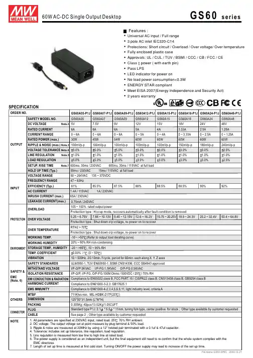
SPECIFICATIONORDER NO.SAFETY MODEL NO.DC VOLTAGE Note.2RATED CURRENTCURRENT RANGERATED POWER(max.)RIPPLE & NOISE (max.)Note.3 OUTPUTSETUP, RISE TIME Note.7HOLD UP TIME(Typ.)VOLTAGE RANGEFREQUENCY RANGEEFFICIENCY(Typ.)AC CURRENTINPUTENVIRONMENT INRUSH CURRENT (max.) LEAKAGE CURRENT(max.)SAFETY STANDARDSSAFETY& EMC (Note. 6)WORKING TEMP. WORKING HUMIDITY STORAGE TEMP., HUMIDITY TEMP. COEFFICIENT VIBRATIONMTBFDIMENSIONOTHERSNOTE PACKINGPROTECTION5VGS60A05GS60A05-P1J GS60A07-P1J GS60A09-P1J GS60A12-P1J GS60A15-P1J GS60A18-P1J GS60A24-P1J GS60A48-P1J7.5VGS60A079VGS60A0912VGS60A1215VGS60A1518VGS60A1824VGS60A2448VGS60A48100mVp-p100mVp-p100mVp-p100mVp-p100mVp-p150mVp-p180mVp-p240mVp-p VOLTAGE TOLERANCE Note.4LINE REGULATION Note.5LOAD REGULATION5.0% 5.0% 5.0% 3.0% 3.0% 3.0% 3.0% 2.5%1.0% 1.0% 1.0% 1.0% 1.0% 1.0% 1.0% 1.0%5.0% 5.0% 5.0% 3.0% 3.0% 3.0% 3.0% 2.5%90 ~ 264VAC 135 ~ 370VDC47 ~ 63Hz81%85.5%87.5%88%88.5%88.5%90%92%1.4A/ 115VAC 1A/ 230VAC65A/ 230VAC0.75mA/ 240VACWITHSTAND VOLTAGEISOLATION RESISTANCEI/P-O/P:3KVAC I/P-FG:1.5KVAC O/P-FG:0.5KVACI/P-O/P, I/P-FG, O/P-FG/ 25/ 70% RH:100M Ohms / 500VDC711Khrs min. MIL-HDBK-217F(25)-10 ~ +50(Refer to output load derating curve)20% ~ 90% RH non-condensing-20 ~ +85, 10 ~ 95% RH0.03% /(0 ~ 50)10 ~ 500Hz, 2G 10min./1cycle, period for 60min.each along X,Y, Z axes125*50*31.5mm (L*W*H)0.305Kg; 40pcs/13.02Kg/1.05CUFTCONNECTOR PLUGCABLEStandard type for stock ther type available by customer requestedP1J: 2.1* 5.5* 11mm, tuning fork type, center positive; OSee page 2ther type available by customer requested; O1. All parameters are specified at 230VAC input, rated load, 2570% RH ambient.2. DC voltage: The output voltage set at point measure by plug terminal & 50% load.3. Ripple & noise are measured at 20MHz by using a 12" twisted pair terminated with a 0.1uf & 47uf capacitor.4. Tolerance: includes set up tolerance, line regulation, load regulation.5. Line regulation is measured from low line to high line at rated load.6. The power supply is considered as an independent unit, but the final equipment still need to re-confirm that the whole system complies with theEMC directives.7. Length of set up time is measured at first cold start. Turning ON/OFF the power supply may lead to increase of the set up time.60W AC-DC Single Output Desktop GS60seriesFeatures :Compliance to EN61000-3-2,3, GB17625.1Compliance to EN61000-4-2,3,4,5,6,8,11, light industry level, criteria AHARMONIC CURRENTEMS IMMUNITYEMI CONDUCTION & RADIATIONOVERLOADOVER VOLTAGEOVER TEMPERATURE105 ~ 150%rated output powerProtection type : Hiccup mode, recovers automatically after fault condition is removedRTH2 > 706A6A6A5A4A 3.33A 2.5A 1.25A0 ~ 6A0 ~ 6A0 ~ 6A0 ~ 4A0 ~ 3.33A0 ~ 2.5A0 ~ 1.25A30W45W54W60W0 ~ 5A60W60W60W60WProtection type : Shut down o/p voltage, re-power on to recoverProtection type : Shut down o/p voltage, re-power on to recoverUL60950-1,TUV EN60950-1, BSMI CNS14336, CCC GB4943approvedCompliance to EN55022 class B, FCC PART15 / CISPR22 class B, CNS13438 class B, GB9254 class BUniversal AC input / Full range3 pole AC inlet IEC320-C14Protections: Short circuit / Overload / Over voltage/ Over temperatureFully enclosed plastic caseApprovals: UL / CUL / TUV / BSMI / CCC / CB / FCC / CEClass power ( with earth pin)Pass LPSLED indicator for power onNo load power consumption<0.3WENERGY STAR compliantMeet EISA 2007(Energy Independence and Security Act)2 years warranty600ms, 30ms / 230VAC 600ms, 30ms / 115VAC at full load50ms / 230VAC 15ms / 115VAC at full load7.88 ~ 10.13V9.45 ~ 12.15V12.6 ~ 16.2V15.75 ~ 20.25V18.9 ~ 24.3V25.2 ~ 32.4V50.4 ~ 64.8V5.25 ~6.75V7010mm110.5mmMechanical SpecificationAMBIENT TEMPERATURE ()L O A D (%)-10201030402040508060100605070INPUT VOLTAGE (VAC) 60Hz9010095120110160140200180240220264L O A D (%)Ta=25901008070605040(HORIZONTAL)Derating CurveStatic Characteristics12531.550UL2624 16AWG UL1185 16AWG 100050mm for 12 ~ 15V 100050mm for 5 ~ 9V UL1185 18AWG 180050mm for 18 ~ 48VPlug AssignmentStandard plug: P1J (option)ID 2.1 x OD 5.5C"+"P/N OUTPUTP1JCENTER+GS60series60W AC-DC Single Output DesktopCase No. 974AUnit:mm。
PT4115介绍

华润矽威科技LED驱动新产品PT4115宽调光比的高亮度LED照明驱动PT4115PT4115#PT4115特点和应用DC-DC降压式LED转换器特点:•输入范围从8V到30V,击穿电压>45V•输出电流高达1.2A,内置大功率MOFET•效率高达97%•超低的关断电流•±5%输出电流精度•LED开路保护•模拟/PWM调光功能选择,高达5000:1的PWM调光比•内部含有抖频特性,有效地改善了EMI应用:MR16射灯、LED装饰照明、汽车的辅助照明灯##•输入电压范围:8-30V •输出电流高达1.2A •外部元器件少•调光特性好,PWM/模拟调光直流输入应用方案直流输入方案PT4115VINCSNSWDIMGNDR S L C INV IND(SS14)47uH10uFDC8-30V0.27ΩLED 1W#12-18VAC 应用方案12-18V AC 输入方案PT4115VINCSNSWDIMGNDR S L C INV IND47uH100uFAC12-18VDC8-30V0.13Ω3W LED#系统效率和输出电流8101214161820222426283075%80%85%90%95%100%E f f i c i e n c ySupply Voltage Vin(V)Efficiency1,3 and 7 LEDsL=47uH Rs=0.13ohm1LED3 LEDs7LEDs510152025307107207307407507607707807908007LEDs3LEDs5LEDs2LEDs6LEDs4LEDsO u t p u t C u r r e n t (m A )Supply Voltage Vin(V)Output Current L=47uH Rcs=0.13ohm1LED 3W LED 输出效率3W LED 输出电流#LED电流随LED个数和输入电压关系510152025301.101.121.141.161.181.201.221.247LEDs6LEDs5LEDs4LEDs3LEDs2LEDsO u t p u t C u r r e n tSupply Voltage(V)Output Current L=27uH Rcs=0.0825ohm1LED510152025302802852902953003053103153203257LEDs6LEDs5LEDs4LEDs1LED2LEDs3LEDsO u t p u t C u r r e n tSupply Voltage (V)Output Current L=100uH Rcs=0.33ohm1.2A 输出电流300mA 输出电流#PWM调光0.00.20.40.60.8 1.00100200300400500600O u t p u t C u r r e n t (u A )Dim Duty CycleOutput Current vs Dim Duty Cycle50KHz20KHz100HzPWM 调光,从0%到100%)55.2%,1000(1.0V V V D RsD I pulse OUT <<≤≤×=)5.25.0%,1000(5.21.0V V V D RsD V I pulse pulse OUT <<≤≤×××=#PWM调光比100,215000:1PWM settle PWM settlef Hz t usDim Range f t == ==´PWM 调光比#012345100200300400500600700800L E D C u r r e n t (u A )Dim Pin Voltage(V)LED Current vs VdimR=0.13ohmR=0.33ohm模拟调光)5.25.0(5.21.0V V V RsV I DIM DIM OUT≤≤××=)55.2(1.0V V V RsI DIM OUT≤≤=模拟调光动态温度调节DIM端内部是一个1兆上拉电阻(Rup)接到内部5V电源。
pt4115大功率恒流应用电路规格书
pt4115大功率恒流应用电路规格书引言:PT4115是一款集成了开关功率MOSFET的电流模式恒流LED驱动芯片。
它能够提供高效率和精确的LED亮度调节功能,广泛应用于室内和室外照明系统。
本文将详细介绍PT4115的规格和应用电路。
1. PT4115的特性和规格1.1 输入电压范围PT4115能够工作在8V至30V的宽输入电压范围内。
这使得它非常适合应用在各种不同类型的电源系统中。
1.2 输出电流调节范围PT4115可以通过外部器件来设置和调节输出电流。
典型的输出电流可在200mA至2A之间进行调节,因此可以满足不同功率要求的LED照明系统。
1.3 高效率和低功耗PT4115内部集成了高效率的开关功率MOSFET,具有较低的导通压降和热耗散。
在应用中,它能够以高效率转换输入电源的能量为输出电流和电压,从而减少能量损耗。
1.4 瞬态保护和过温保护PT4115具有瞬态保护和过温保护功能,能够在输入电源电压波动或工作温度过高时自动保护驱动电路,防止瞬态或长时间过载损坏。
2. PT4115应用电路设计以PT4115为核心的应用电路设计如下:(图示PT4115应用电路示意图)2.1 输入电源电容选取为了确保电路的稳定工作,建议在输入电源端并联一个适当的电容。
这可以有效减小输入电源的纹波和噪音,提供稳定的工作环境。
2.2 输出电流设置通过选择合适的电阻和电流感应器来设置输出电流。
电流感应器的选择要符合输出电流和电路要求,以保证PT4115能够正常工作。
2.3 PWM调光控制PT4115内部集成了一个可调电流比例控制器,通过PWM信号调节LED的亮度。
这可以实现精确的亮度调节和频闪控制,以满足不同应用场景的需求。
3. PT4115应用实例以室内LED照明系统为例,利用PT4115实现恒流驱动LED,具体应用实例如下:(图示PT4115应用实例电路图)3.1 输入电压接入将室内电源与PT4115的输入端相连接,注意输入电压范围应在8V 至30V之间。
PT4115规格参数

C
Note 1: Absolute Maximum Ratings indicate limits beyond which damage to the device may occur. Recommended Operating Range indicates conditions for which the device is functional, but do not guarantee specific performance limits. Electrical Characteristics state DC and AC electrical specifications under particular test conditions which guarantee specific performance limits. This assumes that the device is within the Operating Range. Specifications are not guaranteed for parameters where no limit is given, however, the typical value is a good indication of device performance. Note 2: The maximum power dissipation must be derated at elevated temperatures and is dictated by TJMAX, θJA, and the ambient temperature TA. The maximum allowable power dissipation is PDMAX = (TJMAX - TA)/ θJA or the number given in Absolute Maximum Ratings, whichever is lower. Note 3: Human body model, 100pF discharged through a 1.5kΩ resistor.
PT4115恒流驱动资料书
深圳市森利威尔电子有限公司 联系人:刘先生 手机:13528898767 QQ:2355368873 欢迎咨询,竭诚服务
第 1 页 共 17 页
30V / 1.2A 高调光比 LED 恒流驱动器
PT4115
最大额定值(1)
项目 电源电压 功率开关的漏端 电流采样端(相对 VIN) 开关使能、模拟和 PWM 调光端 功率开关输出电流 功耗(2) 热阻,SOT89-5(θJA) 工作结温范围 储存温度范围
第 4 页 共 17 页
30V / 1.2A 高调光比 LED 恒流驱动器
PT4115
2.5 V,输出 LED 电流保持恒定,并由(0.1 / RS)设定。LED 电流还可以通过 DIM 到地之间接一个 电阻进行调节,内部有一个上拉电阻(典型 1.2 兆欧姆)接在内部稳压电压 5 V 上,DIM 管脚的电 压由内部和外部的电阻分压决定。
(转下页)
深圳市森利威尔电子有限公司 SHENZHEN SENLIWELL ELECTRONICS CO.,LTD
第 8 页 共 17 页
30V / 1.2A 高调光比 LED 恒流驱动器
(接上页)
PT4115
深圳市森利威尔电子有限公司 SHENZHEN SENLIWELL ELECTRONICS CO.,LTD
深圳市森利威尔电子有限公司 SHENZHEN SENLIWELL ELECTRONICS CO.,LTD
第 10 页 共 17 页
30V / 1.2A 高调光比 LED 恒流驱动器
PT4115
IOUT
= 0.1× D RS
(0 ≤ D ≤100 %,2.5 V < VPULSE < 5 V )
如果高电平小于 2.5V,则
PT415
Output Current(uA)
Output Current
Output Current vs Dim Duty Cycle
600
LED Current vs Vdim
800
20KHz
700
500
100Hz
600
R=0.13ohm
LED Current(uA)
400
Micro Bridge Technology Co.,Ltd. 300
Efficiency1,3 and 7 LEDs
100%
L=47uH
Rs=0.13ohm
95%
7LEDs
90%
3 LEDs
85%
80%
1LED
75% 8 10 12 14 16 18 20 22 24 26 28 30
Supply Voltage Vin(V)
Vdim vs Supply Voltage
Ambient Temperature Switch "on" Resistance vs Temp
1.0
Vin=12V
0.9
0.8
0.7
0.6
0.5
0.4 0.3
-50
0
50
100
150
Ambient Temperature
Supply Current vs Supply Voltage
250
200
平均采样电压 采样电压迟滞 CSN管脚输入电流
关断电流
内部电路工作电压 DIM输入高电平 DIM输入低电平 模拟调光电压范围 最大PWM调光频率 低频PWM调光占空比范围 低频PWM调光比
测试条件
pt4115中文资料
PT4115是一个感应降压转换器,工作在连续模式。
当电源电压高于输出电压时,可以有效地驱动单个或多个串联的led。
该集成电路的输入电压范围为5V~24V,输出电流可外调,最大输出电流可达0.7A。
PT4115集成了功率管和高端电流检测电路,平均输出电流可通过外接电阻器设定。
此外,输出电流也可以通过外部调节引脚进行调节,使其低于设定值。
ADJ引脚可接收直流电压或PWM信号,支持线性调光或PWM调光。
如果在ADJ引脚上施加0.2V或更低的电压,输出功率管将关闭,IC将以低电流待机模式工作。
PT4115集成过热软关机功能。
当芯片内部结温升至135℃时,随着结温的不断升高,输出电流逐渐减小。
当结温达到150℃时,输出电流减小到0。
PT4115特性高效率(高达95%)软启动时间可调IC过热软关机最大0.7A输出电流PWM调光/模拟直流调光模拟直流调光范围15%~100%最小10uSPWM调光脉冲宽度(调光频率为1KHz时,调光精度可达1%)宽输入电压范围:5V~24V内置LED开路保护±3%输出电流精度SOT-89-5L套装PT4115引脚图pt4115中文数据汇总(pt4115引脚图及功能-内部结构及应用电路)pt4115,LED驱动,PWM调光PT4115工作原理参照典型的应用电路,PT4115与电感(L1)和电流感测电阻(Rs)一起构成一个工作在连续模式下的自振荡降压电路。
当应用电路第一次通电时,电感器L1和电阻器Rs的初始电流为零。
此时,VIN和ISNS之间没有电压差,ISENSE模块的输出也很低。
这个信号被传递到PWM比较器的负输入端,并且PWM比较器的输出很高。
这会使NMOS打开电源,LX引脚被拉低。
NMOS接通后,电流通过电阻器Rs、LED和电感器L1从VIN流向GND。
电流在RS 上产生一个上升的电压斜坡,上升斜率由VIN,L1和负载决定。
电阻Rs产生的电压降VRS 由ISENSE模块检测,并转换为与ISENSE模块中VRS成比例的输出电压。
PT4115LED光源驱动电路
PT4115LED光源驱动电路LED光源驱动电路LED 光源的驱动电路就是把12V 直流电压变换成稳定的恒流源,电路的设计本着删繁就简、节省成本的原则,应该从能完成这个电路设计要求的众多LED驱动芯片中选择集成度高、性能较好、应用电路简单、价格较平的性价比有优势的芯片。
因此选择驱动电路周边器件少的驱动芯片是生产成本的首要考量。
PT4115 用在1—6W 的白光LED 光源驱动方案时只需要四个零件(图2),图2 PT4115 LED 光源驱动电路Cin 是输入滤波电容,Rs 设定流过LED 的电流IF,Rs=0.1/ILED;L 是续流电感,D5 是续流二极管。
因适配器已提供12V 的直流电压,原图为交流电压输入整流用的桥式整流器D1-D4 可省略。
虽然零件少了但对零件的要求高了,设计时要按表1 提示的要求选用,才能使电路进入良好的工作状态。
PT4115的开关频率采用抖频技术有效降低EMI,省略了抗EMI 电路。
表1 关键元器件的选择LED 光源驱动芯片的恒流精度对于LED 灯具生产厂家而言是至关重要的,目前LED 光源驱动IC 的恒流精度批量生产时都会有一定的离散性,LED 灯具生产厂家在批量生产调试时,同样的电源、同样的LED 光源负载、同样的恒流源电源板,因同一型号的不同驱动IC 其恒流精度的个性差异会导致恒流源电源板输出电流产生一定的公差,会使同一LED 光源负载的发光亮度有所不同,这就会增加恒流源电源板大批量生产时在线调试的时间,影响生产力。
因此,恒流源电源板生产厂家应选用恒流精度高的驱动IC,恒流精度至少要小于±3%,如是±1%更理想,但其价格会高于±3%的产品。
几点关键技术1)电感的选择以3X1W的高亮度白光LED光源的设计案例而言,三个1W的LED光源串联,其工作电流可设计为300-350mA,L的电感量应选用68uH—100uH,Q 值大于50,饱和电流大于800mA 的磁路闭合电感器。