AMS3106AM1-ADJ中文资料
和利时LM可编程控制器硬件手册

第1章从硬件体系结构、编程软件、快速应用等各个方面对LM小型PLC作了概述性介绍。
第2、3章主要针对CPU模块、扩展模块的技术规格、端子定义与接线示意图及等效电路进行 了详细阐述。
目录
第 1 章 概述 .......................................................................................................... 1
1.1 概述................................................................................................................................................... 1 1.2 硬件体系结构................................................................................................................................... 1
本手册仅供商业用户阅读、查询,在未得到北京和利时系统工程股份有限公司特别授权的 情况下,无论出于何种原因和目的,均不得用任何电子或机械方法,以任何形式复制和传递本 手册的内容。否则本公司将依法追究法律责任。
我们已核对本手册中的内容、图表与所述硬件设备相符,但误差难以避免,并不能保证完 全一致,还恳请广大用户批评指正。同时,我们会定期对手册的内容、图表进行检查、修改和 维护,恕不另行通知。
M310A资料
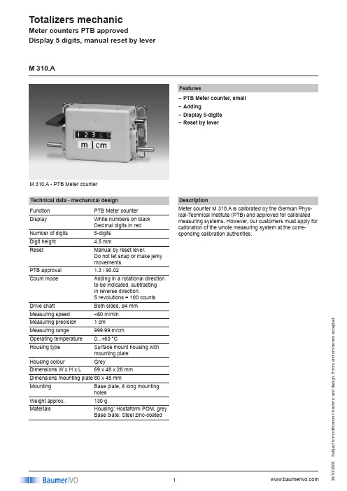
Totalizers mechanicS u b j e c t t o m o d i fi c a t i o n i n t e c h n i c a n d d e s i g n . E r r o r s a n d o m i s s i o n s e x c e p t e d .008M 310.A - PTB Meter counter FeaturesPTB Meter counter, small –Adding –Display 5-digits –Reset by lever–M 310.ATechnical data - mechanical design Function PTB Meter counter DisplayWhite numbers on black Decimal digits in red Number of digits 5-digits Digit height 4.5 mmResetManual by reset lever.Do not let snap or make jerky movements.PTB approval 1.3 / 90.02Count modeAdding in a rotational direction to be indicated, subtracting in reverse direction.5 revolutions = 100 counts Drive shaft Both sides, ø4 mm Measuring speed <60 m/minMeasuring precision 1 cm Measuring range 999.99 m/cm Operating temperature 0...+60 °CHousing type Surface mount housing with mounting plate Housing colour GreyDimensions W x H x L 69 x 48 x 28 mmDimensions mounting plate 80 x 48 mmMounting Base plate, 6 long mounting holes Weight approx.130 gMaterialsHousing: Hostaform POM, grey Base blate: Steel zinc-coatedMeter counters PTB approvedDisplay 5 digits, manual reset by leverMeter counter M 310.A is calibrated by the German Phys-ical-Technical Institute (PTB) and approved for calibrated measuring systems. However, our customers must apply for calibration of the whole measuring system at the corre-sponding calibration authorities.DescriptionTotalizers mechanicS u b j e c t t o m o d i fi c a t i o n i n t e c h n i c a n d d e s i g n . E r r o r s a n d o m i s s i o n s e x c e p t e d .008M 310.APart number M 310.A0Display / direction of rotation15-digits 999.99 m, 5 revolutions= 100 digits / direction I25-digits 999.99 m, 5 revolutions= 100 digits / direction IIMeter counters PTB approvedDisplay 5 digits, manual reset by leverAway from user Towards userSense of rotation I Sense of rotation IIDirection of strokes and rotationDimensionsAccessoriesMeasuring wheels (page %S)MR211.04A Circumf. 20 cm, knurled aluminium MR241.04D Circumf. 20 cm, smooth Hytrel TPE-E MR261.04A Circumf. 20 cm, knopped rubber NBR Nitril MR291.04D Circumf. 20 cm, grooved Hytrel TPE-E。
TLV320AIC3106中文资料

BurrĆBrown Productsfrom TexasInstrumentsFEATURESAPPLICATIONSDESCRIPTIONTLV320AIC3106SLAS509A–DECEMBER2006–REVISED APRIL2007 LOW POWER STEREO AUDIO CODEC FOR PORTABLE AUDIO/TELEPHONY•Power Supplies:•Stereo Audio DAC–Analog:2.7V–3.6V.–102-dBA Signal-to-Noise Ratio–Digital Core:1.525V–1.95V–16/20/24/32-Bit Data–Digital I/O:1.1V–3.6V–Supports Rates From8kHz to96kHz•Packages:5×5mm80-VFBGA;7×7mm48-QFN(Future Product)–3D/Bass/Treble/EQ/De-Emphasis Effects–Flexible Power Saving Modes andPerformance are Available•Digital Cameras•Stereo Audio ADC•Smart Cellular Phones–92-dBA Signal-to-Noise Ratio–Supports Rates From8kHz to96kHz–Digital Signal Processing and NoiseThe TLV320AIC3106is a low power stereo audio Filtering Available During Record codec with stereo headphone amplifier,as well as•Ten Audio Input Pins multiple inputs and outputs programmable insingle-ended or fully differential configurations.–Programmable in Single-Ended or FullyExtensive register-based power control is included, Differential Configurationsenabling stereo48-kHz DAC playback as low as15–3-State Capability for Floating Input mW from a3.3-V analog supply,making it ideal for Configurations portable battery-powered audio and telephonyapplications.•Seven Audio Output Drivers–Stereo Fully Differential or Single-Ended The record path of the TLV320AIC3106contains Headphone Drivers integrated microphone bias,digitally controlled stereomicrophone preamplifier,and automatic gain control –Fully Differential Stereo Line Outputs(AGC),with mix/mux capability among the multiple –Fully Differential Mono Outputanalog inputs.Programmable filters are available •Low Power:15-mW Stereo48-kHz Playback during record which can remove audible noise that With3.3-V Analog Supply can occur during optical zooming in digital cameras.The playback path includes mix/mux capability from •Ultra-Low Power Mode with Passive Analogthe stereo DAC and selected inputs,through Bypassprogrammable volume controls,to the various •Programmable Input/Output Analog Gains outputs.•Automatic Gain Control(AGC)for RecordThe TLV320AIC3106contains four high-power •Programmable Microphone Bias Level output drivers as well as three fully differential output •Programmable PLL for Flexible Clock drivers.The high-power output drivers are capable ofdriving a variety of load configurations,including up Generationto four channels of single-ended16-Ωheadphones •Control Bus Selectable SPI or I2Cusing ac-coupling capacitors,or stereo16-Ω•Audio Serial Data Bus Supports I2S,headphones in a capacitorless output configuration.Left/Right-Justified,DSP,and TDM Modes•Alternate Serial PCM/I2S Data Bus for EasyConnection to Bluetooth™Module•Concurrent Digital Microphone and AnalogMicrophone Support Available•Extensive Modular Power ControlPlease be aware that an important notice concerning availability,standard warranty,and use in critical applications of TexasInstruments semiconductor products and disclaimers thereto appears at the end of this data sheet.MicroStar Junior is a trademark of Texas Instruments.Bluetooth is a trademark of Bluetooth SIG,Inc.UNLESS OTHERWISE NOTED this document contains Copyright©2006–2007,Texas Instruments Incorporated PRODUCTION DATA information current as of publication date.Products conform to specifications per the terms of TexasInstruments standard warranty.Production processing does notnecessarily include testing of all parameters. TLV320AIC3106SLAS509A–DECEMBER2006–REVISED APRIL2007These devices have limited built-in ESD protection.The leads should be shorted together or the device placed in conductive foam during storage or handling to prevent electrostatic damage to the MOS gates.The stereo audio DAC supports sampling rates from8kHz to96kHz and includes programmable digital filtering in the DAC path for3D,bass,treble,midrange effects,speaker equalization,and de-emphasis for32-kHz, 44.1-kHz,and48-kHz rates.The stereo audio ADC supports sampling rates from8kHz to96kHz and is preceded by programmable gain amplifiers or AGC that can provide up to59.5-dB analog gain for low-level microphone inputs.The TLV320AIC3106provides an extremely high range of programmability for both attack (8-1,408ms)and for decay(0.05-22.4seconds).This extended AGC range allows the AGC to be tuned for many types of applications.For battery saving applications where neither analog nor digital signal processing are required,the device can be put in a special analog signal passthru mode.This mode significantly reduces power consumption,as most of the device is powered down during this pass through operation.The serial control bus supports SPI or I2C protocols,while the serial audio data bus is programmable for I2S, left/right-justified,DSP,or TDM modes.A highly programmable PLL is included for flexible clock generation and support for all standard audio rates from a wide range of available MCLKs,varying from512kHz to50MHz, with special attention paid to the most popular cases of12-MHz,13-MHz,16-MHz,19.2-MHz,and19.68-MHz system clocks.The TLV320AIC3106operates from an analog supply of2.7V–3.6V,a digital core supply of1.525V–1.95V, and a digital I/O supply of1.1V–3.6V.The device is available in the5×5-mm,80-ball MicroStar Junior™BGA package and in the future a7×7-mm,48-lead QFN package.2Submit Documentation FeedbackSIMPLIFIED BLOCK DIAGRAMMIC3L / LINE3LHPRCOMHPLCOMD I N O U TC L KC L KHPROUTMIC3R / LINE3RMONO_LOP MONO_LOMMIC2RM / LINE2RMMIC2RP / LINE2RP MIC1RM / LINE1RMMIC1RP / LINE1RP MIC2LM / LINE2LMMIC2LP / LINE2LP MIC1LM / LINE1LMMIC1LP / LINE1LP TLV320AIC3106SLAS509A–DECEMBER 2006–REVISED APRIL 2007PACKAGING/ORDERING INFORMATION (1)PACKAGE OPERATING ORDERING TRANSPORT PRODUCTPACKAGEDESIGNATORTEMPERATURENUMBER MEDIA,QUANTITYRANGETLV320AIC3106IZQE Trays,360ZQETLV320AIC3106IZQERTape and Reel,3000BGA-80N/A Trays,360GQE (Future TLV320AIC3106–40°C to 85°CProduct)N/A Tape and Reel,3000N/A Tape and Reel,250RGZ (Future QFN-48Product)N/ATape and Reel,2000(1)For the most current package and ordering information,see the Package Option Addendum at the end of this document,or see the TI website at .3Submit Documentation FeedbackPINASSIGNMENTSABC D E F G H J 48−lead QFN Package - Future Product(Bottom view)5x5mm 80−Ball BGA Package(Bottom View)4 811 21 32 43 63 7(Not to scale)TLV320AIC3106SLAS509A–DECEMBER 2006–REVISED APRIL 2007Connect QFN thermal pad to DRVSS.The shaded balls on BGA package are not connected to the die,but are electrically connected to each other.TERMINAL FUNCTIONSTERMINALDESCRIPTIONBGA BALLQFN NAME A213MICBIAS Microphone Bias Voltage Output A114MIC3R MIC3Input (Right or Multifunction)C2,D215AVSS_ADC Analog ADC Ground Supply,0VB1,C116,17DRVDD ADC Analog and Output Driver Voltage Supply,2.7V –3.6V D118HPLOUT High-Power Output Driver (Left +)E119HPLCOM High-Power Output Driver (Left –or Multifunctional)E2,F220,21DRVSS Analog Output Driver Ground Supply,0VF122HPRCOM High-Power Output Driver (Right –or Multifunctional)G123HPROUT High-Power Output Driver (Right +)H124DRVDD ADC Analog and Output Driver Voltage Supply,2.7V–3.6V J125AVDD_DAC Analog DAC Voltage Supply,2.7V–3.6V G2,H226AVSS_DAC Analog DAC Ground Supply,0V J227MONO_LOP Mono Line Output (+)J328MONO_LOM Mono Line Output (–)J429LEFT_LOP Left Line Output (+)J530LEFT_LOM Left Line Output (–)J631RIGHT_LOP Right Line Output (+)J732RIGHT_LOM Right Line Output (–)H833RESET ResetGeneral-Purpose Input/Output #2(Input/Output)/Digital Microphone Data Input/PLL Clock J834GPIO2Input/Audio Serial Data Bus Bit Clock Input/Output4Submit Documentation FeedbackTLV320AIC3106SLAS509A–DECEMBER2006–REVISED APRIL2007 TERMINAL FUNCTIONS(continued)TERMINALDESCRIPTIONBGA BALL QFN NAMEGeneral-Purpose Input/Output#1(Input/Output)/PLL/Clock Mux Output/Short Circuit Interrupt J935GPIO1/AGC Noise Flag/Digital Microphone Clock Audio Serial Data Bus Word Clock Input/Output H936DVDD Digital Core Voltage Supply,1.525V–1.95VG837MCLK Master Clock InputG938BCLK Audio Serial Data Bus Bit Clock(Input/Output)F939WCLK Audio Serial Data Bus Word Clock(Input/Output)E940DIN Audio Serial Data Bus Data Input(Input)F841DOUT Audio Serial Data Bus Data Output(Output)D942DVSS Digital Core/I/O Ground Supply,0VE843SELECT Control Mode Select Pin(1=SPI,0=I2C)C944IOVDD I/O Voltage Supply,1.1V–3.6VB845MFP0Multifunction pin#0–SPI Chip Select/GPI/I2C Address Pin#0B946MFP1Multifunction pin#1–SPI Serial Clock/GPI/I2C Address Pin#1SA847MFP2Multifunction pin#2–SPI MISO Slave Serial Data Output/GPOIA948MFP3Multifunction pin#3–SPI MOSI Slave Serial Data Input/GPI/Audio Serial Data Bus Data Input C81SCL I2C Serial Clock/GPIOD82SDA I2C Serial Data Input/Output/GPIOA7–NC No ConnectA63LINE1LP MIC1or Line1Analog Input(Left+or Multifunction)A54LINE1LM MIC1or Line1Analog Input(Left–or Multifunction)B75LINE1RP MIC1or Line1Analog Input(Right+or Multifunction)B66LINE1RM MIC1or Line1Analog Input(Right–or Multifunction)A47LINE2LP MIC2or Line2Analog Input(Left+or Multifunction)B58LINE2LM MIC2or Line2Analog Input(Left–or Multifunction)B49LINE2RP MIC2or Line2Analog Input(Right+or Multifunction)A310LINE2RM MIC2or Line2Analog Input(Right–or Multifunction)B311MIC3L MIC3Input(Left or Multifunction)B212MICDET Microphone DetectC4-C7,D3-D7,E3-E7,–NC Do not connect.F3-F7,G3-G7,H3-H75Submit Documentation FeedbackABSOLUTE MAXIMUM RATINGSDISSIPATION RATINGS (1)RECOMMENDED OPERATING CONDITIONSTLV320AIC3106SLAS509A–DECEMBER 2006–REVISED APRIL 2007over operating free-air temperature range (unless otherwise noted)(1)(2)VALUEUNIT AVDD_DAC to AVSS_DAC,DRVDD to DRVSS,AVSS_ADC –0.3to 3.9V AVDD to DRVSS –0.3to 3.9V IOVDD to DVSS –0.3to 3.9V DVDD to DVSS –0.3to 2.5V AVDD_DAC to DRVDD –0.1to 0.1V Digital input voltage to DVSS –0.3to IOVDD +0.3V Analog input voltage to AVSS_ADC –0.3to AVDD +0.3V Operating temperature range -40to +85°C Storage temperature range-65to +105°C T J MaxJunction temperature 105°CPower dissipation(T J Max –T A )/θJAThermal impedance ,BGA package 63°C/W θJA Thermal impedance,QFN package—°C/W (1)Stresses beyond those listed under absolute maximum ratings may cause permanent damage to the device.These are stress ratings only,and functional operation of the device at these or any other conditions beyond those indicated under recommended operating conditions is not implied.Exposure to absolute-maximum-rated conditions for extended periods may affect device reliability.(2)ESD complicance tested to EIA/JESD22-A114-B and passed.T A =25°C DERATING T A =75°C T A =85°C PACKAGE TYPEPOWER RATINGFACTOR POWER RATINGPOWER RATINGBGA 1.27W 15.9mW/°C476mW 317mW QFN————(1)This data was taken using 2oz.trace and copper pad that is soldered directly to a JEDEC standard 4-layer 3in ×3in PCB.over operating free-air temperature range (unless otherwise noted)MINNOM MAX UNIT AVDD_DAC,Analog supply voltage 2.7 3.3 3.6V DRVDD (1)DVDD (1)Digital core supply voltage 1.525 1.8 1.95V IOVDD (1)Digital I/O supply voltage1.11.8 3.6V V IAnalog full-scale 0-dB input voltage (DRVDD1=3.3V)0.707V RMS Stereo line output load resistance 10k ΩStereo headphone output load resistance 16ΩDigital output load capacitance10pF T A Operating free-air temperature–4085°C(1)Analog voltage values are with respect to AVSS_ADC,AVSS_DAC,DRVSS;digital voltage values are with respect to DVSS.6Submit Documentation FeedbackELECTRICAL CHARACTERISTICSTLV320AIC3106 SLAS509A–DECEMBER2006–REVISED APRIL2007At25°C,AVDD_DAC,DRVDD,IOVDD=3.3V,DVDD=1.8V,Fs=48-kHz,16-bit audio data(unless otherwise noted) PARAMETER TEST CONDITIONS MIN TYP MAX UNITAUDIO ADCInput signal level(0-dB)Single-ended input0.707V RMSSignal-to-noise ratio,Fs=48ksps,0dB PGA gain,Inputs ac-shorted to ground8092dB A-weighted(1)(2)Dynamic range(2)Fs=48ksps,0-dB PGA gain,–60dB full-scale input signal91dBFs=48ksps,0-dB PGA gain,–2dB full-scale1kHz inputTHD Total harmonic distortion–88–70dBsignal217Hz signal applied to DRVDD49 Power supply rejection ratio dB1kHz signal applied to DRVDD46Fs=48ksps,0-dB PGA gain,–2dB full-scale1kHz inputGain error0.84dBsignal1kHz,-2dB Full-scale signal,MIC3L to MIC3R-86Input channel separation1kHz,-2dB Full-scale signal,MIC2L to MIC2R-98dB1kHz,-2dB Full-scale signal,MIC1L to MIC1R-75ADC programmable gain1-kHz input tone59.5dB amplifier maximum gainADC programmable gain0.5dBamplifier step sizeMIC1L/MIC1R inputs routed to single ADC20Input mix attenuation=0dBMIC1L/MIC1R inputs routed to single ADC,input mix80attenuation=12dBMIC2L/MIC2R inputs routed to single ADC20Input mix attenuation=0dBInput resistance kΩMIC2L/MIC2R inputs routed to single ADC,input mix80attenuation=12dBMIC3L/MIC3R inputs routed to single ADC20Input mix attenuation=0dBMIC3L/MIC3R inputs routed to single ADC,input mix80attenuation=12dBInput level control minimum0dB attenuation settingInput level control maximum12dB attenuation settingInput signal level Differential Input 1.414V RMSSignal-to-noise ratio,Fs=48ksps,0dB PGA gain,Inputs ac-shorted to ground,92dB A-weighted(1)(2)Differential ModeFs=48ksps,0-dB PGA gain,–2dB full-scale1kHz inputTHD Total harmonic distortion–91dBsignal,Differential ModeANALOG PASS THROUGH MODEMIC1/LINE1to LINE_OUT330 Input to output switch resistance,Ω(rds ON)MIC2/LINE2to LINE_OUT330ADC DIGITAL DECIMATION FILTER,Fs=48kHzFilter gain from0to0.39Fs±0.1dBFilter gain at0.4125Fs–0.25dBFilter gain at0.45Fs–3dBFilter gain at0.5Fs–17.5dBFilter gain from0.55Fs to64Fs–75dBFilter group delay17/Fs s(1)Ratio of output level with1-kHz full-scale sine-wave input,to the output level with the inputs short circuited,measured A-weighted over a20-Hz to20-kHz bandwidth using an audio analyzer.(2)All performance measurements done with20-kHz low-pass filter and,where noted,A-weighted filter.Failure to use such a filter mayresult in higher THD+N and lower SNR and dynamic range readings than shown in the Electrical Characteristics.The low-pass filter removes out-of-band noise,which,although not audible,may affect dynamic specification values.7Submit Documentation FeedbackTLV320AIC3106SLAS509A–DECEMBER 2006–REVISED APRIL 2007ELECTRICAL CHARACTERISTICS (continued)At 25°C,AVDD_DAC,DRVDD,IOVDD =3.3V,DVDD =1.8V,Fs =48-kHz,16-bit audio data (unless otherwise noted)PARAMETERTEST CONDITIONSMINTYPMAXUNITMICROPHONE BIASProgrammable setting =2.02.0Bias voltage Programmable setting =2.5 2.32.5 2.7VProgrammable setting =DRVDD DRVDDCurrent sourcingProgrammable setting =2.5V4mAAUDIO DAC –Differential Line output,load =10k Ω0-dB Input full-scale signal,output volume control =0-dB,Full-scale output voltage 1.414V RMS Output common mode setting =1.35VSignal-to-noise ratio,No input signal,output volume control =0-dB,Output 90102dB A-weighted (3)common mode setting =1.35V,Fs =48kHz–60dB 1kHz input full-scale signal,output volume control =Dynamic range,A-weighted 99dB 0-dB,Output common mode setting =1.35V,Fs =48kHz 0dB 1kHz input full-scale signal,output volume control =Total harmonic distortion –94–75dB 0-dB,Output common mode setting =1.35V,Fs =48kHz 217Hz Signal applied to DRVDD,AVDD_DAC 77Power supply rejection ratio dB 1kHz Signal applied to DRVDD,AVDD_DAC73DAC channel separation 0-dB Full-scale input signal between left and right Lineout 123dB 0dB 1kHz input full-scale signal,output volume control =DAC Gain Error–0.4dB0-dB,Output common mode setting =1.35V,Fs =48kHz AUDIO DAC -SINGLE ENDED LINE OUTPUT,Load =10k Ω0-dB Input full-scale signal,output volume control =0-dB,Full-scale output voltage 0.707Vrms Output common mode setting =1.35VNo input signal,output volume control =0-dB,Output Signal-to-noise ratio,A-weighted 97dB common mode setting =1.35V,Fs =48kHz0dB 1kHz input full-scale signal,output volume control =Total harmonic distortion 84dB 0-dB,Output common mode setting =1.35V,Fs =48kHz 0dB 1kHz input full-scale signal,output volume control =DAC Gain Error0.55dB0-dB,Output common mode setting =1.35V,Fs =48kHz AUDIO DAC -SINGLE ENDED HEADPHONE OUTPUT,Load =16k Ω0-dB Input full-scale signal,output volume control =0-dB,Full-scale output voltage0.707Vrms Output common mode setting =1.35VNo input signal,output volume control =0-dB,Output 95dB common mode setting =1.35V,Fs =48kHzSignal-to-noise ratio,A-weightedNo input signal,output volume control =0-dB,Output common mode setting =1.35V,Fs =48kHz,50%DAC 96dB Current Boost Mode–60dB 1kHz input full-scale signal,output volume control =Dynamic range,A-weighted 92dB 0-dB,Output common mode setting =1.35V,Fs =48kHz 0dB 1kHz input full-scale signal,output volume control =Total harmonic distortion -80-65dB 0-dB,Output common mode setting =1.35V,Fs =48kHz 217Hz Signal applied to DRVDD,AVDD_DAC 41Power supply rejection ratio dB 1kHz Signal applied to DRVDD,AVDD_DAC44DAC channel separation 0-dB Full-scale input signal between left and right Lineout 84dB 0dB 1kHz input full-scale signal,output volume control =DAC Gain Error-0.5dB0-dB,Output common mode setting =1.35V,Fs =48kHz AUDIO DAC -LINEOUT AND HEADPHONE OUT DRIVERSFirst option1.35Second option 1.5Output common modeVThird option 1.65Fourth option1.8Output volume control max 9dB settingOutput volume control step size1dB (3)Unless otherwise noted,all measurements use output common-mode voltage setting of 1.35V,0-dB output level control gain,16-Ωsingle-ended load.8Submit Documentation FeedbackTLV320AIC3106 SLAS509A–DECEMBER2006–REVISED APRIL2007ELECTRICAL CHARACTERISTICS(continued)At25°C,AVDD_DAC,DRVDD,IOVDD=3.3V,DVDD=1.8V,Fs=48-kHz,16-bit audio data(unless otherwise noted) PARAMETER TEST CONDITIONS MIN TYP MAX UNIT DAC DIGITAL INTERPOLATION–FILTER Fs=48-kspsPassband00.45×Fs Hz Passband ripple±0.06dB Transition band0.45×Fs0.55×Fs Hz Stopband0.55×Fs7.5×Fs Hz Stopband attenuation65dB Group delay21/Fs s DIGITAL I/O0.3×V IL Input low level–0.3VIOVDD0.7×IOVDD>1.6VIOVDDV IH Input high level(4)VIOVDD<1.6V 1.10.1×V OL Output low level VIOVDD0.8×V OH Output high level VIOVDDPOWER CONSUMPTION,DRVDD,AVDD_DAC=3.3V,DVDD=1.8V,IOVDD=3.3VIDRVDD+IAVDD_DAC0.1RESET Held lowµAIDVDD0.2IDRVDD+IAVDD_DAC 2.1Mono ADC record,Fs=8ksps,mAI2S Slave,AGC Off,No signalIDVDD0.5IDRVDD+IAVDD_DAC 4.1Stereo ADC record,Fs=8ksps,mAI2S Slave,AGC Off,No signalIDVDD0.6IDRVDD+IAVDD_DAC Stereo ADC record,Fs=48 4.3ksps,I2S Slave,AGC Off,No mAIDVDD 2.5signalIDRVDD+IAVDD_DAC Stereo DAC Playback to Lineout, 3.5Analog mixer bypassed Fs=48mAIDVDD 2.3ksps,I2S SlaveIDRVDD+IAVDD_DAC Stereo DAC Playback to Lineout, 4.9Fs=48ksps,I2S Slave,No mAIDVDD 2.3signalIDRVDD+IAVDD_DAC Stereo DAC Playback to stereo 6.7single-ended headphone,Fs=48mAIDVDD 2.3ksps,I2S Slave,No signalIDRVDD+IAVDD_DAC 3.1Stereo LINEIN to stereomALINEOUT,No signalIDVDD0IDRVDD+IAVDD_DAC 1.4Extra power when PLL enabled mAIDVDD0.9IDRVDD+IAVDD_DAC28All blocks powered down,µAHeadset detedtion enabledIDVDD2(4)When IOVDD<1.6V,minimum VIH is1.1V.9Submit Documentation FeedbackAUDIO DATA SERIAL INTERFACE TIMINGDIAGRAMWCLKTIMING CHARACTERISTICS(1)TLV320AIC3106SLAS509A–DECEMBER 2006–REVISED APRIL 2007Figure 1.I 2S/LJF/RJF Timing in Master ModeAll specifications typical at 25°C,DVDD =1.8VIOVDD =1.1V IOVDD =3.3V PARAMETERUNIT MINMAX MINMAX t d (WS)ADWS/WCLK delay time5015ns t d (DO-WS)ADWS/WCLK to DOUT delay time 5020ns t d (DO-BCLK)BCLK to DOUT delay time 5015ns t s (DI)DIN setup time 106ns t h (DI)DIN hold time 106ns t r Rise time 3010ns t f Fall time3010ns(1)All timing specifications are measured at characterization but not tested at final test.Figure 2.DSP Timing in Master Mode10Submit Documentation FeedbackTIMING CHARACTERISTICS (1)SLAS509A–DECEMBER 2006–REVISED APRIL 2007All specifications typical at 25°C,DVDD =1.8VIOVDD =1.1V IOVDD =3.3V PARAMETERUNIT MINMAX MINMAX t d (WS)ADWS/WCLK delay time 5015ns t d (DO-BCLK)BCLK to DOUT delay time 5015ns t s (DI)DIN setup time 106ns t h (DI)DIN hold time 106ns t r Rise time 3010ns t f Fall time3010ns(1)All timing specifications are measured at characterization but not tested at final test.Figure 3.I 2S/LJF/RJF Timing in Slave ModeTIMING CHARACTERISTICS (1)(DI)TIMING CHARACTERISTICS (1)SLAS509A–DECEMBER 2006–REVISED APRIL 2007All specifications typical at 25°C,DVDD =1.8VIOVDD =1.1V IOVDD =3.3V PARAMETERUNIT MIN MAXMIN MAXt H (BCLK)BCLK high period 7035ns t L (BCLK)BCLK low period 7035ns t s (WS)ADWS/WCLK setup time 106ns t h (WS)ADWS/WCLK hold time106ns t d (DO-WS)ADWS/WCLK to DOUT delay time (for LJF Mode only)3525ns t d (DO-BCLK)BCLK to DOUT delay time 5020ns t s (DI)DIN setup time 106ns t h (DI)DIN hold time 106ns t r Rise time 84ns t f Fall time84ns(1)All timing specifications are measured at characterization but not tested at final test.Figure 4.DSP Timing in Slave ModeAll specifications typical at 25°C,DVDD =1.8VIOVDD =1.1V IOVDD =3.3V PARAMETERUNIT MIN MAXMIN MAXt H (BCLK)BCLK high period 7035ns t L (BCLK)BCLK low period 7035ns t s (WS)ADWS/WCLK setup time 108ns t h (WS)ADWS/WCLK hold time 108ns t d (DO-BCLK)BCLK to DOUT delay time5020ns t s (DI)DIN setup time 106ns t h (DI)DIN hold time 106ns t r Rise time 84ns t f Fall time84ns(1)All timing specifications are measured at characterization but not tested at final test.TYPICAL CHARACTERISTICS-40020406080100Headphone Out Power - mW T H D - T o t a l H a r m o n i c D i s t o r t i o n - d B51015202530354045ADC, PGA - Setting - dBS N R - S i g n a l -T o -N o i s e - d B1.522.533.54-60-40-20020406080100T - Free-Air Temperature - °CA M I CB I A S V O L T A G E - V1.522.533.542.72.93.1 3.3 3.5V - Supply Voltage - VDD M I C B I A S - VV O L T A G E SLAS509A–DECEMBER 2006–REVISED APRIL 2007TOTAL HARMONIC DISTORTIONSIGNAL-TO-NOISE RATIOvsvsHEADPHONE OUT POWERADC PGA SETTINGFigure 5.Figure 6.MICBIAS VOLTAGEMICBIAS VOLTAGEvsvsSUPPLY VOLTAGEFREE-AIR TEMPERATUREFigure 7.Figure 8.-160-140-120-100-80-60-40-20001234567891011121314151617181920f - Frequency - kHzA m p l i t u d e - dB-160-140-120-100-80-60-40-20001234567891011121314151617181920f - Frequency - kHzA m p l i t u d e - dB-160-140-120-100-80-60-40-20001234567891011121314151617181920f - Frequency - kHzA m p l i t u d e - dBSLAS509A–DECEMBER 2006–REVISED APRIL 2007TYPICAL CHARACTERISTICS (continued)LEFT DAC FFTFigure 9.RIGHT DAC FFTFigure 10.LEFT ADC FFTFigure 11.-160-140-120-100-80-60-40-20001234567891011121314151617181920f - Frequency - kHzA m p l i t u d e - dBSLAS509A–DECEMBER 2006–REVISED APRIL 2007TYPICAL CHARACTERISTICS (continued)RIGHT ADC FFTFigure 12.TYPICAL CIRCUIT CONFIGURATIONµFSLAS509A–DECEMBER 2006–REVISED APRIL 2007TYPICAL CHARACTERISTICS (continued)Figure 13.Typical Connections for Capless Headphone and External Speaker AmpOVERVIEWHARDWARE RESETDIGITAL CONTROL SERIAL INTERFACESPI CONTROLMODERA(6)RA(5)RA(0)D(7)D(6)D(0)7-bit Register AddressWrite8-bit Register DataSSSCLKMOSIMISOHi-ZHi-ZHi-ZHi-ZSLAS509A–DECEMBER 2006–REVISED APRIL 2007The TLV320AIC3106is a highly flexible,low power,stereo audio codec with extensive feature integration,intended for applications in smartphones,PDAs,and portable computing,communication,and entertainment applications.Available in a 5x5mm 80-ball BGA (with 51balls actually used)and 7x7mm 48-lead QFN,the product integrates a host of features to reduce cost,board space,and power consumption in space-constrained,battery-powered,portable applications.The TLV320AIC3106consists of the following blocks:•Stereo audio multi-bit delta-sigma DAC (8kHz–96kHz)•Stereo audio multi-bit delta-sigma ADC (8kHz–96kHz)•Programmable digital audio effects processing (3-D,bass,treble,mid-range,EQ,notch filter,de-emphasis)•Six audio inputs•Four high-power audio output drivers (headphone drive capability)•Three fully differential line output drivers •Fully programmable PLL•Headphone/headset jack detection with interruptCommunication to the TLV320AIC3106for control is pin-selectable (using the SELECT pin)as either SPI or I 2C.The SPI interface requires that the Slave Select signal (MFP0)be driven low to communicate with the TLV320AIC3106.Data is then shifted into or out of the TLV320AIC3106under control of the host microprocessor,which also provides the serial data clock.The I 2C interface supports both standard and fast communication modes,and also enables cascading of up to four multiple codecs on the same I 2C bus through the use of two pins for addressing (MFP0,MFP1).The TLV320AIC3106requires a hardware reset after power-up for proper operation.After all power supplies are at their specified values,the RESET pin must be driven low for at least 10ns.If this reset sequence is not performed,the 'AIC3106may not respond properly to register reads/writes.The TLV320AIC3106control interface supports SPI or I 2C communication protocols,with the protocol selectable using the SELECT pin.For SPI,SELECT should be tied high;for I 2C,SELECT should be tied low.It is not recommended to change the state of SELECT during device operation.Figure 14.SPI WriteRA(6)RA(5)RA(0)Don’t Care7-bit Register AddressRead8-bit Register DataSSSCLKMOSIMISO Hi-ZHi-ZD(7)D(6)D(0)Hi-ZHi-ZSPI COMMUNICATION PROTOCOLSLAS509A–DECEMBER 2006–REVISED APRIL 2007OVERVIEW (continued)Figure 15.SPI ReadIn the SPI control mode,the TLV320AIC3106uses the pins MFP0=SSB,MFP1=SCLK,MFP2=MISO,MFP3=MOSI as a standard SPI port with clock polarity setting of 0(typical microprocessor SPI control bit CPOL =0).The SPI port allows full-duplex,synchronous,serial communication between a host processor (the master)and peripheral devices (slaves).The SPI master (in this case,the host processor)generates the synchronizing clock (driven onto SCLK)and initiates transmissions.The SPI slave devices (such as the TLV320AIC3106)depend on a master to start and synchronize transmissions.A transmission begins when initiated by an SPI master.The byte from the SPI master begins shifting in on the slave MOSI pin under the control of the master serial clock (driven onto SCLK).As the byte shifts in on the MOSI pin,a byte shifts out on the MISO pin to the master shift register.The TLV320AIC3106interface is designed so that with a clock phase bit setting of 1(typical microprocessor SPI control bit CPHA =1),the master begins driving its MOSI pin and the slave begins driving its MISO pin on the first serial clock edge.The SSB pin can remain low between transmissions;however,the TLV320AIC3106only interprets the first 8bits transmitted after the falling edge of SSB as a command byte,and the next 8bits as a data byte only if writing to a register.Reserved register bits should be written to their default values.The TLV320AIC3106is entirely controlled by registers.Reading and writing these registers is accomplished by the use of an 8-bit command,which is sent to the MOSI pin of the part prior to the data for that register.The command is constructed as shown in Table X.The first 7bits specify the register address which is being written or read,from 0to 127(decimal).The command word ends with an R/W bit,which specifies the direction of data flow on the serial bus.In the case of a register write,the R/W bit should be set to 0.A second byte of data is sent to the MOSI pin and contains the data to be written to the register.Reading of registers is accomplished in similar fashion.The 8-bit command word sends the 7-bit register address,followed by R/W bit =1to signify a register read is occurring,.The 8-bit register data is then clocked out of the part on the MISO pin during the second 8SCLK clocks in the frame.Command WordBit 7Bit 6Bit 5Bit 4Bit 3Bit 2Bit 1Bit 0ADDR6ADDR5ADDR4ADDR3ADDR2ADDR1ADDR0R/WThe register map of the TLV320AIC3106actually consists of multiple pages of registers,with each page containing 128registers.The register at address zero on each page is used as a page-control register,and writing to this register determines the active page for the device.All subsequent read/write operations will access the page that is active at the time,unless a register write is performed to change the active page.Only two pages of registers are implemented in this product,with the active page defaulting to page 0upon device reset.For example,at device reset,the active page defaults to page 0,and thus all register read/write operations for。
.3090A;.3070A;.3070A35;.3090A35;中文规格书,Datasheet资料

Hazardous LocationIndustrial VRS Magnetic Speed SensorsDESCRIPTIONHazardous Location VRS sensors are designed for use in locations where explosion-proof or intrinsically safe sensors are required.Passive VRS (Variable Reluctance Speed) Magnetic Speed sensors are simple, rugged devices that do not require an external voltage source for operation.A permanent magnet in the sensor establishes a fixedmagnetic field. The approach and passing of a ferrous metal target near the sensor’s pole piece (sensing area) changes the flux of the magnetic field, dynamically changing its strength. This change in magnetic field strength induces a current into a coil winding which is attached to the output terminals.The output signal of a VRS sensor is an ac voltage that varies in amplitude and wave frequency as the speed of themonitored device changes, and is usually expressed in peak to peak voltage (Vp-p).One complete waveform (cycle) occurs as each target passes the sensor’s pole piece . If a standard gear were used as a target, this output signal would resemble a sine wave if viewed on an oscilloscope.Honeywell also offers VRS sensors for general purpose, high output, power output, high resolution and high temperature, as well as low-cost molded versions.FEATURESSelf-powered operationDirect conversion of actuator speed to output frequencySimple installationNo moving partsDesigned for use over a wide range of speedsAdaptable to a wide variety of configurationsCustomized VRS products for unique speed sensingapplicationsHousing diameters: 3/4 in, 5/8 inHousing material/style: stainless steel threadedTerminations: MS3106 connector, preleaded Output voltages: 30 Vp-p to 60 Vp-pPOTENTIAL APPLICATIONSEngine RPM (revolutions per minute) measurement on aircraft, automobiles, boats, buses, trucks and railvehiclesMotor RPM on oil and gas drilling equipment andmachineryMotor RPM measurement on drills, grinders, lathes andautomatic screw machinesProcess speed measurement on food, textile, paper, woodworking, printing, tobacco and pharmaceuticalindustry machineryMotor speed measurement of electrical generating equipment in grain elevators, sawmills and otherpotentially explosive environmentsSpeed measurement of pumps, blowers, mixers, exhaust Gear speed measurementHazardous Location2 /sensing3/4 INCH EXPLOSION-PROOF SENSORS (All dimensions for reference only. mm/[in])When properly installed using the explosion containment method, all 3070X and catalog listings on this page are certified for use in hazardous locations as follows: Class I, Groups A, B, C, D; Class II Groups E, F, G; Class III.These catalog listings have been tested to and meet the requirements of applicable U.S. and Canadian specifications for the locations described above.Industrial VRS Magnetic Speed SensorsHoneywell Sensing and Control 35/8 INCH EXPLOSION-PROOF SENSORS (All dimensions for reference only. mm/[in])When properly installed using the explosion containment method, the 3090X catalog listings on this page are certified for use in hazardous locations as follows: Class I, Groups A, B, C, D; Class II Groups E, F, G; Class III.These catalog listings have been tested to and meet the requirements of applicable U.S. and Canadian specifications for the locations described above.The catalog listings on this page conform to standards: II 3 G EEx nA II T6.Hazardous Location4/sensing5/8 INCH (M16*) INTRINSICALLY SAFE VRS SENSORS (All dimensions for reference only. mm/[in]) *Contact Honeywell for availability of metric mounting thread versions.When properly installed using the intrinsic safety protection method connected per the control drawings on pages 6 and 7, catalog listings 3042A is intrinsically safe for hazardous locations as follows:Class I, Groups A, B, C, D.This product has been tested to and meets the requirements of applicable U.S. and Canadian specifications for the locations described above.‘Industrial VRS Magnetic Speed SensorsHoneywell Sensing and Control 55/8 INCH (M16*) INTRINSICALLY SAFE VRS SENSORS (All dimensions for reference only. mm/[in]) *Contact Honeywell for availability of metric mounting thread versions.When properly installed using the intrinsic safety protection method connected per the control drawings on pages 6 and 7, catalog listing 3042H20 is intrinsically safe for hazardous locations as follows:Class I, Groups A, B, C, D; Class II Groups E, F, G; Class III.This product has been tested to and meets the requirements of applicable U.S. and Canadian specifications for the locations described above.Hazardous Location6 /sensingHAZARDOUS LOCATIONS Catalog listing 3042H20: Class I, Groups A, B, C, D Class II, Groups E, F, G Class IIICatalog listing 3042A: Class I, Groups A, B, C, DENTITY PARAMETERSVmax = 24 V, Imax = 35 mA, Li = 26 mH, Ci = 0 μF Any barrier (see General Notes) with entity parameters connected in accordance with barrier manufacturers instructions of: Vmax > Voc Ca > Ci + cable capacitance Imax > Isc La > Li + cable inductanceSYSTEM PARAMETERSAny barrier (see General Notes) having one of the following specified parameters: GENERAL NOTES1. For jurisdictions requiring certification to the applicableCanadian standards, the barrier must be CSA Certified and the system must be installed in accordance with the Canadian Electrical Code Part 1.2. For jurisdictions requiring certification to the applicableOccupational Safety and Health Administration (OSHA) standards, the barrier must be CSA NRTL or equivalent and the system must be installed in accordance with the National Electrical Code (NEC), article 504 or ANSI/NFPA 70.SENSOR GROUNDINGCatalog listing 3042A: Sensor housing must be connected to intrinsically safe system ground during installation.Catalog listing 3042H20: Green wire must be connected to intrinsically safe system ground.Exia = Intrinsically Safe, Sécurité IntrinsèqueIndustrial VRS Magnetic Speed SensorsHoneywell Sensing and Control 7.HAZARDOUS LOCATIONS Catalog listing 3042H20: Class I, Groups A, B, C, D Class II, Groups E, F, G Class IIICatalog listing 3042A: Class I, Groups A, B, C, DENTITY PARAMETERSVmax = 24 V, Imax = 35 mA, Li = 26 mH, Ci = 0 μF Any barrier (see General Notes) with entity parameters connected in accordance with barrier manufacturers instructions of: Vmax > Voc Ca > Ci + cable capacitance Imax > Isc La > Li + cable inductanceSYSTEM PARAMETERSAny barrier (see General Notes) having one of the following specified parameters:GENERAL NOTES1. For jurisdictions requiring certification to the applicableCanadian standards, the barrier must be CSA Certified and the system must be installed in accordance with the Canadian Electrical Code Part 1.2. For jurisdictions requiring Certification to the applicableOccupational Safety and Health Administration (OSHA) standards, the barrier must be CSA NRTL or equivalent and the system must be installed in accordance with the National Electrical Code (NEC), article 504 or ANSI/NFPA 70.SENSOR GROUNDINGCatalog listing 3042A: Sensor housing must be connected to intrinsically safe system ground during installation.Catalog listing 3042H20: Green wire must be connected to intrinsically safe system ground.Exia = Intrinsically Safe, Sécurité IntrinsèqueSensing and Control Honeywell1985 Douglas Drive NorthGolden Valley, MN 55422 005879-2-ENMarch 2012Copyright © 2012 Honeywell International Inc. All rights reserved.PERSONAL INJURYWARRANTY/REMEDYHoneywell warrants goods of its manufacture as being free of defective materials and faulty workmanship. Honeywell’s standard product warranty applies unless agreed to otherwise by Honeywell in writing; please refer to your order acknowledgement or consult your local sales office for specific warranty details. If warranted goods are returned to Honeywell during the period of coverage, Honeywell will repair or replace, at its option, without charge those items it finds defective. The foregoing is b uyer’s sole remedy and is in lieu of all other warranties, expressed or implied, including those of merchantability and fitness for a particular purpose. In no event shall Honeywell be liable for consequential, special, or indirect damages.While we provide application assistance personally, through our literature and the Honeywell web site, it is up to the customer to determine the suitability of the product in the application.Specifications may change without notice. The information we supply is believed to be accurate and reliable as of this printing. However, we assume no responsibility for its use.WARNINGMISUSE OF DOCUMENTATIONThe information presented in this product sheet is forComplete installation, operation, and maintenanceSALES AND SERVICEHoneywell serves its customers through a worldwide network of sales offices, representatives and distributors. For application assistance, current specifications, pricing or name of the nearest Authorized Distributor, contact your local sales office or:E-mail: info.sc@Internet: /sensingPhone and Fax:Asia Pacific +65 6355-2828+65 6445-3033 FaxEurope +44 (0) 1698 481481+44 (0) 1698 481676 FaxLatin America +1-305-805-8188+1-305-883-8257 FaxUSA/Canada +1-800-537-6945+1-815-235-6847+1-815-235-6545 Fax分销商库存信息:HONEYWELL.3090A.3070A.3070A35 .3090A35。
MS3106K16S中文资料
FINISHES
Shell - Olive drab over cadmium plate Contacts - Silver plate
MECHANICAL FEATURES
Shell Size - In sixteenths of an inch Coupling - Threaded Contact Arrangements - See pages 216-217
MS-K
tacts; thermocouple contacts must be orderd separately and are solder type unless otherwise requested on order. Cavities that will contain the thermocouple contacts and contact material must be specified when ordering.
• Receptacles in size 10SL are available with pin inserts only. Part Number MS3100K8S-*†
* Add contact arrangment. See pages 216-217. A Thread 1/2-28UNEF-2A 5/8-24UNEF-2A 3/4-20UNEF-2A 7/8-20UNEF-2A 1-20UNEF-2A 1-20UNEF-2A 1-1/8-18UNEF-2A 1-1/4-18UNEF-2A 1-3/8-18UNEF-2A 1-1/2-18UNEF-2A 1-3/4-18UNS-2A 2-18UNS-2A 2-1/4-16UN-2A
Sபைடு நூலகம்(TYP.)
三星 SSD_Magician 中文指导手册

三星SSD Magician 用户手册版权 ©三星电子有限公司本资料版权归三星电子所有。
未经授权严禁复制、使用、分发本资料的全部或部分内容,违者必究。
三星电子保留随时更改资料中关于规格参数的相关内容的权力,如有更改,恕不另行通知。
本资料中由三星电子提供的相关内容,在印刷时视为准确无误,但是三星电子不对此处提到的相关内容进行任何明示或暗示的承诺。
商标及服务条款三星标志为三星电子的注册商标。
Adobe 是一个注册商标,Adobe Acrobat是Adobe公司的注册商标。
其他公司和产品名称均为各自相关公司的注册商标。
目录第 1 章 (5)1.1产品概览.......................................................................................................................................................... .. (6)简介 ........................................................................................................................................................................ (6)注意事项 (6)系统需求....................................................................................................................................................... . (6)第 2 章................................................................................................................................................ . (8)2.1如何使用三星SSD M AGICIAN................................................................................................................... (9)三星SSD Magician安装............................................................................................................................ (9)三星SSD Magician 基本情况 (10)系统信息.................................................................................................................................................. (11)性能基准测试............................................................................................................................................ .. (12)性能优化..................................................................................................................................... ...... ...... .. (13)操作系统优化 (15)固件升级 (16)安全擦除 (17)超容量缓存 (18)磁盘备份 (19)网站链接 (20)第 3 章............................................................................................................................................... (21)3.1固件升级基础............................................................................................................................................. ...... ...... . (22)简介 (22)注意事项 (22)系统需求.......................................................................................................................................... ...... . (23)3.2 W INDOWS系统固件升级........................................................................................................................................ (24)利用Windows系统固件工具升级固件................................................................ ........................................ . (24)3.3 DOS系统固件升级工具基础...................................................................................................... .. (27)为固件升级创建启动盘................................................................................................ .......... .......... .......... . (27)3.4利用DOS工具升级固件................................................................................................... .......... .......... .......... .. (33)DOS固件工具使用......................................................................................................................... .......... . (33)第 4 章............................................................................................................................................... . (37)4.1安全擦除基础.................................................................................................................................................... (38)简介 (38)注意事项 (38)系统需求.................................................................................................................................................... . (39)4.2 W INDOWS系统安全擦除............................................................................................................................... .......... .. (40)4.3准备DOS系统安全擦除工具................................................................................................ ............................ . 41创建含有安全擦除工具的DOS启动USB驱动........................................... ............................ (41)4.4安全擦除工具使用............................................................................................................................. .. (44)启动DOS SSD 应用 (44)第 5 章............................................................................................................................................... (47)5.1局限性 (48)一般局限性 (48)固件升级工具局限性....................................................................................................................... .. (48)安全擦除工具局限性 (48)附件 ................................................................................................................................................ . (50)6.1附件 (51)故障检修 (51)固件升级工具................................................................................................................................................................... .. (51)安全擦除工具 (52)专业词汇................................................................................................................................................. (54)7.1专业词汇 (55)第1章准备1.1 产品概览简介―三星SSD Magician‖ 软件 (以下称SSD Magician)操作简单,适用于台式机或笔记本电脑相连的三星SSD产品。
思博特 条码打印机G-3106

G系列用户手册声明此为A级产品,在生活环境中,该产品可能会造成无线电干扰。
在这种情况下,可能需要用户对其干扰采取切实可行的措施。
商标ARM是Advanced RISC Machines Ltd.的注册商标。
Centronics是Centronics Data Computer Corporation的注册商标。
Microsoft, Windows是Microsoft Corporation的注册商标。
POSTEK是深圳市博思得科技发展有限公司的注册商标。
PS/2是International Business Machines Corporation的注册商标。
版权版权所有2004-2011深圳市博思得科技发展有限公司保留一切版权。
G系列标签打印机用户手册。
二○一一年二月第十版。
免除责任声明本手册在其出版时,确切地阐述了POSTEK G系列G-2108、G-3106、G-2108D、G-3106D四个型号标签打印机的规格和使用说明。
但是其后生产的打印机的规格以及配置可能会在没有任何通告的情况下改变。
该产品的制造商和经销商对于由本手册和打印机之间存在的差异甚至错误所造成的直接或间接的损失不承担任何责任。
尽管本手册对可能发生的问题进行了尽可能详尽的描述,但是不保证实际使用该打印机的过程中仍有未预见的情况发生。
对于使用该打印机中发生的诸如打印机不工作、打印的内容缺损或不清晰等问题,该产品的制造商和经销商只负责排除该打印机的故障(依照保修卡上的保修条款),而对于其它任何直接或间接的损失包括商业利益损失、业务中断损失、商业信息丢失或其它财务损失等不承担责任。
iG系列用户手册重要安全事项在没有该产品制造商授权人员指导下,严禁私自拆装这台打印机及其电源适配器,否则可能会发生触电、打印机的传动机构伤人或损坏机器零部件的事故。
严禁使用损坏的或破旧的电源线,否则可能会造成触电或引发火灾。
严禁过度弯曲、用力拉扯电源线。
TPA3106D1中文资料
APPLICATIONS
• Televisions • Powered Speakers
DESCRIPTION
The TPA3106D1 is a 40-W efficient, Class-D audio power amplifier for driving bridged-tied stereo speakers. The TPA3106D1 can drive stereo speakers as low as 4Ω. The high efficiency, ~92%, of the TPA3106D1 eliminates the need for an external heat sink when playing music.
SHUTDOWN, MUTE GAIபைடு நூலகம்0, GAIN1, INN, INP, MSTR/SLV, SYNC
Continuous total power dissipation
Operating free-air temperature range Operating junction temperature range(2)
TA ≤ 25°C 3.57 W
DERATING FACTOR 29 mW/°C(2)
TA = 70°C 2.29 W
TA = 85°C 1.86 W
(1) For the most current package and ordering information, see the Package Option Addendum at the end of this document, or see the TI Web site at . See TI Technical Briefs SCBA017D and SLUA271 for more information about using the QFN thermal pad.
- 1、下载文档前请自行甄别文档内容的完整性,平台不提供额外的编辑、内容补充、找答案等附加服务。
- 2、"仅部分预览"的文档,不可在线预览部分如存在完整性等问题,可反馈申请退款(可完整预览的文档不适用该条件!)。
- 3、如文档侵犯您的权益,请联系客服反馈,我们会尽快为您处理(人工客服工作时间:9:00-18:30)。
元器件交易网Advanced Monolithic SystemsFEATURES• 0.6V to 6V in 100mV increments Voltages Available • Active High On/Off Control • Output Current of 500mA • Quiescent Current of <1µA when in Shutdown • Low Dropout Voltage of 250mV at 500mA • Wide Supply Voltage Range 1.5V to 15V • Short Circuit and Thermal Protection • Power Good function option • Ceramic Output Capacitor OK • Reference bypass for low noiseAMS3106500mA LOW DROPOUT VOLTAGE REGULATORRoHS compliantAPPLICATIONS• Battery Powered Systems • Cellular Phones • Cordless Telephones • Portable (Notebook) Computers • Portable Instrumentation • Portable Consumer Equipment • Personal Communication Equipment • Radio Control Systems • Low Voltage Systems • MP3 PlayerGENERAL DESCRIPTIONThe AMS3106 is a 500mA low dropout fixed voltage regulator, featuring an internal electronic switch controlled by TTL or CMOS logic levels. When the Enable pin is pulled to a logic high level, the device is in the ON state. Designed specifically for battery powered applications where low quiescent current, low dropout and low standby current are required, the AMS3106 is ideal to use in standby power systems. Like other regulators the AMS3106 series also includes internal current limiting and thermal shutdown. A high precision 0.6V voltage reference enables the device to provide very low output voltages. A key feature includes a reference bypass pin to improve its low-noise performance for fixed output versions. Ideal for space critical applications, the AMS3106 is available in the 5-pin SOT-23 surface mount package and 8-pin SOIC. The Power Good option is used when the Output Voltage drop must be detected. If the Output Voltage drops by approximately 15% of its nominal value, the open collector on PG pin will pull down to Low state.ORDERING INFORMATIONPACKAGE TYPE 5L SOT-23 AMS3106AM1-XXBP AMS3106M1-XXBP AMS3106AM1XXPG AMS3106M1-XXPG AMS3106AM1-ADJ AMS3106M1-ADJ SO-8 AMS3106AS-XXBP AMS3106S-XXBP AMS3106AS-XXBP AMS3106S-XXBP AMS3106AS-ADJ AMS3106S-ADJ 5 Lead SOT-23 (M1)PIN CONNECTIONS (Top View) 5 Lead SOT-23 (M1) 5 Lead SOT-23 (M1)XXFIXED VOLTAGE and BypassFIXED VOLTAGE And Power GoodADJ VOLTAGESO-8 (S)=specify the output voltage required SO-8 (S) SO-8 (S)FIXED VOLTAGE And BypassFIXED VOLTAGE And Power GoodADJ VOLTAGEAdvanced Monolithic Systems, Inc.Phone (925) 443-0722Fax (925) 443-0723元器件交易网AMS3106ABSOLUTE MAXIMUM RATINGS (Note 1)Input Voltage Power Dissipation Thermal Resistance (M1/SO-8) Operating Temperature Range 16V Internally limited 410/160°C/W -40°C to +125°C Maximum Junction Temperature Storage Temperature Lead Temperature (Soldering 25 sec) ESD Rating +150°C -65°C to +150°C 265°C 2kVELECTRICAL CHARACTERISTICSElectrical Characteristics at VIN =VOUT +1V, IO=1mA, CIN =10µF, COUT = 22µF, VON/OFF = 2V unless otherwise specified. PARAMETERReference Voltage Output Voltage (Fixed Output Version) Line Regulation 1mA ≤I ≤ 500 mAOCONDITIONS Min.(Adjustable device option) 0.594 -1 -2AMS3106A-X Typ.0.600AMS3106-X Max.0.606 1 2Units Max.0.612 2 3.5 V % % mV/VMin.0.488 -2 -3.5Typ.0.600VOUT+1V ≤ V ≤ 15VIN0.61 20.61 2Load RegulationIL = 1mA to 500mA0.10.4 0.80.10.4 0.8mV/mAGround Pin CurrentI = 0 mAO O60 8 20090 12 25060 8 200 0.0190 12 250 1 5µA mA mV µA µA dB µV mAI = 500 mA Dropout Voltage Shutdown Quiescent Current Ripple Rejection Output Noise Voltage Short Circuit Current I = 500 mAOVEN ≤ 0.8V (shutdown) VEN ≤ 0.8V (shutdown) f = 1kHz, COUT =10µF 300Hz< f <50kHz, CO=10µF, RL =0Ω 75 30 500 575 30 500Control Terminal Specifications (note 2) On/Off Input Current VON/OFF = 0V VON/OFF = 5V On/Off Input Voltage High = Output On Low = Output Off 1.3 0 5 1.25 0.9 -1 15 1.3 0 5 1.25 0.9 -1 15 µA µA V VNote 1: Absolute Maximum Ratings are limits beyond which damage to the device may occur. For guaranteed performance limits and associated test conditions, see the Electrical Characteristics tables. Note 2: The ON/OFF inputs must be properly driven to prevent possible misoperation. Note 3: Limits appearing in boldface type apply over the entire junction temperature range for operation. Limits appearing in normal type apply for TA = TJ = 25°C.TYPICAL APPLICATION CIRCUITAdvanced Monolithic Systems, Inc.Phone (925) 443-0722Fax (925) 443-0723元器件交易网AMS3106PACKAGE DIMENSIONS inches (millimeters) unless otherwise noted.5 LEAD SOT-23 PLASTIC PACKAGE (M1)0.110-0.120 (2.794-3.048)0.102-0.118 (2.60-3.00) 0.059-0.070 (1.50-1.75)0.037 (0.95) TYP 0.018-0.024 (0.457-0.610)0.014-0.020 (0.350-0.50)10° NOM0.036-0.051 (0.090-1.30) 0.0035-0.0080 (0.090-0.20) 0.003 (0.150) MAX 0.075 (1.90) TYP 10° NOM 0.018-0.024 (0.457-0.610)(SOT-23-5 ) AMS DRW# 0510015 LEAD SOIC PLASTIC PACKAGE (S)0.189-0.197* (4.801-5.004) 8 7 6 50.228-0.244 (5.791-6.197)0.150-0.157** (3.810-3.988)12340.053-0.069 (1.346-1.752)0.010-0.020 x 45° (0.254-0.508) 0.004-0.010 (0.101-0.254) 0.008-0.010 (0.203-0.254) 0°-8° TYP0.014-0.019 (0.355-0.483)0.050 (1.270) TYP0.016-0.050 (0.406-1.270)S (SO-8 ) AMS DRW# 042293*DIMENSION DOES NOT INCLUDE MOLD FLASH. MOLD FLASH SHALL NOT EXCEED 0.006" (0.152mm) PER SIDE **DIMENSION DOES NOT INCLUDE INTERLEAD FLASH. INTERLEAD FLASH SHALL NOT EXCEED 0.010" (0.254mm) PER SIDEAdvanced Monolithic Systems, Inc.Phone (925) 443-0722Fax (925) 443-0723。