GS1406 1A单节锂电充电芯片
TC4056A SGS报告

TC4056A SGS报告1. 产品介绍TC4056A是一款集成了电池管理功能的单节锂电池充电管理芯片。
它包含了电池保护、充电控制和电流限制等功能,并适用于各种便携设备和电池供电系统。
该芯片具有以下特点:•输入电压范围广泛,可适应不同的电源;•集成了电池保护功能,包括过充保护、欠压保护和过流保护;•内部集成了电流电压转换器,可将输入电压转换为适合电池充电的电压;•具有恒流充电和恒压充电两种充电方式,适应不同类型的锂电池充电需求;•采用了温度传感器,可监测充电过程中的温度,以保证安全充电;•支持外部开关控制充电和放电;•采用微型封装,适用于紧凑的电子设备;•低功耗设计,有助于节省电池能量。
2. 具体功能2.1 电池保护TC4056A芯片具有多种电池保护功能,以确保电池在充电过程中的安全。
它包括:•过充保护:当电池电压超过预设值时,芯片会自动停止充电,以防止过充,保护电池的寿命;•欠压保护:当电池电压低于预设值时,芯片会自动停止放电,以防止过放,保护电池的性能;•过流保护:当充电或放电电流超过预设值时,芯片会自动停止充放电,以保护电池和外部电路的安全。
2.2 充电控制TC4056A芯片支持恒流充电和恒压充电两种充电方式。
在恒流充电模式下,芯片通过控制充电电流的大小来实现恒流充电。
在恒压充电模式下,芯片将充电电压固定在预定值上,直至电池电压达到所设定的充电截止电压。
2.3 电流限制TC4056A芯片内部集成了电流限制功能,可通过外部电阻来设置充电电流的大小,以满足不同锂电池的充电需求。
2.4 温度监测芯片内部集成了温度传感器,可实时监测充电过程中的温度。
当温度超过预设范围时,芯片会自动停止充电,以防止产生危险情况,保证安全充电。
2.5 外部控制TC4056A芯片支持外部开关控制充放电。
通过控制外部开关的状态,可以实现手动控制充放电过程,灵活应对各种充电需求。
3. 产品参数以下是TC4056A的一些基本参数:•输入电压:4.5V - 5.5V•充电电流:100mA - 2000mA(可通过外部电阻设置)•充电截止电压:4.2V•恒流充电电压:4.2V•恒压充电电流:100mA•温度范围:-20°C - 85°C•封装:SOT-234. SGS报告TC4056A芯片已经通过SGS(全球领先的检验、验证、测试和认证机构)的测试与认证。
艾默生UPS用户手册
4056ES锂电充电芯片1A充电
——————
到低电平,表示充电正在进行:否者 CHRG 管脚处
于高阻态。 CE(引脚 8)芯片始能输入端。高输入电平将使 AD4056ES 处 于 正 常 工 作 状 态 ; 低 输 入 电 平 使 AD4056ES 处于被禁止充电状态。CE 管脚可以被 TTL 电平或者 CMOS 电平驱动。
AD4056ES 封装引脚图
——————
Ø CHRG:-0.3~5V
————————
Ø STDBY :-0.3~5V Ø TEMP:-0.3~5V
Ø CE:-0.3~5V Ø BAT 短路持续时间:无短路保护 Ø BAT 引脚电流:1120mA Ø PROG 引脚电流:1200uA Ø 最大结温:145℃ Ø 工作环境温度范围:-40℃~85℃ Ø 贮存温度范围:-65℃~125℃ Ø 引脚温度(焊接时间 10 秒):260℃
1000mA 线性锂离子电池充电器 AD4056ES
AD4056ES 简介
数据手册版本 V1.0
1000mA 线性锂离子电池充电器 AD4056ES
芯片功能说明:
实物图:
Ø AD4056ES 是一款完整的单节锂离子电池采用恒定 电流/恒定电压线性充电器。其底部带有散热片的 ESOP8 封装与较小的外部元件数目使得 AD4056ES 成为便携式应用的理想选择。AD4056ES 可以适合 USB 电源和适配器电源工作。
充电器专用芯片数据手册
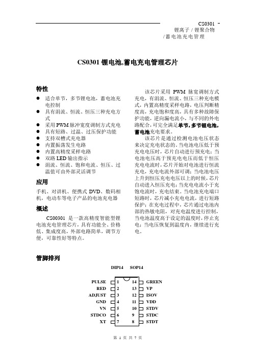
CS0301锂电池,蓄电充电管理芯片特性●适合单节,多节锂电池,蓄电池充电控制●具有涓流、恒流、恒压三种充电方式●采用PWM脉冲宽度调制方式充电●具有短路、过温、过压保护功能●支持双槽式充电器●内置振荡发生电路●内置高精度采样电路●双路LED输出指示●涓流、恒流、饱和电流、恒压、过温值可由外部灵活调节应用手机、对讲机、便携式DVD、数码相机,电动车等电子产品的电池充电器概述CS00301是一款高精度智能型锂电池充电管理芯片,具有功能全、价格低、集成度高,外部电路简单,调节方便,可靠性好等特点。
该芯片采用PWM脉宽调制方式充电,有涓流、恒流、恒压三种充电模式,内置高精度采样电路,电压判断精度高,充电饱和度高,具有多种故障保护功能,逆向漏电流小,与不同的外电路配合,可完全满足单节,多节锂电池,蓄电池充电要求。
该芯片是通过检测电池电压状态来决定充电状态的。
当电池电压低于预充电电压时,芯片自动进行预充电;当电池电压高于预充电电压而低于恒压充电电流时,芯片开始对电池进行恒流充电,充电电流外部可调;当电池电压上升到恒压充电电压以上的时候,芯片自动进入恒压充电;当充电电流小于充饱电流时,充电结束。
当电池充电端口短路时,芯片减小充电电流,进行短路保护;在充电过程中,芯片通过电池内部的热敏电阻,对充电温度进行控制,当电池温度高于设定的温度时,停止充电;当电压恢复到温度内,继续进行充电。
管脚排列极限参数电源电压V dd------ 3.0V ~ 7.0V输入口电压------ -0.5V ~ Vdd+0.5V结温------ 150℃工作温度------ -40 ~+85℃保存温度------ -65 ~+150℃注:超出所列的极限参数可能导致器件的永久性损坏。
以上给出的仅仅是极限范围,在这样的极限条件下工作,器件的技术指标将得不到保证,长期在这种条件下还会影响器件的可靠性。
电学参数功能框图典型应用电路典型应用电路工作参数管脚功能描述端,开漏输出。
开关型单节锂电池充电和升压放电控制芯片HB6266C

开关型单节锂电池充电和升压放电控制芯片HB6266C功能特性简述●适用于单节锂离子/锂聚合物高效率同步Buck充电器●电池反向放电高效同步Boost控制器●最大10V输入电源耐压●电池放电可低至3V●0.5%的充电电压控制精度● 1.5%的放电升压控制精度●ISET脚充电使能和电流设置●单键飞梭功能●Boost自动检测负载进入待机模式●待机模式总电流小于10uA●ILOAD脚放电电流待机阈值设置●恒压充电电压值可通过外接电阻微调●内置软启动●内置Boot-Strap二极管●峰值电流模补偿内置●开关频率750KHz●充电状态指示,电池电量指示●内置最大100mA电流LED驱动●电池短路检测,保护●内置过温关断●电池充电过压保护●电源输入限流DPM,过流保护●Cycle-by-cycle限流●Boost输出过流保护●外置充电时间设置●内置输入欠压过压保护●工作环境温度范围:-40℃~125℃●TSSOP-24或QFN-24封装应用●手持设备●PDVD,PDA和智能手机●电源管理概述HB6266为同步开关型高效锂离子/锂聚合物电池充电和升压放电控制芯片,非常适合于便携式设备的电源管理应用。
HB6266的充电集高精度电压和充电电流调节器、预充、充电状态指示和充电截止等功能于一体,而放电部分具有自动检测负载进入待机模式和电池电量过低报警功能。
HB6266对电池充电分为三个阶段:预充(Pre-charge)、恒流(CC/Constant Current)、恒压(CV/Constant Voltage)过程,恒流充电电流通过外部电阻决定,恒压充电电压可通过外部电阻微调。
HB6266内置输入电源限流环路,可根据负载情况动态调节电流分配,并具有快速响应和过流关断的功能。
HB6266集成的电池容量检测指示灯,无论在充电还是放电状态均可有效指示电池剩余电量。
HB6266内置LED手电筒驱动,由单键飞梭控制。
HB6266内置过温保护,充电时间限制,Cycle-by-cycle限流,Boost输出过流,过压及短路保护,确保芯片安全工作。
GS1407 单节锂电充电芯片
·最高输入可达 9V;
·自动再充电; ·2 个充电状态开漏输出引脚;
GS1407
·C/10 充电终止;
·待机模式下的供电电流为 40uA;
·2.9V涓流充电器件版本;
·软启动限制了浪涌电流; ·采用 6 引脚 SOT-23 封装。
400mA 电流完整的充电循环(600mAh)
绝对最大额定值
·输入电源电压(VCC):-0.3V~9V
V
mA mA mA μA μA μA mA V mV V mV V V mV mV mA mA V
I CHRG
CHRG 引脚漏电流
V =5V(待机模式) CHRG
0
1
μA
V CHRG
CHRG 引脚输出低电压
I CHRG
=5mA
0.3
0.6
V
3
TEL13509685286Q1839845898
引脚漏电流
反接后的 GS1407 当电池去除后,由于 GS1407 输出端 BAT 管脚电容电位仍为负值,
则GS1407指示灯不会立刻正常亮,只有正确 接入电池可自动激活充电。或者等待较长时间 BAT 端电容负电位的电量放光,BAT 端电位 大于零伏,GS1407 会显示正常的无电池指示 灯状态。
I
=5mA
STDBY
VFLOAT-VRECHRG
IBAT=0 至 IBAT=1000V/RPROG VBAT 高至低 IBAT 降至 ICHG/10 以下
GS1407
0
1
μA
0.3
0.6
V
100 150 200
mV
120
℃
650
mΩ
20
ms
FOSAN富信电子 IC DW01A-产品规格书
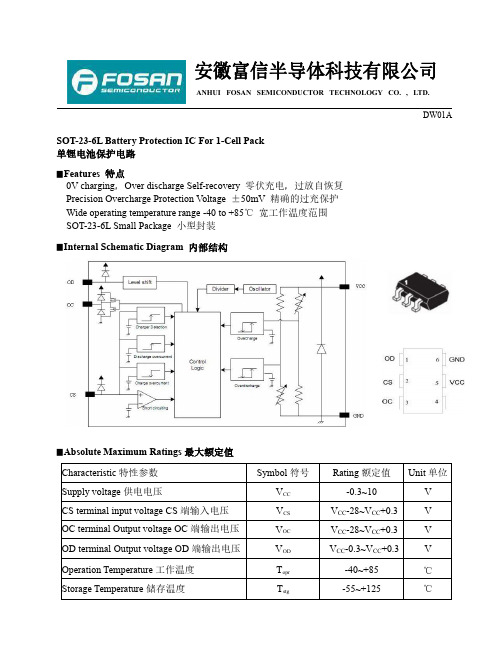
安徽富信半导体科技有限公司ANHUI FOSAN SEMICONDUCTOR TECHNOLOGY CO.,LTD.DW01A SOT-23-6L Battery Protection IC For1-Cell Pack单锂电池保护电路▉Features特点0V charging,Over discharge Self-recovery零伏充电,过放自恢复Precision Overcharge Protection Voltage±50mV精确的过充保护Wide operating temperature range-40to+85℃宽工作温度范围SOT-23-6L Small Package小型封装▉Internal Schematic Diagram内部结构▉Absolute Maximum Ratings最大额定值Characteristic特性参数Symbol符号Rating额定值Unit单位Supply voltage供电电压V CC-0.3~10V CS terminal input voltage CS端输入电压V CS V CC-28~V CC+0.3V OC terminal Output voltage OC端输出电压V OC V CC-28~V CC+0.3V OD terminal Output voltage OD端输出电压V OD V CC-0.3~V CC+0.3V Operation Temperature工作温度T opr-40~+85℃Storage Temperature储存温度T stg-55~+125℃安徽富信半导体科技有限公司ANHUI FOSAN SEMICONDUCTOR TECHNOLOGY CO.,LTD.DW01A ▉Electrical Characteristics电特性(T A=25℃unless otherwise noted如无特殊说明,温度为25℃)Characteristics特性参数(Test Condition测试条件)Symbol符号Min最小值Typ典型值Max最大值Unit单位Operating voltage between V CC&GND间工作电压V CC 1.5—9.0V Operating voltage between OC&CS间工作电压 1.5—25.0V Minimum operating voltage for0V charging零充电状态工作电压V st—— 1.2V Discharging overcurrent release resistance放电过流释放电阻(V CC=3.6V,V CS=1V)R short3050100KΩOC pin Nch ON voltage OC脚N沟道开启电压V CL—0.40.5V OC pin Pch ON voltage OC脚P沟道开启电压V CH V CC-0.1V CC-0.02—V OD pin Nch ON voltage OD脚N沟道开启电压V DL—0.20.5V OD pin Pch ON voltage OD脚P沟道开启电压V DH V CC-0.1V CC-0.02—V Current consumption消耗电流(V CC=3.5V,V CS=0V)I CC 1.2 2.4 6.0uA Overdischarge current consumption(Self-recovery)过放电(自恢复)消耗电流(V CC=V CS=2.0V)I DOX— 1.8 3.0uA Overcharge Protection Voltage过充保护电压(R1=100Ω)V OCP 4.25 4.30 4.35V Overcharge Release Voltage过充释放电压(R1=100Ω)V OCR 4.05 4.10 4.15V O v e r c h a r g e Hy s t e r e s i s V o lt a g e过充滞后电压(V hys=V OCP-V OCR,R1=100Ω)V hys—0.2—V Overdischarge Protection Voltage过放保护电压(V CS=0V,R1=100Ω)V ODP 2.30 2.40 2.50VOverdischarge Release Voltage(R1=100Ω)过放释放电压(R1=100Ω,R2=1KΩ,V CS=V chg)V ODR2.902.303.002.403.102.50VDischarging overcurrent detection voltage放电过流检测电压(V CC=3V,R2=1KΩ)V DO0.110.140.17V S ho r t C u rr e n t P r o t ec ti on V o lt a g e短路保护电压(V CC=3.0V)V short0.9 1.2 1.5V Overcharge Delay Time过充延时(V CC=3.8V→4.5V)T OC50100200msOverdischarge Delay Time过放延时(V CC=3.2V→2.2V)T OD50100200ms Discharging overcurrent delay time放电过流延时(V CC=3.0V,V CS=0→0.2V)T DO51020ms Short delay time短路延时(V CC=3.5V,V CS=0→1.0V)T short—50100sCharger detection voltage充电检测电压(V CC=3.6V,R2=1KΩ)Vchg0.30.7 1.1V安徽富信半导体科技有限公司ANHUI FOSAN SEMICONDUCTOR TECHNOLOGY CO.,LTD.DW01A▉ApplicationCircuit 应用电路No.脚号Name 名称Description 功能1OD Over-discharge protect control output 过放保护输出2CS Current detect input 电流检测输入3OC Over-charge protect control output 过充保护输出4NC 空5VCC Positive power Supply 正电源供电6GNDNegative power supply of battery side 电池侧负电源供电▉Dimension外形封裝尺寸SymbolDimensions In Millimeters Dimensions In InchesMinMaxMinMaxA 1.050 1.2500.0410.049A10.0000.1000.0000.004A2 1.050 1.1500.0410.045b 0.3000.5000.0120.020c 0.1000.2000.0040.008D 2.820 3.0200.1110.119E 1.500 1.7000.0590.067E1 2.650 2.9500.1040.116e 0.950TYP 0.037TYP e1 1.800 2.0000.0710.079L 0.600REF0.024REFθ0o8o0o8o。
如韵电子 可用太阳能电池供电的锂电池充电管理芯片 CN3063 说明书
(VIN=5V, 除非另外注明,TA=-40℃ 到 85℃, 典型值在环境温度为25℃时测得)
参数
符号
测试条件
最小 典型
最大
输入电源电压
VIN
4.35
6
工作电流 电源电压过低锁存阈
值
IVIN Vuvlo
BAT端无负载 VIN下降
400
650
950
3.7
3.9
电源电压过低检测阈
值迟滞
Huvlo
0.1
恒压充电电压 电池连接端电流 预充电阈值
。芯片内部的功率管理电路在芯片的结温超过115
℃时自动降低充电电流,这个功能可以使用户最大限度的利用芯片的功率处理能力,不用担心芯片过热
而损坏芯片或者外部元器件。这样,用户在设计充电电流时,可以不用考虑最坏情况,而只是根据典型
情况进行设计就可以了,因为在最坏情况下,CN3063会自动减小充电电流。
当输入电压大于低电压检测阈值和电池端电压时,CN3063开始对电池充电, 管脚输出低电平,表示
充电结束
在恒压充电状态,当施加在 CN3063 的第 4 管脚 VIN 的电压大于 4.45V,并且当充电电流小于所设置的 恒流充电电流的 1/10 时,充电周期结束。在输入电压源限流模式,即使充电电流小于所设置的恒流充电 电流的 1/10,充电也将继续,不会结束。这样可以保证即使在输入电压源的电流输出能力很微弱的情况 下,也能为电池充电。
而精确调制恒压充电时电池正极的电压,避免了从电池的正极到CN3063
的BAT管脚之间的导线电阻或接触电阻等寄生电阻对充电的影响。如果在
FB管脚和BAT管脚之间接一个电阻,可以调整恒压充电电压。
极限参数
管脚电压………………………-0.3V to 6.5V BAT 管脚短路持续时间………连续 存储温度…...……-65℃ to 150℃ 焊接温度(10 秒)……...…..300℃
- 1、下载文档前请自行甄别文档内容的完整性,平台不提供额外的编辑、内容补充、找答案等附加服务。
- 2、"仅部分预览"的文档,不可在线预览部分如存在完整性等问题,可反馈申请退款(可完整预览的文档不适用该条件!)。
- 3、如文档侵犯您的权益,请联系客服反馈,我们会尽快为您处理(人工客服工作时间:9:00-18:30)。
1
TEMP
2
PROG
VPROG *1100 RPROG
5
BAT
6
7
8
CE
V02
Page 2 of 18
TEL13509685286/29768716/Q1839845898
Block Diagram
GS1406
V02
Page 3 of 18
TEL13509685286/29768716/Q1839845898VBiblioteka 2Page 1 of 18
TEL13509685286/29768716/Q1839845898
Pin Configuration
GS1406
Pin Assignment
Pin Num. Symbol Function Temperature sense input Connecting TEMP pin to NTC thermistor’s output in Lithium ion battery pack. If TEMP pin’s voltage is below 45% or above 80% of supply voltage VCC, this means that battery’s temperature is too low or too high, charging is suspended. The temperature sense function can be disabled by grounding the TEMP pin. Constant Charge Current Setting and Charge Current Monitor Pin The charge current is programmed by connecting a resistor RPROG from this pin to GND. When in precharge mode, the PROG pin’s voltage is regulated to 0.1V. When charging in constant-current mode this pin’s voltage is regulated to 1V. In all modes during charging, the voltage on this pin can be used to measure the charge current using the following formula: IBAT = 3 4 GND VCC Ground Positive input supply voltage Provides power to the internal circuit. When VCC drops to within 80mV of the BAT pin voltage, the GS1406 enters low power sleep mode, dropping IBAT to less than 2μA. Battery connection Pin Connect the positive terminal of the battery to this pin. Dropping BAT pin ’s current to less than 2μA when IC in disable mode or in sleep mode. BAT pin provides charge current to the battery and provides regulation voltage of 4.2V. Charge terminated status output is pulled low by an internal switch to indicate a battery charge terminated; this means Charge termination. Otherwise pin is in high impedance state. Open-Drain charge status output When the battery is being charged, the pin is pulled low by an internal switch, otherwise, pin is in high impedance state. Chip enable input A high input will put the device in the normal operating mode. Pulling the CE pin to low level will put the GS1406 into disable mode. The CE pin can be driven by TTL or CMOS logic level.
TEL13509685286/29768716/Q1839845898
尚亿微电子 李华
GS1406
GS1406
1A Lithium Ion Battery Linear Charger
General Description
GS1406 is a complete constant-current/constant voltage
GS1406 is specifically designed to work within USB power
specifications. No external sense resistor is needed and no blocking diode is required due to the internal PMOSFET
Absolute Maximum Ratings
Parameter Input supply voltage : VCC PROG pin voltage BAT pin voltage TEMP pin voltage pin voltage pin voltage CE pin voltage BAT pin current PROG pin current Maximum junction temperature Operating ambient temperature :Topa Storage temperature :Tstr Soldering temperature and time Rating -0.3~8 -0.3~VCC+0.3 -0.3~7 -0.3~10 -0.3~10 -0.3~10 -0.3~10 1200 1200 145 -40~85 -65~125 +260(Recommended 10S) Unit V V V V V V V mA μA ℃ ℃ ℃ ℃
Features
●Protection of battery cell reverse connection ● Programmable charge current up to 1A ●No MOSFET sense resistor or blocking diode required ●Complete linear Charger in SOP8 Package for single Cell Lithium-Ion Batteries. ●Constant-Current/Constant-Voltage operation
th
state dropping the battery drain current to less than 2μA.The GS1406 can be put into shutdown mode reducing the supply current to 55μA. Other features include Battery temperature monitor, under-voltage lockout, automatic recharge and two status pins to indicate charge and charge termination.
GS1406
Caution: The absolute maximum ratings are rated values exceeding which the product could suffer physical damage. These values must therefore not be exceeded under any conditions.
Typical charge cycle(1000mAh battery)
Applications
●Cellular Telephones ●Digital Still Cameras ●MP3 Players ●Bluetooth Applications ●Portable Devices ●USB Bus-Powered Chargers
architecture .Thermal feedback regulates the charge current to limit the die temperature during high power operation or high ambient temperature .The charge voltage is fixed at 4.2V,and the charge current can be programmed externally with a single resistor. The GS1406 automatically terminates the charge cycle when the charge current drops to 1/10 the programmed value after the final float voltage is reached. When the input supply (wall adapter or USB supply) is removed the GS1406 automatically enters a low current