高压二极管HighVoltageRectifier
常用高压二极管简介及型号

二极管知识简介一、二极管的工作原理晶体二极管为一个由p型半导体和n型半导体形成的p-n结,在其界面处两侧形成空间电荷层,并建有自建电场。
当不存在外加电压时,由于p-n 结两边载流子浓度差引起的扩散电流和自建电场引起的漂移电流相等而处于电平衡状态。
当外界有正向电压偏置时,外界电场和自建电场的互相抑消作用使载流子的扩散电流增加引起了正向电流。
当外界有反向电压偏置时,外界电场和自建电场进一步加强,形成在一定反向电压范围内与反向偏置电压值无关的反向饱和电流I0。
当外加的反向电压高到一定程度时,p-n结空间电荷层中的电场强度达到临界值产生载流子的倍增过程,产生大量电子空穴对,产生了数值很大的反向击穿电流,称为二极管的击穿现象。
二、二极管的类型二极管种类有很多,按照所用的半导体材料,可分为锗二极管(Ge管)和硅二极管(Si管)。
根据其不同用途,可分为检波二极管、整流二极管、稳压二极管、开关二极管等。
按照管芯结构,又可分为点接触型二极管、面接触型二极管及平面型二极管。
点接触型二极管是用一根很细的金属丝压在光洁的半导体晶片表面,通以脉冲电流,使触丝一端与晶片牢固地烧结在一起,形成一个“PN结”。
由于是点接触,只允许通过较小的电流(不超过几十毫安),适用于高频小电流电路,如收音机的检波等。
面接触型二极管的“PN结”面积较大,允许通过较大的电流(几安到几十安),主要用于把交流电变换成直流电的“整流”电路中。
平面型二极管是一种特制的硅二极管,它不仅能通过较大的电流,而且性能稳定可靠,多用于开关、脉冲及高频电路中。
三、二极管的导电特性二极管最重要的特性就是单方向导电性。
在电路中,电流只能从二极管的正极流入,负极流出。
下面通过简单的实验说明二极管的正向特性和反向特性。
1.正向特性在电子电路中,将二极管的正极接在高电位端,负极接在低电位端,二极管就会导通,这种连接方式,称为正向偏置。
必须说明,当加在二极管两端的正向电压很小时,二极管仍然不能导通,流过二极管的正向电流十分微弱。
肖特基二极管讲解

肖特基二极管简介肖特基二极管(SBD)是肖特基势垒二极管(SchottkyBarrierDiode,缩写成SBD)的简称,是以其发明人肖特基博士(Schottky)命名的半导体器件。
肖特基二极管是低功耗、大电流、超高速半导体器件,它不是利用P型半导体与N型半导体接触形成PN结原理制作的,而是利用金属与半导体接触形成的金属-半导体结原理制作的。
因此,SBD也称为金属-半导体(接触)二极管或表面势垒二极管,它是一种热载流子二极管。
Schottky diode (SBD) is the Schottky barrier diode , is the inventor of the Schottky named semiconductor device. Schottky barrier diode is a low power, high current, super high speed semiconductor devices, instead of using P type semiconductor and the n-type semiconductor contact formation PN junction theory to make, but the use of metal semiconductor contact formation of metal semiconductor junction with the principle of making the. Therefore, SBD is also known as a metal semiconductor (contact) diode or a surface barrier diode, which is a hot carrier diode.肖特基二极管是半导体器件,以其发明人博士(1886年7月23日—1976年3月4日)命名的,SBD是肖特基势垒二极管(SchottkyBarrierDiode,缩写成SBD)的简称。
ru3yx二极管参数代换
ru3yx二极管参数代换英文回答:The ru3yx diode is a high-voltage, high-currentrectifier diode that is commonly used in power supplies and other electronic circuits. It has a reverse voltage rating of 300V and a forward current rating of 1A. The diode is also characterized by its low forward voltage drop of 0.7V and its fast switching speed.The ru3yx diode is a suitable replacement for a variety of other rectifier diodes, including the 1N4007, 1N5408, and UF4007 diodes. These diodes have similar voltage and current ratings to the ru3yx diode, and they also have low forward voltage drops and fast switching speeds.When replacing a ru3yx diode with another diode, it is important to consider the following factors:The reverse voltage rating of the replacement diodemust be equal to or greater than the reverse voltage rating of the ru3yx diode.The forward current rating of the replacement diode must be equal to or greater than the forward current rating of the ru3yx diode.The forward voltage drop of the replacement diode should be as close as possible to the forward voltage drop of the ru3yx diode.The switching speed of the replacement diode should be as fast as or faster than the switching speed of the ru3yx diode.By considering these factors, you can ensure that the replacement diode will function properly in place of theru3yx diode.中文回答:ru3yx二极管是一款高压大电流整流二极管,常用于电源及其他电子电路中。
二极管参数-HY+ELECTRONIC+CORP

●Guard ●Low
power loss,high efficiency current capability,low VF surge capacity package has UL flammability classification
●High ●High
1.0(25.4) MIN.
.052(1.3) DIA .048(1.2)
Dimensions in inches and (millimeters)
MAXIMUM RATINGS AND ELECTRICAL CHARACTERISTICS
Rating at 25℃ ambient temperature unless otherwise specified. Single phase, half wave ,60Hz, resistive or inductive load. For capacitive load, derate current by 20%
10SQ030 thru 10SQ100
SCHOTTKY BARRIER RECTIFIERS REVERSE VOLTAGE -30 to 100Volts FORWARD CURRENT -10.0 Amperes R-6
FEATURES
●Metal
of silicon rectifier , majority carrier conduction ring for transient protection
1000
TJ=25℃ ,f=1MHZ 100 0.1 1 4 10 100
REVERSE VOLTAGE VOLTS
UNIT V V V A
IFSM VF IR 0.55
西门子肖特基二极管 MBR1100-D 使用手册说明书
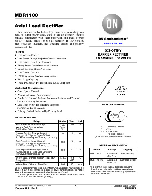
MBR1100Axial Lead RectifierThese rectifiers employ the Schottky Barrier principle in a large area metal−to−silicon power diode. State−of−the−art geometry features epitaxial construction with oxide passivation and metal overlap contact. Ideally suited for use as rectifiers in low−voltage, high−frequency inverters, free wheeling diodes, and polarity protection diodes.Features•Low Reverse Current•Low Stored Charge, Majority Carrier Conduction•Low Power Loss/High Efficiency•Highly Stable Oxide Passivated Junction•Guard−Ring for Stress Protection•Low Forward V oltage•175°C Operating Junction Temperature•High Surge Capacity•These Devices are Pb−Free and are RoHS CompliantMechanical Characteristics:•Case: Epoxy, Molded•Weight: 0.4 Gram (Approximately)•Finish: All External Surfaces Corrosion Resistant and Terminal Leads are Readily Solderable•Lead Temperature for Soldering Purposes:260°C Max. for 10 Seconds•Polarity: Cathode Indicated by Polarity BandMAXIMUM RATINGSRating Symbol Value UnitPeak Repetitive Reverse Voltage Working Peak Reverse Voltage DC Blocking Voltage V RRMV RWMV R100VAverage Rectified Forward Current (V R(equiv)≤0.2 V R(dc), R q JA = 50°C/W,P.C. Board Mounting, [see Note 3], T A = 120°C)I O 1.0APeak Repetitive Forward Current(V R(equiv)≤ 0.2 V R(dc), R q JA = 50°C/W,P.C. Board Mounting, [see Note 3], T A = 110°C)I FRM2.0ANon−Repetitive Peak Surge Current (Surge Applied at Rated Load Conditions Halfwave, Single Phase, 60 Hz)I FSM50AOperating and Storage Junction Temperature Range (Note 1)T J, T stg−65 to+175°CVoltage Rate of Change (Rated V R)dv/dt10V/ns Stresses exceeding those listed in the Maximum Ratings table may damage the device. If any of these limits are exceeded, device functionality should not be assumed, damage may occur and reliability may be affected.1.The heat generated must be less than the thermal conductivity fromJunction−to−Ambient: dP D/dT J < 1/R q JA.Device Package Shipping†ORDERING INFORMATIONSCHOTTKYBARRIER RECTIFIER1.0 AMPERE, 100 VOLTSMBR1100G Axial Lead(Pb−Free)1000 Units/Bag†For information on tape and reel specifications, including part orientation and tape sizes, please refer to our Tape and Reel Packaging Specification Brochure, BRD8011/D.MBR1100RLG Axial Lead(Pb−Free)5000/T ape & ReelMARKING DIAGRAMA= Assembly LocationY= YearWW= Work WeekG= Pb−Free Package(Note: Microdot may be in either location)THERMAL CHARACTERISTICS (See Note 4)CharacteristicSymbol Max Unit Thermal Resistance, Junction−to−AmbientR q JASee Note 3°C/WELECTRICAL CHARACTERISTICS (T L = 25°C unless otherwise noted)CharacteristicSymbol MaxUnit Maximum Instantaneous Forward Voltage (Note 2)(i F = 1 A, T L = 25°C)(i F = 1 A, T L = 100°C)V F0.790.69VMaximum Instantaneous Reverse Current @ Rated dc Voltage (Note 2)(T L = 25°C)(T L = 100°C)i R0.55.0mA2.Pulse Test: Pulse Width = 300 m s, Duty Cycle ≤2.0%.Figure 1. Typical Forward Voltage Figure 2. Typical Reverse Current {Figure 3. Current Derating (Mounting Method 3 per Note 3)Figure 4. Power Dissipation0.60.90v F , INSTANTANEOUS VOLTAGE (VOLTS)20102.05.01.0V R , REVERSE VOLTAGE (VOLTS)609000.20.040.020.011201600T A , AMBIENT TEMPERATURE (°C)4.03.02.01.0I F(AV), AVERAGE FORWARD CURRENT (AMPS)1.004.03.02.01.02.0140i F , I N S T A N T A N E O U S F O R W A R D C U R R E N T (A M P S )I I P F (A V ), A V E R A G E P O W E R D I S S I P A T I O N (W A T T S )0.50.20.10.30.10.20.40.50.70.8708010203040500.10.41.020********* 3.0 4.0 5.00.050.021.1 1.41.0 1.2 1.3100, R E V E R S E C U R R E N T ( A )R m 4.02.01020100402001 K400200180, A V E R A G E F O R W A R D C UR R E N T (A M P S )F (A V){ The curves shown are typical for the highest voltage device in the voltage grouping. Typical reverse current for lower voltage selections can be estimated from these same curves if V R is sufficiently below rated V R .Figure 5. Typical Capacitance2040V R , REVERSE VOLTAGE (VOLTS)150504*********C , C A P A C I T A N C E (p F )50100601001070809070609080NOTE 3 — MOUNTING DATA:Data shown for thermal resistance junction−to−ambient (R q JA) for the mounting shown is to be used as a typical guideline values for preliminary engineering or in case the tie point temperature cannot be measured.Typical Values for R q JA in Still AirMounting MethodLead Length, L (in)R q JA 1/81/41/23/4152657285°C/W 2678087100°C/W 3—50°C/WMounting Method 1P .C. Board with 1−1/2″ x 1−1/2″copper surface.Mounting Method 3P .C. Board with1−1/2″ x 1−1/2″copper surface.PLANEMounting Method 2″NOTE 4 — THERMAL CIRCUIT MODEL:(For heat conduction through the leads)Use of the above model permits junction to lead thermal resistance for any mounting configuration to be found. For a given total lead length, lowest values occur when one side of the rectifier is brought as close as possible to the heat sink.Terms in the model signify:T A = Ambient Temperature T C = Case Temperature T L = Lead Temperature T J = Junction Temperature R q S = Thermal Resistance, Heat Sink to Ambient R q L = Thermal Resistance, Lead to Heat Sink R q J = Thermal Resistance, Junction to Case P D = Power Dissipation(Subscripts A and K refer to anode and cathode sides,respectively.) V alues for thermal resistance components are:R q L = 100°C/W/in typically and 120°C/W/in maximum.R q J = 36°C/W typically and 46°C/W maximum.NOTE 5 — HIGH FREQUENCY OPERATION:Since current flow in a Schottky rectifier is the result of majority carrier conduction, it is not subject to junction diode forward and reverse recovery transients due to minority carrier injection and stored charge. Satisfactory circuit analysis work may be performed by using a model consisting of an ideal diode in parallel with a variable capacitance. (See Figure 5)Rectification efficiency measurements show that operation will be satisfactory up to several megahertz. For example, relative waveform rectification efficiency is approximately 70 percent at 2 MHz, e.g., the ratio of dc power to RMS power in the load is 0.28 at this frequency,whereas perfect rectification would yield 0.406 for sine wave inputs. However, in contrast to ordinary junction diodes, the loss in waveform efficiency is not indicative of power loss: it is simply a result of reverse current flow through the diode capacitance, which lowers the dc output voltage.SCALE 1:1BDIM MIN MAX MIN MAX MILLIMETERSINCHES A 4.10 5.200.1610.205B 2.00 2.700.0790.106D 0.710.860.0280.034F −−− 1.27−−−0.050K25.40−−−1.000−−−NOTES:1.DIMENSIONING AND TOLERANCING PER ANSI Y14.5M, 1982.2.CONTROLLING DIMENSION: INCH.3.ALL RULES AND NOTES ASSOCIATED WITH JEDEC DO −41 OUTLINE SHALL APPLY4.POLARITY DENOTED BY CATHODE BAND.5.LEAD DIAMETER NOT CONTROLLED WITHIN F DIMENSION.AXIAL LEAD CASE 59−10ISSUE UDATE 15 FEB 2005GENERICMARKING DIAGRAM*xxx = Specific Device Code A = Assembly Location YY = YearWW= Work WeekSTYLE 1:PIN 1.CATHODE (POLARITY BAND)2.ANODESTYLE 2:NO POLARITYSTYLE 1STYLE 2*This information is generic. Please refer to device data sheet for actual part marking.Pb −Free indicator, “G” or microdot “ G ”,may or may not be present.MECHANICAL CASE OUTLINEPACKAGE DIMENSIONSON Semiconductor and are trademarks of Semiconductor Components Industries, LLC dba ON Semiconductor or its subsidiaries in the United States and/or other countries.ON Semiconductor reserves the right to make changes without further notice to any products herein. ON Semiconductor makes no warranty, representation or guarantee regarding the suitability of its products for any particular purpose, nor does ON Semiconductor assume any liability arising out of the application or use of any product or circuit, and specifically disclaims any and all liability, including without limitation special, consequential or incidental damages. ON Semiconductor does not convey any license under its patent rights nor thePUBLICATION ORDERING INFORMATIONTECHNICAL SUPPORTNorth American Technical Support:Voice Mail: 1 800−282−9855 Toll Free USA/Canada Phone: 011 421 33 790 2910LITERATURE FULFILLMENT :Email Requests to:*******************onsemi Website: Europe, Middle East and Africa Technical Support:Phone: 00421 33 790 2910For additional information, please contact your local Sales Representative。
高效整流二极管HER302
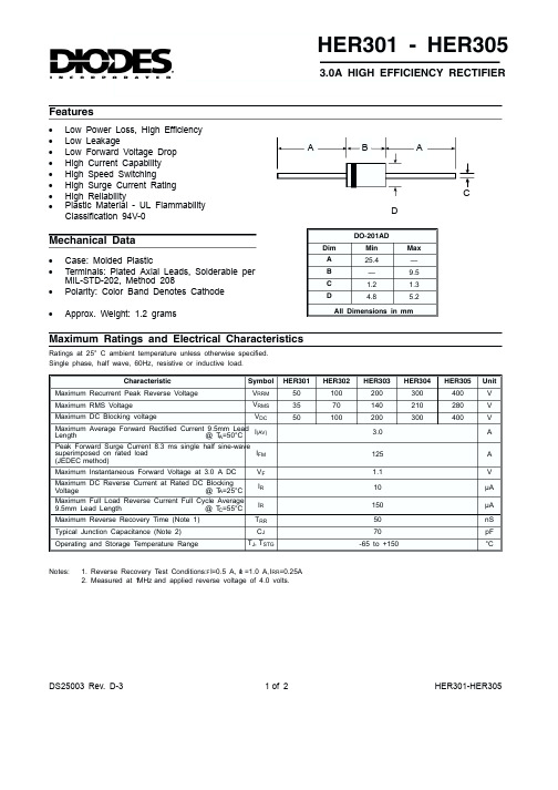
D S 25003 Rev. D-3 1 of 2 HER301-HER305FeaturesMechanical Data·Case: Molded Plastic·Terminals: Plated Axial Leads, Solderable per MIL-STD-202, Method 208·Polarity: Color Band Denotes Cathode ·Approx. Weight: 1.2 gramsRatings at 25° C ambient temperature unless otherwise specified.Single phase, half wave, 60Hz, resistive or inductive load.Maximum Ratings and Electrical CharacteristicsCharacteristicSymbol HER301HER302HER303HER304HER305Unit Maximum Recurrent Peak Reverse Voltage V RRM 50100200300400V Maximum RMS Voltage V RMS 3570140210280V Maximum DC Blocking voltageV DC50100200300400V Maximum Average Forward Rectified Current 9.5mm Lead Length @ T A =50°C I(AV)3.0A Peak Forward Surge Current 8.3 ms single half sine-wavesuperimposed on rated load(JEDEC method)I FM 125A Maximum Instantaneous Forward Voltage at 3.0 A DC V F 1.1V Maximum DC Reverse Current at Rated DC Blocking Voltage @ TA=25°C I R 10µA Maximum Full Load Reverse Current Full Cycle Average 9.5mm Lead Length @ T C =55°C I R 150µA Maximum Reverse Recovery Time (Note 1)T RR 50nS Typical Junction Capacitance (Note 2)C J 70pF Operating and Storage Temperature RangeT J ,T STG-65 to +150°CNotes:1. Reverse Recovery Test Conditions: I F =0.5 A, I R =1.0 A,I RR =0.25A2. Measured at 1MHz and applied reverse voltage of 4.0 volts.·Low Power Loss, High Efficiency ·Low Leakage·Low Forward Voltage Drop ·High Current Capability ·High Speed Switching·High Surge Current Rating ·High Reliability·Plastic Material - UL Flammability Classification 94V-0AAB CDHER301 - HER3053.0A HIGH EFFICIENCY RECTIFIERDO-201ADDim Min Max A 25.4—B —9.5C 1.2 1.3D4.85.2All Dimensions in mmD S 25003 Rev. D-3 2 of 2 HER301-HER3051001751101001000NUMBER OF CYCLES A T 60HzFig.4,Max.Non-Repetitive Peak ForwardSurge Current00255075100125150175T ,AMBIENT TEMPERATURE (°C)Fig.1,Typical Forward Current Derating Curve A Single Phase Half Wave 60Hz Resistive or Inductive Load0.51.01.52.02.53.002550751001251501750.11.0101001000V ,REVERSE VOLTAGE (VOLTS)Fig.5,Typical JunctionCapacitanceR 0.010.11.01010000.20.40.60.8 1.0 1.2 1.4V ,INSTANTANEOUS FWD VOLTAGE (V)Fig.3,Typ.Instantaneous Forward CharacteristicsF T =25°CJ 0.010.11.0101001000020406080100120140PERCENT OF RATED PEAK REVERSE VOLTAGEFig.2,Typical Reverse CharacteristicsT =150°CJ T =100°CJ T =25°CJ。
R5000, 高压二极管中文资料

IFSM
30
A
VFM IRM Cj RqJA Tj, TSTG
5.0 5.0 15 50 -65 to +125
V mA pF K/W °C
Notes:
1. Valid provided that leads are kept at ambient temperature at a distance of 9.5mm from the case. 2. Measured at 1.0MHz and applied reverse voltage of 4.0V DC.
Characteristic Peak Repetitive Reverse Voltage Working Peak Reverse Voltage DC Blocking Voltage RMS Reverse Voltage Average Rectified Output Current (Note 1) @ TL = 55
D
DO-15 Dim A B C D Min 25.40 5.50 0.686 2.60 All Dimensions in mm Max — 7.62 0.889 3.60
A
B
A
Mechanical Data
! ! ! ! ! ! !
C
Case: DO-15,Molded Plastic Terminals: Plated Leads Solderable per MIL-STD-202, Method 208 Polarity: Cathode Band Weight: 0.40 grams (approx.) Mounting Position: Any Marking: Type Number
肖特基二极管
肖特基二极管简介肖特基二极管(SBD)是肖特基势垒二极管(SchottkyBarrierDiode,缩写成SBD)的简称,是以其发明人肖特基博士(Schottky)命名的半导体器件。
肖特基二极管是低功耗、大电流、超高速半导体器件,它不是利用P型半导体与N型半导体接触形成PN结原理制作的,而是利用金属与半导体接触形成的金属-半导体结原理制作的。
因此,SBD也称为金属-半导体(接触)二极管或表面势垒二极管,它是一种热载流子二极管。
Schottky diode (SBD) is the Schottky barrier diode , is the inventor of the Schottky named semiconductor device. Schottky barrier diode is a low power, high current, super high speed semiconductor devices, instead of using P type semiconductor and the n-type semiconductor contact formation PN junction theory to make, but the use of metal semiconductor contact formation of metal semiconductor junction with the principle of making the. Therefore, SBD is also known as a metal semiconductor (contact) diode or a surface barrier diode, which is a hot carrier diode.肖特基二极管是半导体器件,以其发明人博士(1886年7月23日—1976年3月4日)命名的,SBD是肖特基势垒二极管(SchottkyBarrierDiode,缩写成SBD)的简称。
- 1、下载文档前请自行甄别文档内容的完整性,平台不提供额外的编辑、内容补充、找答案等附加服务。
- 2、"仅部分预览"的文档,不可在线预览部分如存在完整性等问题,可反馈申请退款(可完整预览的文档不适用该条件!)。
- 3、如文档侵犯您的权益,请联系客服反馈,我们会尽快为您处理(人工客服工作时间:9:00-18:30)。
R4000
40004000280045
300.25.0R4000
5.0
30
R4000
反向电压 4000V 正向电流 0.2 A
V
μA
pF
I R
Cj
最大正向电压 I F =0.2A
最大反向电流 TA= 25℃典型结电容 V R = 4.0V, f = 1MHz 电特性 TA = 25℃ 除非另有规定。
Electrical Characteristics Ratings at 25℃ ambient temperature unless otherwise specified.
单位
Unit
符号
Symbols
Maximum forward voltage
Maximum reverse current Type junction capacitance
V F
-55--- +150V V V A A ℃/W
℃
V RRM V RMS V DC I F(AV)I FSM 特征 Features
·反向漏电流低 Low reverse leakage
·正向浪涌承受能力较强 High forward surge capability
·高温焊接保证 High temperature soldering guaranteed:
260℃/10 秒, 0.375" (9.5mm)引线长度。
260℃/10 seconds, 0.375" (9.5mm) lead length,·引线可承受5 磅 (2.3kg) 拉力。
5 lbs. (2.3kg) tension 机械数据 Mechanical Data
·端子: 镀锡轴向引线 Terminals: Plated axial leads
·极性: 色环端为负极 Polarity: Color band denotes cathode end ·安装位置: 任意 Mounting Position: Any
极限值和温度特性 TA = 25℃ 除非另有规定。
Maximum Ratings & Thermal Characteristics Ratings at 25℃ ambient temperature unless otherwise specified.
最大可重复峰值反向电压
Maximum repetitive peak reverse voltage 最大均方根电压 Maximum RMS voltage 最大直流阻断电压
Maximum DC blocking voltage
最大正向平均整流电流
Maximum average forward rectified current 峰值正向浪涌电流 8.3ms单一正弦半波
Peak forward surge current 8.3 ms single half sine-wave
典型热阻 Typical thermal resistance
工作结温和存储温度
符号
Symbols
单位
Unit
Reverse Voltage 4000V Forward Current 0.2 A
Operating junction and storage temperature range
Tj, TSTG R θj-a
高压二极管
High Voltage Rectifier
TA= 100℃50
·引线和管体皆符合RoHS标准 。
Lead and body according with RoHS standard
0255075100125150175
0.01
0.1
1
10
4.8
5.2 5.6
1
2
4610
20
40
100
40
30
20
10
0T j = 25°C
R4000
正向电流 I F (A )
正向特性曲线(典型值)
正向电压 V F (V)
环境温度 Ta(°C )
通过电流的周期
峰值正向浪涌电流 I F S M (A )
平均正向电流 I F (A V ) (A )浪涌特性曲线(最大值)特性曲线 Characteristic Curves
TYPICAL FORWARD CHARACTERISTIC
FORWARD CURRENT DERATING CURVE
I F I n s t a n t a n e o u s F o r w a r d C u r r e n t (A )
V F Instantaneous Forward Voltage (V)Tamb, ambient temperature (°C)
I F (A ) A v e r a g e F o r w a r d R e c t i f i e d C u r r e n t (A )
MAXIMUM NON REPETITIVE PEAK FORWARD SURGE CURRENT
Number of Cycles at 60 Hz.
I F S M P e a k F o r w a r d S u r g e C u r r e n t (A )
正向电流降额曲线
4.0 4.4。