CST仿真FSS详细步骤
电磁仿真CST入门教程
电磁仿真CST⼊门教程1.1 软件介绍CST公司总部位于德国达姆施塔特市,成⽴于1992年。
它是⼀家专业电磁场仿真软件的提供商。
CST软件采⽤有限积分法(Finite Integration)。
其主要软件产品有:CST微波⼯作室——三维⽆源⾼频电磁场仿真软件包(S参量和天线)CST设计⼯作室——微波⽹络(有源及⽆源)仿真软件平台(微波放⼤器、混频器、谐波分析等)CST电磁⼯作室——三维静场及慢变场仿真软件包(电磁铁、变压器、交流接触器等)马飞亚(MAFIA)——通⽤⼤型全频段、⼆维及三维电磁场仿真软件包(包含静电场、准静场、简谐场、本振场、瞬态场、带电粒⼦与电磁场的⾃恰相互作⽤、热动⼒学场等模块)在此,我们主要讨论“CST微波⼯作室”,它是⼀款⽆源微波器件及天线仿真软件,可以仿真耦合器、滤波器、环流器、隔离器、谐振腔、平⾯结构、连接器、电磁兼容、IC封装及各类天线和天线阵列,能够给出S参量、天线⽅向图等结果。
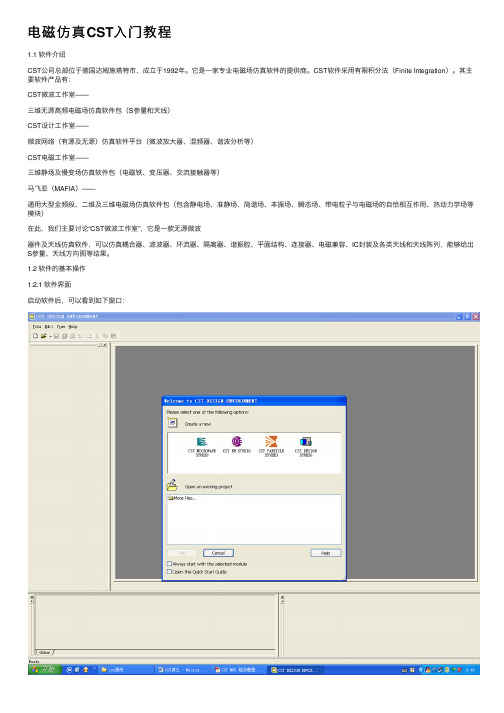
1.2 软件的基本操作1.2.1 软件界⾯启动软件后,可以看到如下窗⼝:1.2.2 ⽤户界⾯介绍1.2.3 基本操作1).模板的选择CST MWS内建了数种模板,每种模板对特定的器件类型都定义了合适的参数,选⽤适合⾃⼰情况的模板,可以节省设置时间提⾼效率,对新⼿特别适⽤,所有设置在仿真过程中随时都可以进⾏修改,熟练者亦可不使⽤模板模板选取⽅式:1,创建新项⽬ File—newFile—select template2,随时选⽤模板2)设置⼯作平⾯⾸先设置⼯作平⾯(E dit-working Plane Properties )将捕捉间距改为 1以下步骤可遵循仿真向导(Help->QuickStart Guide )依次进⾏1)设置单位(Solve->Units )合适的单位可以减少数据输⼊的⼯作量模板参数模板类型2)能够创建的基本模型3)改变视⾓快捷键为:视觉效果的改变:4)⼏何变换四种变换:5)图形的布尔操作四种布尔操作:例如:这⾥以“减”来说明具体操作1,两种不同材料的物体 2,选择第⼀个物体(⽴⽅体)3点击⼯具栏上的图标或在主菜单选择Objects->Boolean->Subtract4,选择第⼆个物体(圆球)5,回车确定6)选取模型的点、边、⾯对每种“选取操作”,都必须选择相应的选取⼯具。
3_CST软件在频率选择表面仿真中的应用

【CST软件在频率选择表面仿真中的应用】采用的模块为CST MWS-T和MWS-F。
前者主要用于非周期性的FSS结构,而后者则是用于周期性FSS结构,效率和精度均很高。
在实际隐身应用时,FSS均无法做成二维平面无穷周期的,所以在仿真实际载体的FSS特性时,必须采用MWS-T来进行。
所以这两类算法具有良好的互补关系,进而也覆盖了FSS的全部仿真应用。
1、双层Y型FSS采用CST MWS-F频域有限元法和Unit-Cell(元胞)边界条件,只需对一个FSS周期进行仿真,便可快速精确地得到其在不同入射角下的传输特性。
对于双层Y型FSS,两层FSS结构嵌在五层介质之间,可以在较宽的频率范围内进行选择性传输。
垂直入射时的传输特性FSS金属片上的表面电流10GHz下电场分布,可见被阻断(阻带)15GHz下电场分布,可见能够通过FSS(通带)2、特殊FSS结构-- 左手材料,又称超材料Meta-material,其实质也是一种FSS结构Split Ring Resonator(SRR)阵列置于共面波导(CPW)介质片的背面结构上,在每个SRR的圆心处,背面的金属线与两边金属线短路。
CST MWS频域有限元求解器在Unit Cell 边界条件下得出下右图所示的带通特性。
在通带外,有很强的衰减。
3、有限周期的双谐振环采用CST MWS时域求解器对下面这样一个有限周期双谐振环的三维结构进行了仿真。
在一定的频段上此结构呈现正折射率时入射波的传输方向见下面中图所示,右下图则给出了在另一个频段上结构呈现负折射率时相同的入射波却呈现了不同的传输方向。
这也能够达到隐身的目的,即折射了入射雷达波朝着一个非正常视角方向。
4、负属性材料所谓负属性表示,介电常数和/或磁导率可能是小于零的值。
自然界上实际上并不存在负属性材料,但通过某种材料结构的组合,可以在宏观上对外呈现视在的负属性现象。
如右图以及下面三图所示的电磁波的传播情况,就是采用CST MWS时域求解器仿真的有三层不同属性材料所组成的结构。
简述利用cst软件进行模拟仿真的大致流程。
简述利用cst软件进行模拟仿真的大致流程。
《利用CST软件进行模拟仿真的流程详解》一、引言在现代科技发展的大潮中,仿真软件的使用已经成为了电磁学和射频领域中不可或缺的一部分。
特别是CST Studio Suite作为其中的佼佼者,其在电磁仿真领域有着不可撼动的地位。
本文将对利用CST软件进行模拟仿真的大致流程进行详细的介绍和解析,帮助读者更好地了解和掌握其工作原理和操作方法。
二、CST软件的基本概述CST Studio Suite是一款专业的电磁仿真软件,主要面向射频、微波和毫米波等领域的工程师和科研人员。
其具有强大的建模能力和精准的仿真结果,被广泛应用于天线设计、射频集成电路、电磁兼容性和电磁干扰等领域。
三、利用CST软件进行模拟仿真的大致流程1. 问题定义与建模在利用CST软件进行模拟仿真之前,首先需要对待解决的问题进行准确定义,并进行合适的建模。
在问题定义阶段,需清晰地列出所需要解决的电磁学问题,如天线的设计、射频系统的性能分析等。
建模阶段则需要利用CST软件提供的建模工具进行准确的几何建模,以及对材料属性和边界条件进行设定。
2. 网格划分与求解设置建模完成后,需要对模型进行网格划分,以及对求解器进行合适的设置。
网格划分需要根据几何形状和电磁波长进行调整,以保证仿真结果的准确性。
在求解设置阶段,一般需要设定频率、激励方式、边界条件等参数,以便进行仿真求解。
3. 仿真求解与结果分析进行仿真求解后,需要对求解结果进行详细的分析。
利用CST软件提供的后处理工具,可以对电场分布、磁场分布、S参数等结果进行可视化和分析,以获取对电磁问题的深入理解。
还可以通过对比实验结果和仿真结果,对模型进行修正和优化。
四、个人观点和理解CST Studio Suite作为电磁仿真领域的佼佼者,其在建模和求解的能力上有着无可比拟的优势。
通过对模拟仿真流程的了解和掌握,可以更好地应用CST软件进行电磁学问题的求解和分析,为电磁学领域的研究和实践提供强有力的支持。
cst射频干扰仿真的工作流程

cst射频干扰仿真的工作流程下载温馨提示:该文档是我店铺精心编制而成,希望大家下载以后,能够帮助大家解决实际的问题。
文档下载后可定制随意修改,请根据实际需要进行相应的调整和使用,谢谢!并且,本店铺为大家提供各种各样类型的实用资料,如教育随笔、日记赏析、句子摘抄、古诗大全、经典美文、话题作文、工作总结、词语解析、文案摘录、其他资料等等,如想了解不同资料格式和写法,敬请关注!Download tips: This document is carefully compiled by theeditor.I hope that after you download them,they can help yousolve practical problems. The document can be customized andmodified after downloading,please adjust and use it according toactual needs, thank you!In addition, our shop provides you with various types ofpractical materials,such as educational essays, diaryappreciation,sentence excerpts,ancient poems,classic articles,topic composition,work summary,word parsing,copy excerpts,other materials and so on,want to know different data formats andwriting methods,please pay attention!CST(Computer Simulation Technology)射频干扰仿真的工作流程通常涉及多个细致的步骤,以确保仿真结果的准确性和实用性。
FSS-CST CST散射仿真
FSS: Simulation of Resonator ArrayTutorialsA BSTRACTA Frequency Selective Surface (FSS) is a periodic assembly of one- or two-dimensional resonant structures, either asapertures in a thin conducting sheet or as metallic patches on a substrate, which may have a band-pass or band-stop function respectively. The increasing interest within the high-frequency community in this sort of structure has also made its accurate simulation increasingly important. This tutorial describes how a FSS structure may be simulated efficiently using CST MICROWAVE STUDIO® (CST MWS). A simple unit cell of a ring resonator band-stop infinite array is considered as an example.ContentsIntroductionPhysical descriptionCST MICROWAVE STUDIO® ModelSimulation resultsParameter sweep analysisConclusionIntroductionPhysical descriptionFrequency selective surfaces are increasingly used for the frequency filtering of plane waves in radar or communications systems. A one- or two-dimensional periodic array of resonant structures on a backing material, either apertures in a metallic sheet or metallic patches on a substrate, acts as a filter for a plane wave arriving from any angle of incidence. In this example an array of full wavelength resonant conducting rings on a dielectric substrate is simulated. Since the FSS would be used on curved structures like radomes, it is desirable that the FSS have the same resonant frequency for all incident plane wave angles. For a given polarisation, ring resonators are known to be stable with the scan angle. CST MICROWAVE STUDIO® (CST MWS) can be used to establish the angular dependence of the resonant frequency.CST MICROWAVE STUDIO® Model: Parameter definition and preliminary settingsThe simulation of an entire array of resonant rings would be prohibitively time and memory consuming. The use of CST MWS’s unit cell boundary conditions in the directions of periodicity allows a rapid but no less accurate simulation of large surfaces. Setting up the simulation may be greatly eased by using the “FSS – Unit Cell (FD)” template, which automatically applies unit cell boundary conditions in the x- and y-directions and sets up Floquet port excitations in the positive and negative z-directions. There is no need to define master and slave boundary conditions; the phase relation of the opposing boundaries is automatically set by specifying the incident angle of the inward travelling plane wave.It is only necessary to construct a single ring on its backing substrate. Construction of the geometry itself is simple: a substrate is defined using a brick primitive object, and then a hollow cylinder can be used to create the ring. The conducting ring is a “lossy metal” type copper, and the substrate is Arlon AD 300 with a relative permittivity of 3.Figure 1 - The “FSS - Unit Cell (FD)” template simplifies simulation set-up by automatically setting the unit cell boundaryconditions.The incident angle of the incoming plane wave may be specified by setting angles Theta and Phi, both of which have already been parameterized by the template. The periodicity of the FSS is also freely configurable as shown below. Different periodicities can be assigned in the x- and y-directions, and the use of a skewed lattice is also possible by specifying the grid angle (this can be useful for simulating compact closely coupled arrays).Figure 2 - The incident plane wave angle and unit cell periodicity of the FSS are freely configurable.For off-normal incident angles the Floquet port modes ensure that the reflected wave is recorded in the direction of optical reflection, while the transmission is in the same direction as the incident wave. This is elucidated by the figure below.Figure 3 - Incident and transmitted directions are automatically set by the Floquet modes.The periodicity can also be specified, as in this example, by setting the size of the substrate to the desired periodicity, then checking the “Fit unit cell to bounding box” checkbox.Figure 4 - Unit cell boundary conditions can be set to fit the bounding box.The default Floquet port settings excite two plane waves with orthogonal electric fields as shown below (TE(0,0) and TM(0,0) modes), but higher order modes may also be specified in the port properties dialog (“Details”). Co-polar and cross-polar coupling between the modes, both reflection and transmission, are represented in terms of S-parameters. The co-polarised reflection of mode 1 at port Zmin would thus, for example, be named SZmin(1),Zmin(1), and the cross-polarised transmission between modes 2 and 1 SZmax(1),Zmin(2).Figure 5 - Two orthogonal Floquet port modes are excited by default.Figure 6 - Higher order or circularly polarised Floquet modes may be defined.Once the geometry is constructed, the simulation conditions are set up, and some field monitors have been defined, the frequency solver can be started (with either a hexahedral or tetrahedral mesh).Simulation resultsOf primary interest in this case are the S-parameter results, which represent the reflection from and transmission through the FSS. The co-polar reflections and transmissions of both modes are almost identical due to the symmetrical circular rings (the slight difference is due to the tetrahedral mesh). The transmission is almost completely blocked at15.02 GHz, as seen from the SZmin(1),Zmax(1) of about -63 dB, and the reflection is almost complete (SZmax(1),Zmax(1) ≈ -0.006 dB).Figure 7 - Reflection from and transmission through the FSS.A view of the electric field magnitudes at 15.02 GHz (which can be calculated after the simulation by using the“Calculate fields at axis marker” option) reveals the two full-wavelength resonances due to the two Floquet port modes.Figure 8 - Electric fields at 15.02 GHz show the two Floquet port mode resonances.Parameter sweep analysisAs mentioned previously, the dependence of the FSS resonant frequency on the angle of the incident plane wave is of interest. A parameter sweep can be set up to vary the incident angle, in this case theta from 0 to 50 degrees, and the reflection and transmission coefficients can be investigated as an automated post-processing step.Figure 9 - A parameter sweep can be set up to observe the effect of scan angle on the FSS transmission characteristics.The transmission coefficient of the TE mode shows greater dependence on variation of the scan angle in theta than the TM mode does. This is to be expected since the incident wave’s direction of incidence has not changed relative to the top and bottom of the rings (as oriented in the field plots above), only to the left and right.Figure 10 - Effect of varying theta on transmission of the TE mode through the FSS.Figure 11 - Effect of varying theta on transmission of the TM mode through the FSS.ConclusionThis tutorial has described how CST MWS may be used for the simulation of frequency selective surfaces. The set up of the simulation may be greatly simplified by using a template which configures the simulation appropriately and generates Floquet port modes with parameterized incident angle of the plane wave. Once the geometry of a single cell has been constructed the periodicity can be set up very flexibly. Reflections from and transmissions through the FSS can be observed easily using the familiar S-parameter representation. Finally, a parameter sweep of the incident wave angle can be performed to investigate its effect on the performance of the FSS.。
CST仿真技术交流

局部网格设置
Fixed Points
辅助结构
Critical Cells
二、CST基本技巧--求解器设置
收敛精度条件 遗留在计算区域能量端口同时激励 阵列仿真 vs. Combine Results迭代 S参数精确仿真对称S参数 节省阵snp文件通过microwave office优化仿真,亦可直接应用CST的集成仿真环境进行优化仿真
三、CST高级应用探讨--软件间模型互导
通用模型格式.SAT
CST能直接导入Pro/E模型
三、CST高级应用探讨--宏应用
充分应用内置宏自定义宏
THANK YOU!
感谢阅读
一、CST基本应用--仿真流程
单位设置
背景材料
结构建模
频率设置
端口设置
边界条件
预设场监视器
网格设置
求解器设置
路/场结果观测
后处理模板
参数扫描
一、CST基本应用--基本参数
单位设置背景材料设置 天线--空气背景
一、CST基本应用--结构建模
一、CST基本应用--端口设置
波导端口离散端口
一、CST基本应用--频率设置
二、CST基本技巧--交叉极化处理
分别提取E-field中Theta和Phi分量的幅度和相位
将分量幅度相位曲线组合运算构成主极化和交叉极化
三、CST高级应用探讨--近场分析
通过近场分析为远场方向图、近场耦合等提供设计思路
通过预设探针可以获得近场某些点处场强大小
三、CST高级应用探讨--网络参数提取
一、CST基本应用--边界条件
一、CST基本应用--场监视器
一、CST基本应用--求解器设置
电磁仿真CST入门教程

电磁仿真CST入门教程电磁仿真CST入门教程1.1软件介绍CST公司总部位于德国达姆施塔特市,成立于1992年。
它是一家专业电磁场仿真软件的提供商。
CST软件采用有限积分法(Finite Integration)。
其主要软件产品有:CST微波工作室——三维无源高频电磁场仿真软件包(S参量和天线)CST设计工作室——微波网络(有源及无源)仿真软件平台(微波放大器、混频器、谐波分析等)CST电磁工作室——三维静场及慢变场仿真软件包(电磁铁、变压器、交流接触器等)马飞亚(MAFIA)——通用大型全频段、二维及三维电磁场仿真软件包(包含静电场、准静场、简谐场、本振场、瞬态场、带电粒子与电磁场的自恰相互作用、热动力学场等模块)在此,我们主要讨论“CST微波工作室”,它是一款无源微波器件及天线仿真软件,可以仿真耦合器、滤波器、环流器、隔离器、谐振腔、平面结构、连接器、电磁兼容、IC封装及各类天线和天线阵列,能够给出S参量、天线方向图等结果。
1.2软件的基本操作1.2.1软件界面启动软件后,可以看到如下窗口:1.2.2用户界面介绍1.2.3基本操作1).模板的选择CSTMWS内建了数种模板,每种模板对特定的器件类型都定义了合适的参数,选用适合自己情况的模板,可以节省设置时间提高效率,对新手特别适用,所有设置在仿真过程中随时都可以进行修改,熟练者亦可不使用模板模板选取方式:1,创建新项目File—new2,随时选用模板File—selecttemplate模板参数模板类型2)设置工作平面首先设置工作平面(Edit-workingPlaneProperties)将捕捉间距改为以下步骤可遵循仿真向导(Help->QuickStartGuide)依次进行模板类型1)设置单位(Solve->Units)合适的单位可以减少数据输入的工作量2)能够创建的基本模型3)改变视角快捷键为:视觉效果的改变:4)几何变换四种变换:5)图形的布尔操作四种布尔操作:例如:这里以“减”来说明具体操作1,两种不同材料的物体2,选择第一个物体(立方体)3点击工具栏上的图标或在主菜单选择Objects->Boolean->Subtract4,选择第二个物体(圆球)5,回车确定6)选取模型的点、边、面对每种“选取操作”,都必须选择相应的选取工具。
电磁仿真CST入门教程
电磁仿真CST入门教程CST Studio Suite是一种用于电磁仿真的软件套件,能够模拟和分析几乎所有类型的电磁现象,从电磁场到电磁波传输。
它提供了强大的工具和功能,方便用户进行电磁仿真,并在各个领域中快速找到解决方案。
接下来,我们将介绍一个简单的电磁仿真入门教程,帮助您快速上手CST。
第一步是创建一个新的项目。
选择"File -> New -> Project",然后在弹出的对话框中输入项目的名称和位置。
点击"OK"创建新项目。
在新项目中,可以选择各种不同的分析类型。
在这个入门教程中,我们将选择"Full-wave 3D"分析类型。
接下来,我们需要在分析区域中创建一个模型。
可以通过选择并拖动适当的几何体创建模型。
可以选择平面、立方体、圆柱体等。
也可以通过导入CAD文件创建复杂的模型。
在模型创建完成后,需要定义材料属性。
选择模型,并通过菜单中的"Parameters"选项卡来设置材料属性,比如介电常数、导电性等。
CST Studio Suite提供了一个材料数据库,可以使用现有的材料属性,或者手动定义自定义材料。
接下来,需要设置仿真参数。
可以选择仿真频率、边界条件等。
通过选择模型,并点击菜单中的"Simulation"选项卡来设置仿真参数。
一旦所有的参数都设置好了,就可以开始进行仿真了。
选择模型,并点击菜单中的"Simulation"选项卡,然后选择"Run"来开始仿真过程。
仿真完成后,可以查看结果。
选择模型,并点击菜单中的"Results"选项卡来查看仿真结果。
可以查看电场、磁场、功率等各种结果。
此外,CST还提供了许多高级功能,比如参数化仿真、优化、设计、射频分析等。
这些功能可以进一步拓展您的电磁仿真能力。
总结起来,CST Studio Suite是一款强大的电磁仿真软件,提供了丰富的工具和功能。
- 1、下载文档前请自行甄别文档内容的完整性,平台不提供额外的编辑、内容补充、找答案等附加服务。
- 2、"仅部分预览"的文档,不可在线预览部分如存在完整性等问题,可反馈申请退款(可完整预览的文档不适用该条件!)。
- 3、如文档侵犯您的权益,请联系客服反馈,我们会尽快为您处理(人工客服工作时间:9:00-18:30)。
CST仿真FSS详细步骤
1.设计FSS的结构:确定FSS的材料、尺寸和形状。
根据需要的频率
选择特性,选择合适的介质常数和介质厚度。
然后,在CST软件中创建新
的电磁场模型。
2.确定工作频率范围:确定FSS需要工作的频率范围。
根据这个频率
范围选择一个适当的频率步长,这将会在后续的仿真中使用到。
3.创建基本单元单元:将单元格的尺寸设置为工作频率的一半。
然后,在CST软件中创建一个新的结构,进行基本单元单元的布局。
可以使用基
本几何形状,如方形、圆形等。
根据需求,可以在基本单元单元中添加细
微的调整和微调。
4.定义边界条件:使用波导端口或离散端口定义边界条件。
根据CST
软件的版本,选择适当的方法。
为了更好地控制射频传输效率和能量流动,可以对单元进行调整。
5.运行频率域仿真:在CST软件中设置频率范围并运行频率域仿真。
CST将计算相应频率下的散射参数,并提供图表和图像显示。
6.优化FSS性能:根据仿真结果,对FSS的结构进行调整和优化。
可
以修改单元的尺寸、形状和布局,以获得所需的传输/反射系数。
7.进行时域仿真:完成频率域仿真后,可以选择进行时域仿真,以确
定FSS在不同时间步骤中的行为。
时域仿真可以提供更详细的传输和反射
特性。
8.分析结果:根据时域仿真结果,分析FSS的频率选择特性和波传输
效果。
根据需要,可以通过调整FSS的结构进一步优化性能。
9.导出结果:根据模型的需求,导出结果数据。
可以导出图表、图像和参数数据。
10.进行实验验证:根据仿真结果设计和制作实际的FSS样品,并进行实验验证。
根据实际测量数据,对FSS进行进一步优化和调整。
以上是CST仿真FSS的详细步骤,通过反复优化和调整,可以设计出满足特定频率选择特性的FSS结构。