ADS7843使用详解含时序图
触摸屏的驱动芯片ADS7843

触摸屏的驱动芯片ADS7843触摸屏由于其体积小、轻便和接口简单的特点,成为一种在嵌入式系统中应用广泛的输入设备。
S3C44B0X通过端口G模拟串行的SIO接口与触摸屏专门的控制芯片ADS7843(由Burr-Brown公司生产)开展数据传输,来完成对触摸屏触摸位置坐标的读取。
触摸屏接口专用芯片ADS7843要完成两件事:一是完成电极电压的切换;二是采集接触点处的电压值,并开展A/D转换。
触摸屏组成:触摸检测部件:安装在显示器屏幕前面,检测用户触摸位置,承受后送触摸屏控制器。
触摸屏控制器:接收触摸点检测装置信息,并将它转换成触点坐标,再送给CPU。
比方ADS7843。
ADS7843是TI 公司生产的4 线电阻触摸屏转换接口芯片。
ADS7843功能:(1)电极电压的切换。
(2)采集接触点处的电压值,并开展A/D转换。
ADS7843特性:(1)可编程控制8位或者12位A/D转换模式。
(2)低导通电阻模拟开关。
(3)实现触摸屏的驱动选择控制(X、Y通道)。
(4)供电电压为2.7~5V。
(5)参考电压VREF为1V~+Vcc。
(6)转换电压的输入范围为0~VREF。
(7)最高转换速率为125kHz。
编程说明:(1)S3C44B0X端口初始化:PCONG(2)S3C44B0X端口初始化:PUPG(3)触摸屏X坐标控制字(4)触摸屏Y坐标控制字(5)触摸点坐标读取过程(6)检测PENIRQ是否为低电平。
如果PENIRQ=0,则认为有接触。
(7)使ADS7843有效、无效(8)向ADS7843发送控制字(9)等待ADS7843 的BUSY管脚从高变低(10)从ADS7843接收数据。
触摸屏芯片ADS7846ADS7843驱动程序(单片机C51)

触摸屏芯片ADS7846ADS7843驱动程序(单片机C51)触摸屏芯片ADS7846/ADS7843驱动程序(单片机C51) #include "reg51.h"#include "intrins.h"sbit DCLK=P1^6;sbit CS=P2^2;sbit DIN=P2^3;sbit DOUT=P2^4;sbit BUSY=P2^5;void delay(unsigned char i);void start();void ads7843_wr(unsigned char num);unsigned int ads7843_rd();//===============================main(){TMOD=0x11; // 记数器0 计数器1 都以16 位记数TCON=0x00;IE=0x83; //1000 0001 EA=1中断允许,IP=0x01;while(1);}//===================================== =====void ZhongDuan() interrupt 0 //外部中断0 用来接受键盘发来的数据{unsigned int X=0,Y=0;delay(10000); //中断后延时以消除抖动,使得采样数据更准确start(); //启动SPI//while(BUSY); //如果BUSY信号不好使可以删除不用delay(2);ads7843_wr(0x90); //送控制字10010000 即用差分方式读X坐标详细请见有关资料//while(BUSY); //如果BUSY信号不好使可以删除不用delay(2);DCLK=1; _nop_();_nop_();_nop_();_nop_();DCLK=0; _nop_();_nop_();_nop_();_nop_();X=ads7843_rd();ads7843_wr(0xD0); //送控制字11010000 即用差分方式读Y坐标详细请见有关资料DCLK=1; _nop_();_nop_();_nop_();_nop_();DCLK=0; _nop_();_nop_();_nop_();_nop_();Y=ads7843_rd();CS=1;}//===================================void delay(unsigned char i){while(i--);}//==================================void start() //SPI开始{DCLK=0;CS=1;DIN=1;DCLK=1;CS=0;}//===================================== ==void ads7843_wr(unsigned char num) //SPI写数据{unsigned char i=0;DCLK=0;for(i=0;i<8;i++){num<<=1;DIN=CY;DCLK=0; _nop_();_nop_();_nop_(); //上升沿有效?? DCLK=1; _nop_();_nop_();_nop_();}}//===================================== === unsigned int ads7843_rd() //SPI 读数据{unsigned char i=0;unsigned int Num=0;for(i=0;i<12;i++){Num<<=1;DCLK=1; _nop_();_nop_();_nop_(); //下降沿有效DCLK=0; _nop_();_nop_();_nop_();if(DOUT) Num++;}return(Num);}。
12位A/D转换器ADS7864在电网谐波分析仪中的应用

全硬 件 控制 。
引脚 ,这 是 一 种 常用 方 式 。 当输 入 模 拟信 号 为 2 . 4 V~ . V之 间时 , 以使 用 12V~ . V范 围内 的外 52 可 . 26
内部 结 构 、 _ 作 模 式 及 编 程 要 点 ,给 出 了 A 7 6 Y - DS 8 4在 电 网谐 波 分 析 仪 中与 数 字 信 号 处 理 器
T 3 0 2 6的接 口应 用 实例 . 且对 D P与 AD 转换 器的接 口特 点进 行 了总 结。 MS 2 F 0 并 S /
Ab t ac : s r t ADS 6 s 1 - t 6-c n la l g i p tA/ c n e trb i-Brwn.t n e tucu e 78 4 i bi, 2 ha ne nao n u D o v re y Bu T o Is i n rsr t r , o e a i n mo e a d t e k y o r g a p r to d n h e fp o r mmi r n r du e I dd to a p i ai n o ng a e i to c d.n a iin, p lc to fADS 8 n t 7 6 i he 4 h r n c a ay e n t n ef c t P r lo p e e td. a mo i n lz ra d i i tra e wih DS a e a s r s n e s Ke r ADS7 6 ; A/ c n e so y wo d: 8 4 D o v r in; DS P; h r n c a a y e amo i n l z r
液晶模块使用说明书

2) 图形显示区 此RAM 区专用于图形方式显示。在该显示RAM 区中每个字节的数
320240A 液晶显示模块使用说明书
3. 最大工作范围
1) 逻辑工作电压(Vdd): 5V±10%
2) 电源地(GND):
0V
3) LCD 驱动电压(Vop): 30Vmax
4) 输入电压:
0~Vdd
4. 电气特性(测试条件,Vdd=5.0±10%)
1) 输入高电平(Vih):0.8Vdd~Vdd 2) 输入低电平(Vil): Vss~0.2Vdd 3) 输出高电平(Voh): 2.4Vmin 4) 输出低电平(Vol): 0.4Vmax 5) 模块工作电流: <120mA (不含背光) 6) 侧白光工作电流: 140mA
1 深圳汉昇实业有限公司 SHENZHEN HANSHENG INDUSTRIAL CO.,LTD
一. 概述
320240A 液晶显示模块使用说明书
320240A 使用 EPSON 公司出品的 SED1335F(兼容 RaiO 8835)作为控制器,它 在同类产品种是功能最强的。适配 Intel8080 系列和 M6800 系列 MPU 的两种操 作时序,通过硬件设置,可选择两种时序之一。它具有较强功能的 I/O 缓冲器; 四位数据并行发送,传输数据迅速;具有强大的作图功能;支持文本显示、图形 显示以及图形和文本混合显示;具备简捷的 MPU 接口和功能齐全的控制指令集。 320240A 采用 SMT 工艺制作,结构稳固可靠,使用寿命长。
触摸屏控制器驱动程序设计
触摸屏控制器驱动程序设计在便携式的电子类产品中 ,触摸屏由于其便、灵活、占用空间少等优点 ,已经逐渐取代键盘成为嵌入式计算机系统常选用的人机交互输入设备。
触摸屏输入系统由触摸屏、触摸屏控制器、微控制器及其相应的驱动程序构成。
本文从触摸屏控制器的驱动程序设计着手 ,介绍触摸屏控制器 ADS7843 的内部结构及工作原理和在嵌入式 Linux 操作系统中基于PXA255微处理器的ADS784羽驱动程序设计。
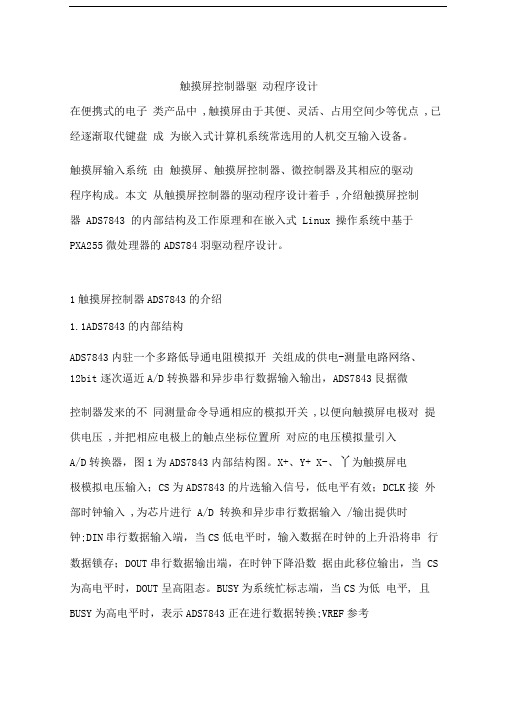
1触摸屏控制器ADS7843的介绍1.1ADS7843的内部结构ADS7843内驻一个多路低导通电阻模拟开关组成的供电-测量电路网络、12bit逐次逼近A/D转换器和异步串行数据输入输出,ADS7843艮据微控制器发来的不同测量命令导通相应的模拟开关 ,以便向触摸屏电极对提供电压 ,并把相应电极上的触点坐标位置所对应的电压模拟量引入A/D转换器,图1为ADS7843内部结构图。
X+、Y+ X-、丫为触摸屏电极模拟电压输入;CS为ADS7843的片选输入信号,低电平有效;DCLK接外部时钟输入 ,为芯片进行 A/D 转换和异步串行数据输入 /输出提供时钟;DIN串行数据输入端,当CS低电平时,输入数据在时钟的上升沿将串行数据锁存;DOUT串行数据输出端,在时钟下降沿数据由此移位输出,当 CS 为高电平时,DOUT呈高阻态。
BUSY为系统忙标志端,当CS为低电平, 且BUSY为高电平时,表示ADS7843正在进行数据转换;VREF参考电压输入端,电压值在+1V到+VCC之间变化;PENIRC为笔触中断,低电平有效;IN3、IN4为辅助ADC转换输入通道;+VCC为电源输入。
图1ADS7843内部结构1.2ADS7843的转换时序ADS7843完成一次数据转换需要与微控制器进行3次通信,第一次微处理器通过异步数据传送向 ADS843 发送控制字 ,其中包括起始位、通道选择、 8/12 位模式、差分 /单端选择和掉电模式选择 ,其后的两次数据传送则是微控制器从 ADS7843 取出 16bitA/D 转换结果数据(最后四位自动补零),每次通信需要 8 个时钟周期 ,完成一次数据转换共需 24 个时钟周期周2为ADS7843转换时序。
ADS7844N数模转换器
©1998 Burr-Brown Corporation PDS-1463D Printed in U.S.A. July, 1999®2ADS7844SPECIFICATION: +5VAt T A = –40°C to +85°C, +V CC = +5V, V REF = +5V, f SAMPLE = 200kHz, and f CLK = 16 • f SAMPLE = 3.2MHz, unless otherwise noted.The information provided herein is believed to be reliable; however, BURR-BROWN assumes no responsibility for inaccuracies or omissions. BURR-BROWN assumes no responsibility for the use of this information, and all use of such information shall be entirely at the user’s own risk. Prices and specifications are subject to change without notice. No patent rights or licenses to any of the circuits described herein are implied or granted to any third party. BURR-BROWN does not authorize or warrant any BURR-BROWN product for use in life support devices and/or systems.SPECIFICATION: +2.7VAt T A = –40°C to +85°C, +V CC = +2.7V, V REF = +2.5V, f SAMPLE = 125kHz, and f CLK = 16 • f SAMPLE = 2MHz, unless otherwise noted.®3ADS7844®4ADS7844PIN CONFIGURATIONTop ViewPIN DESCRIPTIONSPIN NAME DESCRIPTION1CH0Analog Input Channel 0.2CH1Analog Input Channel 1.3CH2Analog Input Channel 2.4CH3Analog Input Channel 3.5CH4Analog Input Channel 4.6CH5Analog Input Channel 5.7CH6Analog Input Channel 6.8CH7Analog Input Channel 7.9COMGround reference for analog inputs. Sets zero code voltage in single ended mode. Connect this pin to ground or ground reference point.10SHDN Shutdown. When LOW, the device enters a very low power shutdown mode.11V REF Voltage Reference Input. See Specification Table for ranges.12+V CC Power Supply, 2.7V to 5V.13GND Ground 14GND Ground15D OUTSerial Data Output. Data is shifted on the falling edge of D CLK . This output is high impedance when CS is high.16BUSYBusy Output. Busy goes low when the DIN control bits are being read and also when the device is converting.The Output is high impedance when CS is High.17D IN Serial Data Input. If CS is LOW, data is latched on rising edge of D CLK .18CSChip Select Input. Active LOW. Data will not be clocked into D IN unless CS is low. When CS is high D OUT is high impedance.19CLK External Clock Input. The clock speed determines the conversion rate by the equation f CLK = 16 • f SAMPLE .20+V CCPower Supply12345678910CH0CH1CH2CH3CH4CH5CH6CH7COMSHDN +V CC D CLK CS D IN BUSY D OUT GND GND +V CC V REF20191817161514131211ADS7844MINIMUM RELATIVE MAXIMUM SPECIFICATION PACKAGE ACCURACYGAIN ERRORTEMPERATUREDRAWING ORDERING TRANSPORTPRODUCT (LSB)(LSB)RANGE PACKAGE NUMBER (1)NUMBER (2)MEDIA ADS7844E±2±4–40°C to +85°C20-Lead QSOP349ADS7844E Rails""""""ADS7844E/2K5Tape and ReelADS7844N"""20-Lead SSOP334ADS7844N Rails""""""ADS7844N/1K Tape and ReelADS7844EB±1±3–40°C to +85°C20-Lead QSOP349ADS7844EB Rails""""""ADS7844EB/2K5Tape and ReelADS7844NB"""20-Lead SSOP334ADS7844NB Rails""""""ADS7844NB/1KTape and ReelNOTES: (1) For detailed drawing and dimension table, please see end of data sheet, or Appendix C of Burr-Brown IC Data Book. (2) Models with a slash (/) are available only in Tape and Reel in the quantities indicated (e.g., /2K5 indicates 2500 devices per reel). Ordering 2500 pieces of “ADS7844/2K5” will get a single 2500-piece Tape and Reel. For detailed Tape and Reel mechanical information, refer to Appendix B of Burr-Brown IC Data Book.PACKAGE/ORDERING INFORMATIONABSOLUTE MAXIMUM RATINGS (1)+V CC to GND ........................................................................–0.3V to +6V Analog Inputs to GND ............................................–0.3V to +V CC + 0.3V Digital Inputs to GND ...........................................................–0.3V to +6V Power Dissipation..........................................................................250mW Maximum Junction Temperature...................................................+150°C Operating Temperature Range ........................................–40°C to +85°C Storage Temperature Range .........................................–65°C to +150°C Lead Temperature (soldering, 10s)...............................................+300°C NOTE: (1) Stresses above those listed under “Absolute Maximum Ratings”may cause permanent damage to the device. Exposure to absolute maximum conditions for extended periods may affect device reliability.This integrated circuit can be damaged by ESD. Burr-Brown recommends that all integrated circuits be handled with appropriate precautions. Failure to observe proper handling and installation procedures can cause damage.ESD damage can range from subtle performance degradation to complete device failure. Precision integrated circuits may be more susceptible to damage because very small parametric changes could cause the device not to meet its published specifi-cations.®5ADS7844TYPICAL PERFORMANCE CURVES:+5VAt T A = +25°C, +V CC = +5V, V REF = +5V, f SAMPLE = 200kHz, and f CLK = 16 • f SAMPLE= 3.2MHz, unless otherwise noted.0–20–40–60–80–100–120FREQUENCY SPECTRUM(4096 Point FFT; f IN = 1,123Hz, –0.2dB)100257550Frequency (kHz)A m p l i t u d e (d B)0–20–40–60–80–100–120FREQUENCY SPECTRUM(4096 Point FFT; f IN = 10.3kHz, –0.2dB)0100257550Frequency (kHz)A m p l i t u d e (dB )SIGNAL-TO-NOISE RATIO AND SIGNAL-TO-(NOISE+DISTORTION) vs INPUT FREQUENCY101100Input Frequency (kHz)S N R a n d S I N A D (d B )74737271706968SPURIOUS FREE DYNAMIC RANGE AND TOTAL HARMONIC DISTORTION vs INPUT FREQUENCY101100Input Frequency (kHz)S F D R (d B )T H D (d B )8580757065–85–80–75–70–6512.011.811.611.411.211.0EFFECTIVE NUMBER OF BITSvs INPUT FREQUENCY101100Input Frequency (kHz)E f f e c t i v e N u m b e r o f B i t sCHANGE IN SIGNAL-TO-(NOISE+DISTORTION)vs TEMPERATURE–20–40100Temperature (°C)D e l t a f r o m +25°C (d B )0.40.20.0–0.2–0.4–0.60.6020406080®6ADS78440–20–40–60–80–100–120FREQUENCY SPECTRUM(4096 Point FFT; f IN = 1,129Hz, –0.2dB)62.515.646.931.3Frequency (kHz)A m p l i t u d e (dB )0–20–40–60–80–100–120FREQUENCY SPECTRUM(4096 Point FFT; f IN = 10.6kHz, –0.2dB)062.515.646.931.3Frequency (kHz)A m p l i t u d e (d B)SIGNAL-TO-NOISE RATIO AND SIGNAL-TO-(NOISE+DISTORTION) vs INPUT FREQUENCY101100Input Frequency (kHz)S N R a n d S I N A D (d B )78747066625854SPURIOUS FREE DYNAMIC RANGE AND TOTAL HARMONIC DISTORTION vs INPUT FREQUENCY101100Input Frequency (kHz)S F D R (d B )T H D (d B )908580757065605550–90–85–80–75–70–65–60–55–50EFFECTIVE NUMBER OF BITSvs INPUT FREQUENCY101100Input Frequency (kHz)E f f e c t i v e N u m b e r o f B i t s12.011.511.010.510.09.59.0TYPICAL PERFORMANCE CURVES:+2.7VAt T A = +25°C, +V CC = +2.7V, V REF = +2.5V, f SAMPLE = 125kHz, and f CLK = 16 • f SAMPLE = 2MHz, unless otherwise noted.CHANGE IN SIGNAL-TO-(NOISE+DISTORTION)vs TEMPERATURE–20–40100Temperature (˚C)D e l t a f r o m +25°C (d B )0.20.0–0.2–0.4–0.6–0.80.4020406080®7ADS7844SUPPLY CURRENT vs TEMPERATURE20–40100–2040Temperature (˚C)S u p p l y C u r r e n t (µA )4003503002502001501006080POWER DOWN SUPPLY CURRENTvs TEMPERATURE20–40100–2040Temperature (˚C)S u p p l y C u r r e n t (n A )140120100806040206080Output Code1.000.750.500.250.00–0.25–0.50–0.75–1.00INTEGRAL LINEARITY ERROR vs CODE800H FFF H000HI L E (L S B)Output Code1.000.750.500.250.00–0.25–0.50–0.75–1.00DIFFERENTIAL LINEARITY ERROR vs CODE800H FFF H000HD LE (L S B )CHANGE IN GAIN vs TEMPERATURE20–40100–2040Temperature (˚C)D e l t a f r o m +25˚C (L S B )0.150.100.050.00–0.05–0.10–0.156080CHANGE IN OFFSET vs TEMPERATURE20–40100–2040Temperature (˚C)D e l t a f r o m +25˚C (L S B )0.60.40.20.0–0.2–0.4–0.66080TYPICAL PERFORMANCE CURVES:+2.7V (CONT)At T A = +25°C, +V CC = +2.7V, V REF = +2.5V, f SAMPLE = 125kHz, and f CLK = 16 • f SAMPLE = 2MHz, unless otherwise noted.®8ADS7844REFERENCE CURRENT vs SAMPLE RATE751252550100Sample Rate (kHz)R e f e r e n c e C u r r e n t (µA )14121086420REFERENCE CURRENT vs TEMPERATURE20–40100–2040Temperature (˚C)R e f e r e n c e C u r r e n t (µA )1816141210866080SUPPLY CURRENT vs +V CC3.5252.54+V CC (V)S u p p l y C u r r e n t (µA )3203002802602402202001804.53MAXIMUM SAMPLE RATE vs +V CC3.5252.54+V CC (V)S a m p l e R a t e (H z )1M100k10k1k4.53TYPICAL PERFORMANCE CURVES (CONT)At T A = +25°C, +V CC = +2.7V, V REF = +2.5V, f SAMPLE = 125kHz, and f CLK = 16 • f SAMPLE = 2MHz, unless otherwise noted.®9ADS7844THEORY OF OPERATIONThe ADS7844 is a classic successive approximation register (SAR) analog-to-digital (A/D) converter. The architecture is based on capacitive redistribution which inherently includes a sample/hold function. The converter is fabricated on a 0.6µs CMOS process.The basic operation of the ADS7844 is shown in Figure 1.The device requires an external reference and an external clock. It operates from a single supply of 2.7V to 5.25V. The external reference can be any voltage between 100mV and +V CC . The value of the reference voltage directly sets the input range of the converter. The average reference input current depends on the conversion rate of the ADS7844.The analog input to the converter is differential and is provided via an eight-channel multiplexer. The input can be provided in reference to a voltage on the COM pin (which is generally ground) or differentially by using four of the eight input channels (CH0 - CH7). The particular configura-tion is selectable via the digital interface.FIGURE 1. Basic Operation of the ADS7844.ANALOG INPUTFigure 2 shows a block diagram of the input multiplexer on the ADS7844. The differential input of the converter is derived from one of the eight inputs in reference to the COM pin or four of the eight inputs. Table I and Table II show the relationship between the A2, A1, A0, and SGL/DIF control bits and the configuration of the analog multiplexer. The control bits are provided serially via the DIN pin, see the Digital Interface section of this data sheet for more details.When the converter enters the hold mode, the voltage difference between the +IN and –IN inputs (see Figure 2) is captured on the internal capacitor array. The voltage on the –IN input is limited between –0.2V and 1.25V, allowing the input to reject small signals which are common to both the +IN and –IN input. The +IN input has a range of –0.2V to +V CC + 0.2V.The input current on the analog inputs depends on the conversion rate of the device. During the sample period, the source must charge the internal sampling capacitor (typi-®10ADS7844cally 25pF). After the capacitor has been fully charged, there is no further input current. The rate of charge transfer from the analog source to the converter is a function of conversion rate.REFERENCE INPUTThe external reference sets the analog input range. The ADS7844 will operate with a reference in the range of 100mV to +V CC . Keep in mind that the analog input is the difference between the +IN input and the –IN input as shown in Figure 2. For example, in the single-ended mode, a 1.25V reference, and with the COM pin grounded, the selected input channel (CH0 - CH7) will properly digitize a signal in the range of 0V to 1.25V. If the COM pin is connected to 0.5V,the input range on the selected channel is 0.5V to 1.75V.There are several critical items concerning the reference input and its wide voltage range. As the reference voltage is re-duced, the analog voltage weight of each digital output code is also reduced. This is often referred to as the LSB (least significant bit) size and is equal to the reference voltage divided by 4096. Any offset or gain error inherent in the A/D converter will appear to increase, in terms of LSB size, as the reference voltage is reduced. For example, if the offset of a given converter is 2 LSBs with a 2.5V reference, then it will typically be 10 LSBs with a 0.5V reference. In each case, the actual offset of the device is the same, 1.22mV.Likewise, the noise or uncertainty of the digitized output will increase with lower LSB size. With a reference voltage of 100mV, the LSB size is 24µV. This level is below the internal noise of the device. As a result, the digital output code will not be stable and vary around a mean value by a number of LSBs. The distribution of output codes will be gaussian and the noise can be reduced by simply averaging consecutive conversion results or applying a digital filter.With a lower reference voltage, care should be taken to provide a clean layout including adequate bypassing, a clean (low noise, low ripple) power supply, a low-noise reference,and a low-noise input signal. Because the LSB size is lower,the converter will also be more sensitive to nearby digital signals and electromagnetic interference.The voltage into the V REF input is not buffered and directly drives the capacitor digital-to-analog converter (CDAC)portion of the ADS7844. Typically, the input current is 13µA with a 2.5V reference. This value will vary by microamps depending on the result of the conversion. The reference current diminishes directly with both conversion rate and reference voltage. As the current from the reference is drawn on each bit decision, clocking the converter more quickly during a given conversion period will not reduce overall current drain from the reference.DIGITAL INTERFACEFigure 3 shows the typical operation of the ADS7844’s digital interface. This diagram assumes that the source of the digital signals is a microcontroller or digital signal processor with a basic serial interface (note that the digital inputs are over-voltage tolerant up to 5.5V, regardless of +V CC ). Each communication between the processor and the converter consists of eight clock cycles. One complete conversion can be accomplished with three serial communications, for a total of 24 clock cycles on the DCLK input.The first eight clock cycles are used to provide the control byte via the DIN pin. When the converter has enough information about the following conversion to set the input multiplexer appropriately, it enters the acquisition (sample)mode. After three more clock cycles, the control byte is complete and the converter enters the conversion mode. At this point, the input sample/hold goes into the hold mode.The next twelve clock cycles accomplish the actual analog-to-digital conversion. A thirteenth clock cycle is needed for the last bit of the conversion result. Three more clock cycles are needed to complete the last byte (DOUT will be LOW).These will be ignored by the converter.Control ByteAlso shown in Figure 3 is the placement and order of the control bits within the control byte. Tables III and IV give detailed information about these bits. The first bit, the ‘S’ bit,must always be HIGH and indicates the start of the control byte. The ADS7844 will ignore inputs on the DIN pin until the start bit is detected. The next three bits (A2 - A0) select the active input channel or channels of the input multiplexer (see Tables I and II and Figure 2).FIGURE 2. Simplified Diagram of the Analog Input.®11ADS7844FIGURE 3. Conversion Timing, 24-Clocks per Conversion, 8-Bit Bus Interface. No DCLK delay required with dedicatedserial port.1DCLKCS8111DOUT BUSYSDIN CONTROL BITSSCONTROL BITS109876543210111098118FIGURE 4. Conversion Timing, 16-Clocks per Conversion, 8-bit Bus Interface. No DCLK delay required with dedicatedserial port.Bit 7Bit 0(MSB)Bit 6Bit 5Bit 4Bit 3Bit 2Bit 1(LSB)SA2A1A0—SGL/DIFPD1PD0TABLE III.Order of the Control Bits in the Control Byte.TABLE IV.Descriptions of the Control Bits within theControl Byte.BIT NAME DESCRIPTION7SStart Bit. Control byte starts with first HIGH bit on DIN. A new control byte starts with every 15th clock cycle.6 - 4A2 - A0Channel Select Bits. Along with the SGL/DIF bit,these bits control the setting of the multiplexer input as detailed in Tables I and II.3—Not Used.2SGL/DIFSingle-Ended/Differential Select Bit. Along with bits A2 - A0, this bit controls the setting of the multiplexer input as detailed in Tables I and II.1 - 0PD1 - PD0Power-Down Mode Select Bits. See Table V for details.The SGL/DIF bit controls the multiplexer input mode: either single-ended (HIGH) or differential (LOW). In single-ended mode, the selected input channel is referenced to the COM pin. In differential mode, the two selected inputs provide a differential input. See Tables I and II and Figure 2 for more information. The last two bits (PD1 - PD0) select the power-down mode as shown in Table V. If both inputs are HIGH,the device is always powered up. If both inputs are LOW, the device enters a power-down mode between conversions.When a new conversion is initiated, the device will resume normal operation instantly—no delay is needed to allow the device to power up and the very first conversion will be valid.16-Clocks per ConversionThe control bits for conversion n+1 can be overlapped with conversion ‘n’ to allow for a conversion every 16 clock cycles, as shown in Figure 4. This figure also shows possible serial communication occurring with other serial peripherals between each byte transfer between the processor and the converter. This is possible provided that each conversion completes within 1.6ms of starting. Otherwise, the signal that has been captured on the input sample/hold may droop enough to affect the conversion result. In addition, the ADS7844 is fully powered while other serial communica-tions are taking place.®12ADS7844Digital TimingFigure 5 and Tables VI and VII provide detailed timing for the digital interface of the ADS7844.15-Clocks per ConversionFigure 6 provides the fastest way to clock the ADS7844.This method will not work with the serial interface of most microcontrollers and digital signal processors as they are generally not capable of providing 15 clock cycles per serial transfer. However, this method could be used with field programmable gate arrays (FPGAs) or application specific integrated circuits (ASICs). Note that this effectively in-creases the maximum conversion rate of the converter be-yond the values given in the specification tables, which assume 16 clock cycles per conversion.PD1PD0DescriptionPower-down between conversions. When each conversion is finished, the converter enters a low power mode. At the start of the next conversion,the device instantly powers up to full power. There is no need for additional delays to assure full operation and the very first conversion is valid.01Reserved for future use.10Reserved for future use.11No power-down between conversions, device al-ways powered.TABLE V. Power-Down Selection.SYMBOL DESCRIPTION MIN TYP MAX UNITS t ACQ Acquisition Time1.5µs t DS DIN Valid Prior to DCLK Rising 100ns t DH DIN Hold After DCLK HIGH 10nst DO DCLK Falling to DOUT Valid 200ns t DV CS Falling to DOUT Enabled 200ns t TR CS Rising to DOUT Disabled 200ns t CSS CS Falling to First DCLK Rising 100ns t CSH CS Rising to DCLK Ignored0ns t CH DCLK HIGH 200ns t CL DCLK LOW200ns t BD DCLK Falling to BUSY Rising 200ns t BDV CS Falling to BUSY Enabled 200ns t BTRCS Rising to BUSY Disabled200nsTABLE VI. Timing Specifications (+V CC = +2.7V to 3.6V,T A = –40°C to +85°C, C LOAD = 50pF).SYMBOL DESCRIPTION MIN TYPMAXUNITS t ACQ Acquisition Time900ns t DS DIN Valid Prior to DCLK Rising 50ns t DH DIN Hold After DCLK HIGH 10ns t DO DCLK Falling to DOUT Valid 100ns t DV CS Falling to DOUT Enabled 70ns t TR CS Rising to DOUT Disabled 70ns t CSS CS Falling to First DCLK Rising 50ns t CSH CS Rising to DCLK Ignored0ns t CH DCLK HIGH 150ns t CL DCLK LOW150ns t BD DCLK Falling to BUSY Rising 100ns t BDV CS Falling to BUSY Enabled 70ns t BTRCS Rising to BUSY Disabled70nsTABLE VII. Timing Specifications (+V CC = +4.75V to+5.25V, T A = –40°C to +85°C, C LOAD = 50pF).FIGURE 6. Maximum Conversion Rate, 15-Clocks per Conversion.FIGURE 5. Detailed Timing Diagram.1DCLKCS 11DOUTBUSY A2SDIN A1A0SGL/DIFPD1PD0109876543210111098765432A1A0151151A2SA1A0SGL/DIFPD1PD0A2Ssupply current for these two cases are shown in Figure 9.from switching power supplies, nearby digital logic, and®13ADS7844®14ADS7844high power devices. The degree of error in the digital output depends on the reference voltage, layout, and the exact timing of the external event. The error can change if the external event changes in time with respect to the DCLK input.With this in mind, power to the ADS7844 should be clean and well bypassed. A 0.1µF ceramic bypass capacitor should be placed as close to the device as possible. In addition, a 1µF to 10µF capacitor and a 5Ω or 10Ω series resistor may be used to lowpass filter a noisy supply.The reference should be similarly bypassed with a 0.1µF capacitor. Again, a series resistor and large capacitor can be used to lowpass filter the reference voltage. If the reference voltage originates from an op amp, make sure that it can drive the bypass capacitor without oscillation (the series resistor can help in this case). The ADS7844 draws very little current from the reference on average, but it does place larger demands on the reference circuitry over short periods of time (on each rising edge of DCLK during a conversion).The ADS7844 architecture offers no inherent rejection of noise or voltage variation in regards to the reference input.This is of particular concern when the reference input is tied to the power supply. Any noise and ripple from the supply will appear directly in the digital results. While high fre-quency noise can be filtered out as discussed in the previous paragraph, voltage variation due to line frequency (50Hz or 60Hz) can be difficult to remove.The GND pin should be connected to a clean ground point.In many cases, this will be the “analog” ground. Avoid connections which are too near the grounding point of a microcontroller or digital signal processor. If needed, run a ground trace directly from the converter to the power supply entry point. The ideal layout will include an analog ground plane dedicated to the converter and associated analog circuitry.。
基于ADS7843的触摸屏控制系统设计

Science &Technology Vision科技视界0引言在电子产品及工业产品的设计中,触摸屏由于其轻便、占用空间少、方便灵活等优点越来越受到设计师及用户的青睐。
触摸屏可作为模拟键盘,使用起来比普通键盘灵活,因为键的位置可根据需要进行改变,并且省去了按键所占用的空间。
触摸屏分为电阻、电容、表面声波、红外线扫描和矢量压力传感等,其中四线电阻触摸屏应用广泛。
1ADS7843简介ADS7843是一款专为四线电阻触摸屏设计的带SPI 接口的12位AD 转换器,内部含模拟电子开关和逐次比较型AD 转换器。
当要采样Y 方向的AD 值时,通过将Y+、Y 一端施加电压,将X+送入AD 转换器得到Y 方向的AD 值;同理可得X 方向的AD 值。
而这些转换均由MCU 通过SPI 方式向ADS7843发送命令来完成。
ADS7843的引脚功能如表1所示。
表1ADS7843的引脚功能ADS7843之所以能实现对触摸屏的控制,是因为其内部结构很容易实现电极电压的切换,并能进行快速A/D 转换。
内部结构如图1所示,A2~A0和SER 为控制寄存器中的控制位,用来进行开关切换和参考电压的选择。
图1ADS7843内部结构2触摸屏控制系统设计以应用广泛的STC89C52作为主控制器,进行触摸控制系统设计。
2.1硬件接口电路设计ADS7843串行接口的一次完整操作需要3×8=24个DCLK 时钟周期,前8个脉冲接收8位的命令,并在第6个脉冲的上升沿开始A/D 转换器进入采样阶段,从第9个脉冲开始进入转换阶段,输出,输出12位采样值,转换结束进入空闲阶段。
直到24个DCLK 结束,CS 置高电平,一次测量结束。
ADS7843采用、转换时序如图2所示。
图2ADS7843采用、转换时序ADS7843与STC89C52的连接图如图3所示。
图3ADS7843与STC89C52的连接图2.2软件设计当用户在触摸屏上的有效区域内点击时,触摸屏的X 方向、Y 方向输出电阻分别随X 和Y 呈线性变化,ADS7843控制器将其分别转换为12位数据,通过中断告知STC89C52需要接收数据,STC89C52接收到数据后进行处理;首先进行触点数据是否有效判断,包括两方面:一是判断是否误操作,即是否是由于人的抖动产生的错误数据;二是ADS7843传过来得数据是否有效,由于刚开始的传过来的第一个基于ADS7843的触摸屏控制系统设计薛大为杨春兰(蚌埠学院机械与电子工程系,安徽蚌埠233030)【摘要】触摸屏在现代电子设备中广泛使用。
ads7843中文资料
•’—•p 应用与设计¡¤³—˜”“触摸屏接口解放军信息工程大学胡冰吴升艳岳春生Touch Scre e n Inte r f a ce Ch i p ADS7843¨Õ¢ÉÎÇ·Õ³ÈÅÎÇÙÁιÕÅ£ÈÕÎÓÈÅÎÇ摘要š简单介绍了¡¤³—˜”“的功能特点和工作原理Œ探讨了¡¤³—˜”“触摸屏接口芯片的模式选择和应用技巧Œ最后给出了基于该系统的一个实际使用方案"关键词š触摸屏控制器›嵌入式系统›¡¤³—˜”“分类号š´°’—“文献标识码š¢文章编号š‘••–•–™——ˆ’••’‰•—•••’—••“图‘¡¤³—˜”“的连接关系¡¤³—˜”“触摸屏接口‘前言随着生活中类似于°¤¡的手持设备的越来越多Œ彩色¬£¤触摸屏也变得越来越普及Œ并逐渐成为当今的主流配置"触摸屏分为电阻!电容!表面声波!红外线扫描和矢量压力传感等Œ其中使用最多的是四线或五线电阻触摸屏"四线电阻触摸屏是由两个透明电阻膜构成的Œ在它的水平和垂直电阻网上施加电压Œ就可通过¡•¤转换面板在触摸点测量出电压Œ从而对应出坐标值"本文除了简单介绍¡¤³—˜”“的特点和原理之外Œ主要讨论触摸屏控制器的使用技巧Œ同时给出了具体的应用连接图"’¡¤³—˜”“的功能特性¡¤³—˜”“是´©公司生产的”线电阻触摸屏转换接口芯片"它是一款具有同步串行接口的‘’位取样模数转换器"在‘’•Ë¨Ú吞吐速率和’Ž—¶电压下的功耗为—••L ·Œ而在关闭模式下的功耗仅为•Ž•L ·"因此Œ¡¤³—˜”“以其低功耗和高速率等特性Œ被广泛应用在采用电池供电的小型手持设备上"¡¤³—˜”“采用³³¯°•‘–引脚封装形式Œ温度范围是•”•*‹˜•e "¡¤³—˜”“具有两个辅助输入ˆ©®“!©®”‰Œ可设置为˜位或‘’位模式"其外部连接电路如图‘所示Œ该电路的工作电压¶ÃÃ在’Ž—*•Ž’•¶之间Œ基准电压¶ÒÅÆ介于‘¶*‹¶ÃÃ"该电路的基准电压确定了转换器的输入范围Œ输出数据中每个数字位代表的模拟电压等于基准电压除以”•™–"平均基准输入电流由¡¤³—˜”“的转换率来确定"以下是¡¤³—˜”“的主要引脚功能š¸‹!¹‹!¸•!¹•š转换器模拟输入端Œ实际上是一个”通道多路器›¤£¬«š外部时钟输入引脚›£³š片选端›参考文献‘Ž张芳兰Ž´-³“’•£’ØØ用户指南Ž电子工业出版社Œ‘™™™Ž–’Ž赵保经Ž¡•¤和¤•¡转换器应用手册Ž上海科学普及出版社Œ‘™™•“Ž-ÁØÉÍŽ‹•¶³ÉÎÇÌÅ•³ÕÐÐÌÙŒ‘-ÓÐÓŒ‘–•¢ÉÔ³ÅÌÆ•£ÁÌÉÂÒÁÔÉÎÇ¡¤£Œ’•••”Ž闻亭公司Ž´-³“’•£’¸¸高速数字信号处理器原理与应用Ž‘™™˜Œ”•Ž´ÅØÁÓ©ÎÓÔÒÕÍÅÎÔÓ©ÎÃŽ´-³“’•£’•ØµÓÅÒ‡Ó§ÕÉÄÅŒ‘™™™收稿日期š’••‘•‘’•’‘咨询编号š•’•—‘•海纳电子资讯网:www.fpga-arm.com 为您提供各种IC中文资料•’˜•5国外电子元器件6’••’年第—期’••’年—月¤©®š串行输入Œ其控制数据通过该引脚输入›¤¯µ´š串行数据输出Œ用于输出转换后的触摸位置数据Œ最大数为二进制的”•™•›©®“!©®”š辅助输入引脚›°¥®©²±š°¥®中断引脚Œ可用于在触摸显示屏后引发一个中断"“工作原理¡¤³—˜”“是一款连续近似记录ˆ³¡²‰的¡•¤转换器"可通过连结触摸屏¸‹将触摸信号输入到¡•¤转换器Œ同时打开¹‹和¹•驱动Œ然后数字化¸‹的电压Œ从而得到当前¹位置的测量结果"同理也可得到¸方向的坐标"具体设置和使用方法可查阅´©公司的¡¤³—˜”“数据手册Œ下面主要介绍¡¤³—˜”“的模式设置!°¥®中断引脚的使用和软件编程方法"“Ž‘模式设置¡¤³—˜”“有差分ˆ¤©¦¦¥²¥®´©¡¬‰和单端ˆ³©®2§¬¥•¥®¤¥¤-¯¤¥‰两种工作模式"这两种模式对转换后的精度和可靠性有一些影响"如果将¡•¤转换器配置为读绝对电压ˆ单端模式‰方式Œ那么驱动ˆ¤²©¶¥²‰电压的下降将导致转换输入数据的错误"而如果配置为差分模式Œ则可以避免上述错误"当触摸屏被按下时Œ有两种情况可影响接触点的电压š一种是当触摸到显示屏时Œ会导致触摸屏外层振动›另一种是触摸屏顶层和低层之间的寄生电容引起的电流振荡以及在¡¤³—˜”“输入引脚上引起的电压振荡"这两种情况都可导致触摸屏上的电压发生振荡以及增加¤£值稳定的时间"在单端模式中Œ一旦在触摸屏上检测到一次触摸事件Œ电路系统将发送一串控制字节给¡¤³—˜”“Œ并要求它进行一次转换"然后¡¤³—˜”“将在获取周期的起始点通过内部¦¥´开关给面板提供电压Œ而这将导致触摸点电压的升高"正如上面所介绍的Œ上升的电压在最终稳定之前会振荡一段时间"当获取周期结束后Œ所有的¦¥´开关关闭Œ¡•¤转换器进入转换周期"如果在转换周期期间Œ没有发出下一个控制字节Œ¡¤³—˜”“将进入低功耗模式并等待下一条指令"由于面板上分布有大量电容Œ特别是滤波噪音Œ因此Œ应该注意设置好对应于¸坐标或¹坐标上的电压"在单端模式中Œ输入电压必须在¤ÁÔÁ©Î×ÏÒÄ的最后三个时钟周期期间设置Œ否则将产生错误"除了内部¦¥´开关从获取周期开始到转换周期结束期间一直保持打开状态以外Œ差分模式的操作类似于单端模式"加在面板上的电压将成为¡•¤转换器的基准电压Œ提供一个度量比操作"这意味着如果加在面板上的电压发生变化ˆ由于电源!驱动电阻!温度或触摸屏电阻等原因‰Œ¡•¤转换器的度量比操作将对这种变化进行补偿"如果在当前转换周期发向¡¤³—˜”“的下一个控制字节所选择的通道与前一个控制字节相同Œ那么在当前转换完成后开关仍然不会关闭"在这两种模式中Œ¡¤³—˜”“只有“个时钟周期可以从触摸屏上获取ˆ取样‰输入模拟电压Œ因此Œ为了¡¤³—˜”“可以获取正确的电压Œ输入电压必须在“个时钟周期的时间范围内设置好"打开驱动将引起触摸屏的电压快速升高到最终值"为了得到正确的转换数据Œ获取必须在触摸屏完全设置好时完成"获取的方式有两种š一种是采用单端模式Œ即采用相对较慢的时钟扩展获取时间ˆ三个时钟周期‰›二是采用差分模式Œ即用相对较快的时钟在第一个转换周期内设置电压Œ在第二个转换周期获取准确电压"该方式的两个控制字节相同Œ且内部¸•¹开关在首次转换后不会关闭"由于首次转换期间电压还不稳定Œ因此应当丢弃首次转换的结果"使用第二种方式的另一个优点是功耗低"因为在全部转换后Œ¡¤³—˜”“会进入低功耗模式来等待下一次取样周期›对于慢时钟Œ下一次取样可能在当前转换结束后立即进入取样周期Œ而没有时间进入低功耗模式"实际在单端模式下不能使用快速时钟"差分模式还具有以下两个优点š第一个优点是能够在不扩展转换器获取时间的条件下用很长的设置时间处理触摸屏Œ即触摸屏电压可以有足够的时间稳定下来"第二个优点是¡¤³—˜”“通过快速时钟可以进入低功耗模式Œ从而可以节约电池能量"因此Œ通常建议使用差分模式"“Ž’°¥®中断引脚的使用°¥®中断引脚的主要作用是让设计者可以完全控制¡¤³—˜”“的低功耗操作模式"图’所示是其模式操作连接示意图"图中Œ©•¯‘和©•¯’是引自¥°—’‘’的通用目的输入•输出口"当电源加入系统且转换器被设置ˆ°¤‘Œ°¤••••‰之后Œ器件进入低功耗模式"而当未触摸面板时Œ¡¤³—˜”“内部的二极海纳电子资讯网:www.fpga-arm.com 为您提供各种IC中文资料•’™•¡¤³—˜”“触摸屏接口图“采用判断两次的方法来克服触摸屏信号的抖动图”采用最后的结果来克服触摸屏信号的抖动图’¡¤³—˜”“ˆ°¤•Œ°¤‘•••‰下的示意图管没有偏压Œ因此没有电流流过ˆ忽略漏流‰›当触摸面板时Œ¹•将提供一条电流ˆ©‰通路Œ这时¸‹!¸•和¹‹处于高阻状态Œ电流经过‘••Ë8电阻和中断二极管Œ°¥®©²±被拉低Œ从而通过©•¯’上一个不超过•Ž–•¶的电压唤醒£°µŒ然后¥°—’‘’再拉低©•¯‘和©•¯’上的电位Œ同时对¡¤³—˜”“控制寄存器写一个字节以进行转换初始化"为了转换°¥®©²±二极管上的偏置电压Œ¥°—’‘’必须拉低©•¯‘和©•¯’上的电压"否则Œ如果在转换期间二极管上有一个前向偏压Œ那么附加的电流将引起错误的输入数据"“Ž“错误触发由于¸‹输入引脚与°¥®中断输出相连Œ因此在¸‹上的噪声可能引起触摸屏的错误触发"设计时可以在°¥®中断输出引脚上连结一个²£滤波器ˆ可对地连结一个‘8的电阻和一个•Ž•‘L ¦的电容‰Œ以过滤噪声脉冲并避免错误触发"“Ž”差分模式下的软件流程图“和图”所示的两种算法假设¡¤³—˜”“配置成差分模式Œ每次转换为‘–个时钟Œ¸轴坐标的结果在¤¡´¡¸中Œ¹轴的坐标在¤¡´¡¹中"其中图“的例子采用的是判断两次的方法来克服触摸屏信号的抖动"¤¡´¡‘用于存储当前转换的结果Œ¤¡´¡’用于存储上一次转换的结果Œ当两次结果相同时Œ转换数据有效"但是Œ应当注意š当输入电压的振动频率和取样频率相近时Œ可能会漏掉正确结果"图”的例子是将最后的转换结果ˆ第Î次‰作为有效转换"可以看出š该方式更加简单Œ但该方法只对某一类触摸屏有效Œ且/Î0的具体值依赖于¡¤³—˜”“输入电压的设置时间Œ同时Œ在确定/Î0值以前还需要对一些触摸屏进行测试"参考文献‘Ž刘永智Œ杨开愚Ž液晶显示技术Ž电子科技大学出版社’Ž¡¤³—˜”“¤ÁÔÁÓÈÅÅÔ´©Œªµ¬¹Œ’••‘收稿日期š’••‘•‘’•’•咨询编号š•’•—‘‘海纳电子资讯网:www.fpga-arm.com 为您提供各种IC中文资料。
- 1、下载文档前请自行甄别文档内容的完整性,平台不提供额外的编辑、内容补充、找答案等附加服务。
- 2、"仅部分预览"的文档,不可在线预览部分如存在完整性等问题,可反馈申请退款(可完整预览的文档不适用该条件!)。
- 3、如文档侵犯您的权益,请联系客服反馈,我们会尽快为您处理(人工客服工作时间:9:00-18:30)。
LCALL AD_RUN
MOV CHYAdResultH,AD_RESULTH
MOV CHYAdResultL,AD_RESULTL
RET
; A/D转换子程序(AD_RUN)
;输入: AD_CH-模式和通道选择命令字
;输出: AD_RESULTH,L ;12 bit的A/D转换值
2 M68VZ328ADS Application Development System User's Manual. Revision 1.4. 2000
3 Burr-Brown IC Data Book
触摸屏的工作原理及典型应用
摘要简要介绍触摸屏的结构及工作原理,并以Burr-Brown公司的触摸屏控制芯片ADS7843为例,介绍触摸屏应用的典型电路和操作。由于ADS7843内置12位A/D,理论上触摸屏的输入坐标识别精度为有效长宽的1/4096。
关键词触摸屏ITO ADS7843嵌入式系统
1触摸屏的基本原理
RL A
DJNZ R2,AD_LOOP
NOP
NOP
NOP
NOP
ADW0: JNB BUSY,AD_WAIT ;等待转换完成
SJMP ADW1
AD_WAIT:
LCALL WATCHDOG
NOP
SJMP ADW0
CLR DIN
ADW1: MOV R2,#12 ;开始读取12bit结果
SETB DCLK
CLR DCLK
CHYAdResultL EQU 3BH
;采集通道CHX+的程序段(CHXAD)
CHXAD: MOV AD_CH,#CHX
LCALL AD_RUN
MOV CHXAdResultH,AD_RESULTH
MOV CHXAdResultL,AD_RESULTL
RET
;采集通道CHY+的程序段(CHYAD)
图5 ADS7843内部结构
ADS7843支持两种参考电压输入模式:一种是参考电压固定为VREF,另一种采取差动模式,参考电压来自驱动电极。这两种模式分别如图6(a)、(b)所示。采用图6(b)的差动模式可以消除开关导通压降带来的影响。表2和表3为两种参考电压输入模式所对应的内部开关状况。
图6参考电压输Βιβλιοθήκη 模式2.1 ADS7843的基本特性与典型应用
ADS7843是一个内置12位模数转换、低导通电阻模拟开关的串行接口芯片。供电电压2.7~5 V,参考电压VREF为1 V~+VCC,转换电压的输入范围为0~ VREF,最高转换速率为125 kHz。ADS7843的引脚配置如图3所示。表1为引脚功能说明,图4为典型应用。
表4 ADS7843的控制字Y=0X90 X=0XD0
为了完成一次电极电压切换和A/D转换,需要先通过串口往ADS7843发送控制字,转换完成后再通过串口读出电压转换值。标准的一次转换需要24个时钟周期,如图7所示。由于串口支持双向同时进行传送,并且在一次读数与下一次发控制字之间可以重叠,所以转换速率可以提高到每次16个时钟周期,如图8所示。如果条件允许,CPU可以产生15个CLK的话(比如FPGAs和ASICs),转换速率还可以提高到每次15个时钟周期,如图9所示。
; A/D接口控制线
DCLK BIT P1.3
CS BIT P1.4
DIN BIT P1.5
BUSY BIT P1.6
DOUT BIT P1.7
; A/D通道选择命令字和工作寄存器
CHX EQU 094H ;通道X+的选择控制字
CHY EQU 0D4H;通道Y+的选择控制字
CH3 EQU0A4H
CH4 EQU 0E4H
;使用: R2 ;辅助工作寄存器
AD_RUN:
CLR CS ;芯片允许
CLR DCLK
MOV R2,#8 ;先写8 bit命令字
MOV A,AD_CH
AD_LOOP:
MOV C, ACC.7
MOV DIN,C ;时钟上升沿锁存DIN
SETB DCLK ;开始发送命令字
CLR DCLK ;时钟脉冲,一共24个
图7 A/D转换时序(每次转换需24个时钟周期)
图8 A/D转换时序(每次转换需16个时钟周期)
图9 A/D转换时序(每次转换需15个时钟周期)
2.4 A/D转换时序的程序设计
ADS7843的典型应用如图4所示。假设μP接口与51单片机的P1.3~P1.7相连,现以一次转换需24个时钟周期为例,介绍A/D转换时序的程序设计。
图2工作时的导体层
2触摸屏的控制实现
现在很多PDA应用中,将触摸屏作为一个输入设备,对触摸屏的控制也有专门的芯片。很显然,触摸屏的控制芯片要完成两件事情:其一,是完成电极电压的切换;其二,是采集接触点处的电压值(即A/D)。本文以BB(Burr-Brown)公司生产的芯片ADS7843为例,介绍触摸屏控制的实现。
图1触摸屏结构
触摸屏工作时,上下导体层相当于电阻网络,如图2所示。当某一层电极加上电压时,会在该网络上形成电压梯度。如有外力使得上下两层在某一点接触,则在电极未加电压的另一层可以测得接触点处的电压,从而知道接触点处的坐标。比如,在顶层的电极(X+,X-)上加上电压,则在顶层导体层上形成电压梯度,当有外力使得上下两层在某一点接触,在底层就可以测得接触点处的电压,再根据该电压与电极(X+)之间的距离关系,知道该处的X坐标。然后,将电压切换到底层电极(Y+,Y-)上,并在顶层测量接触点处的电压,从而知道Y坐标。
结束语
在许多嵌入式系统中,CPU提供专门的模块来支持液晶显示和触摸屏的输入,使得接口非常简单。比如,MOTOROLA的MC68VZ328(称为Dragon Ball)就提供专门的引脚来支持8位和4位的液晶显示,对触摸屏的支持通过SPI2借助ADS7843也很容易完成。
参考文献
1 MC68VZ328 Integrated Processor User's Manual
表2参考电压非差动输入模式(SER/DFR="1")
表3参考电压差动输入模式(SER/DFR="0")
2.3 ADS7843的控制字及数据传输格式
ADS7843的控制字如表4所列,其中S为数据传输起始标志位,该位必为"1"。A2~A0进行通道选择(见表2和3)。MODE用来选择A/D转换的精度,"1"选择8位,"0"选择12位。SER/选择参考电压的输入模式(见表2和3)。PD1、PD0选择省电模式:"00"省电模式允许,在两次A/D转换之间掉电,且中断允许;"01"同"00",只是不允许中断;"10"保留;"11"禁止省电模式。
图3 ADS7843引脚
表1引脚功能说明
图4 ADS7843的典型应用
2.2 ADS7843的内部结构及参考电压模式选择
ADS7843之所以能实现对触摸屏的控制,是因为其内部结构很容易实现电极电压的切换,并能进行快速A/D转换。图5所示为其内部结构,A2~A0和SER/为控制寄存器中的控制位,用来进行开关切换和参考电压的选择。
IGNORE:
SETB DCLK
CLR DCLK
DJNZ R2,IGNORE
SETB CS ;禁止芯片
ANL AD_RESULTH,#0FH ;屏蔽高4 bit
RET
2.5 A/D转换结果的数据格式
ADS7843转换结果为二进制格式。需要说明的是,在进行公式计算时,参考电压在两种输入模式中是不一样的。而且,如果选取8位的转换精度,1LSB=VREF/256,一次转换完成时间可以提前4个时钟周期,此时串口时钟速率也可以提高一倍。
典型触摸屏的工作部分一般由三部分组成,如图1所示:两层透明的阻性导体层、两层导体之间的隔离层、电极。阻性导体层选用阻性材料,如铟锡氧化物(ITO)涂在衬底上构成,上层衬底用塑料,下层衬底用玻璃。隔离层为粘性绝缘液体材料,如聚脂薄膜。电极选用导电性能极好的材料(如银粉墨)构成,其导电性能大约为ITO的1000倍。
AD_READ:
SETB DCLK
CLR DCLK ;用时钟的下降沿读取
MOV A,AD_RESULTL
MOV C,DOUT
RLC A
MOV AD_RESULTL,A
MOV A,AD_RESULTH
RLC A
MOV AD_RESULTH,A
DJNZ R2,AD_READ
MOV R2,#4 ;最后是没用的4个时钟
AD_CH EQU 35H ;通道选择寄存器
AD_RESULTH EQU 36H ;存放12 bit A/D值
AD_RESULTL EQU 37H
;存放通道CHX+的A/D值
CHXAdResultH EQU 38H
CHXAdResultL EQU 39H
;存放通道CHY+的A/D值
CHYAdResultH EQU 3AH