
数字集成电路复习习题库
数字电路复习题
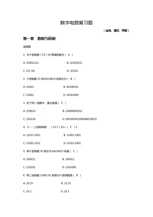
数字电路复习题(选择、填空、判断)第一章数制与码制选择题1.与十进制数(53)10等值的数为(A )A.(100111)2B.(110101)2C.(25 )16D.(33)162.十进制数25用8421BCD码表示为(B )A.10101B.00100101C.11001D.101010003.在下列一组数中,最大数是(C )A.(258)10B.(100000010)2C.(103)16D.(001001011000)8421BCD4.十----二进制转换:(25.7)10=(C )2A.11011.1011B.11001.1001C.11001.1011D.11011.10015.将十进制数35表示为8421BCD码是(C )A.100011B.100011C.110101D.11010006.将二进制数11001.01转换为十进制数是(B )A.20.25B.25.25C.25.2D.25.17.十——二进制转换:(117)10=(A )2A.1110101B.1110110C.1100101D.110101判断题1.数字信号是离散信号,模拟信号是连续信号。
(√)2.格雷码具有任何相邻码只有一位码元不同的特性。
(√)3.8421码又称BCD码,是十进制代码中最常用的一种。
8421码属于恒权码。
(√)4.直接对模拟量进行处理的电子线路称为数字电路。
(X )填空题1.自然界物理量按其变化规律的特点可分为两类,为模拟量和数字量。
2. 数字信号的特点是在时间上和数量上都是离散变化的。
3.(167)10=(10100111)2 =(000101100111)8421BCD。
4.(193)10=(C1 )16 =(000110010011 )8421BCD。
5.二进制数01011001对应的十六进制数(59 )16 ,表示十进制数是89 。
6.BCD余3码100001011001对应的十进制数526 ,表示成BCD8421码是010********* 。
数字集成电路测试题

A 衬底 B 扩散区 C 有源区 D 接触孔和通孔
© Digital Integrated Circuits2nd
提交
Inverter
单选题 1分 最符合阈值电压定义的说法是 。
A 漏端电流为1μA时的栅源电压
B 漏端电流10倍于泄露电流时的栅源电压
衬底载流子浓度和有源区载流子浓度相 C 等时的栅源电压
芯片中的金属线和PCB中的金属线一样, A 可以是多层的。
B
CMOS集成电路是在一块正方形的硅片 上制造的。
光刻机的作用是通过激光在硅片上刻画 C 集成电路版图。
光刻胶的作用是将集成电路所需的不同 D 材料层胶合在一起。
© Digital Integrated Circuits2nd
提交
Inverter
D MOgrated Circuits2nd
提交
Inverter
单选题 1分 电路互连线上的延时td 与长度L的关系是 。
A
td L
B
td L2
C
td L3/2
D
td L3
© Digital Integrated Circuits2nd
数字集成电路 ch1-ch4习题集
Jan M. Rabaey Anantha Chandrakasan Borivoje Nikolic
© Digital Integrated Circuits2nd
Inverter
单选题 1分
在集成电路0.25μm工艺中,晶体管的最小沟 道长度由 决定。
A 光刻精度 B 消费者和代工厂 C 电路工程师 D 电源电压
C 无穷大的“断开”电阻和有限的“导通”电阻。
© Digital Integrated Circuits2nd
数字集成电路习题

带入延迟公式可得,反相器链的延迟
t p N t p 0 (1
N
F
) 5 70 ps (1
5
2000 ) 1960 ps 2ns 1
c. 方法 a 的延迟时间
t p t p 0 (1
j 1
N
C g , j 1
C g , j
) t p 0 (1
解:VGS=VDS=2.5V,管子工作在饱和区。 栅沟电容 CGC=W*L*Cox=0.36um*0.24um*6fF/um2=0.52fF 栅与源漏区的交叠电容 Cov=CGSO=CGDO=W*Co=0.36um*0.31fF/um=0.11fF 栅电容 CG=CGC+2Cov=0.52 fF +2*0.11 fF=0.74fF 栅源电容 CGS=2CGC/3+Cov=2*0.52fF/3+0.11=0.46fF 栅漏电容 CGD=Cov=0.11fF 管子的源区和衬底都接地,所以源衬底扩散结处于零偏状态。有 Cs,bottom=W*LD*Cj0=0.36um*0.625um*2fF/um2=0.45fF Cs,sw=(W+2LD)*Cjsw0=(0.36um+2*0.625um)*0.28um/fF=0.45fF CSB= Cs,bottom + Cs,sw =0.45fF+0.45fF=0.9fF 管子的漏区接 2.5V,衬底接地,所以漏衬底扩散结处于反偏状态。有 CD,bottom=W*LD*Cj0/(1-VD/φ b)mj =0.36um*0.625um*2(fF/um2)/[1-(-2.5V)/0.9V]0.5 =0.23fF CD,sw=(W+2LD)*Cjsw0/(1-VD/φ bsw)mjsw =(0.36um+2*0.625um)*0.28(um/fF)/[1-(-2.5V)/0.9]0.44 =0.25fF CDB= CD,bottom + CD,sw =0.23fF+0.25fF=0.48fF
数字集成电路习题(第三章)

0. Explain qualitatively
4
Chapter 3 Problem Set a. Write down the equations (and only those) which are needed to determine the voltage at node X. Do NOT plug in any values yet. Neglect short channel effects and assume that λp = 0. b. Draw the (approximative) load lines for both MOS transistor and resistor. Mark some of the significant points. c. Determine the required width of the transistor (for L = 0.25µm) such that X equals 1.5 V. d. We have, so far, assumed that M1 is a long-channel device. Redraw the load lines assuming that M1 is velocity-saturated. Will the voltage at X rise or fall?
Table 0.2 Measurements taken from the MOS device, at different terminal voltages.
Measurement number 1 2 3 4 5 6 7 8.
VGS (V) -2.5 1 -0.7 -2.0 -2.5 -2.5 -2.5
R1 = 2kΩ + 2.5 V – ID R2 = 2kΩ
数字集成电路--电路、系统与设计(第二版)课后练习题第六.
数字集成电路--电路、系统与设计(第⼆版)课后练习题第六.Digital Integrated Circuits - 2nd Ed 11 DESIGN PROJECT Design, lay out, and simulate a CMOS four-input XOR gate in the standard 0.25 micron CMOS process. You can choose any logic circuit style, and you are free to choose how many stages of logic to use: you could use one large logic gate or a combination of smaller logic gates. The supply voltage is set at 2.5 V! Your circuit must drive an external 20 fF load in addition to whatever internal parasitics are present in your circuit. The primary design objective is to minimize the propagation delay of the worst-case transition for your circuit. The secondary objective is to minimize the area of the layout. At the very worst, your design must have a propagation delay of no more than 0.5 ns and occupy an area of no more than 500 square microns, but the faster and smaller your circuit, the better. Be aware that, when using dynamic logic, the precharge time should be made part of the delay. The design will be graded on themagnitude of A × tp2, the product of the area of your design and the square of the delay for the worst-case transition.。
数字集成电路--电路、系统与设计(第二版)课后练习题 第六章 CMOS组合逻辑门的设计
Chapter 6 Problem Set
Chapter 6 PROBLEMS
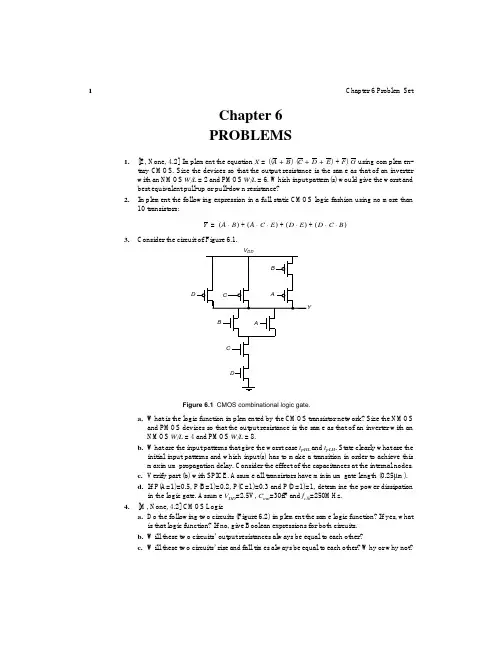
1. [E, None, 4.2] Implement the equation X = ((A + B) (C + D + E) + F) G using complementary CMOS. Size the devices so that the output resistance is the same as that of an inverter with an NMOS W/L = 2 and PMOS W/L = 6. Which input pattern(s) would give the worst and best equivalent pull-up or pull-down resistance? Implement the following expression in a full static CMOS logic fashion using no more than 10 transistors: Y = (A ⋅ B) + (A ⋅ C ⋅ E) + (D ⋅ E) + (D ⋅ C ⋅ B) 3. Consider the circuit of Figure 6.1.
2
VDD E 6 A A 6 B 6 C 6 D 6 E F A B C D 4 4 4 4 E 1 A B C D 4 4 4 4 E 1 6 F 6 B 6 C 6 D
Chapter 6 Problem Set
VDD 6
Circuit A
Circuit B
Figure 6.2 Two static CMOS gates.
【精品】数字集成电路电路、系统与设计第二版课后练习题第六章CMOS组合逻辑门的设计
【精品】数字集成电路--电路、系统与设计(第二版)课后练习题第六章CMOS组合逻辑门的设计第六章 CMOS组合逻辑门的设计1.为什么CMOS电路逻辑门的输入端和输出端都要连接到电源电压?CMOS电路采用了MOSFET(金属氧化物半导体场效应管)作为开关元件,其中N沟道MOSFET(NMOS)和P沟道MOSFET(PMOS)分别用于实现逻辑门的输入和输出。
NMOS和PMOS都需要连接到电源电压,以使其能够正常工作。
输入端连接到电源电压可以确保信号在逻辑门中正常传递,输出端连接到电源电压可以确保输出信号的正确性和稳定性。
2.为什么在CMOS逻辑门中要使用两个互补的MOSFET?CMOS逻辑门中使用两个互补的MOSFET是为了实现高度抗干扰的逻辑功能。
其中,NMOS和PMOS分别用于实现逻辑门的输入和输出。
NMOS和PMOS的工作原理互补,即当NMOS导通时,PMOS截止,当PMOS导通时,NMOS截止。
这样的设计可以在逻辑门的输出上提供高电平和低电平的稳定性,从而提高逻辑门的抗干扰能力。
3.CMOS逻辑门的输入电压范围是多少?CMOS逻辑门的输入电压范围通常是在0V至电源电压之间,即在低电平和高电平之间。
在CMOS逻辑门中,低电平通常定义为输入电压小于0.3Vdd(电源电压的30%),而高电平通常定义为输入电压大于0.7Vdd(电源电压的70%)。
4.如何设计一个基本的CMOS逻辑门?一个基本的CMOS逻辑门可以由一个NMOS和一个PMOS组成。
其中,NMOS的源极连接到地,栅极连接到逻辑门的输入,漏极连接到PMOS的漏极;PMOS的源极连接到电源电压,栅极连接到逻辑门的输入,漏极连接到输出。
这样的设计可以实现逻辑门的基本功能。
5.如何提高CMOS逻辑门的速度?可以采取以下方法来提高CMOS逻辑门的速度:•减小晶体管的尺寸:缩小晶体管的尺寸可以减小晶体管的电容和电阻,从而提高逻辑门的响应速度。
•优化电源电压:增加电源电压可以提高晶体管的驱动能力,从而加快逻辑门的开关速度。
复习题(数电答案)
1.下列四种类型的逻辑门中,可以用( D )实现与、或、非三种基本运算。
A. 与门 B. 或门 C. 非门 D. 与非门 2. 根据反演规则,CD C B A F ++=)(的反函数为(A )。
A. ))((''''''D C C B A F ++= B. ))((''''''D C C B A F ++= C. ))((''''''D C C B A F += D. ))(('''''D C C B A F ++= 3.逻辑函数F=)(B A A ⊕⊕ =( A )。
A. BB. AC. B A ⊕D. B A ⊕4. 最小项ABCD 的逻辑相邻最小项是( A )。
A. ABCDB. ABCDC. ABCDD. ABCD 5. 对CMOS 与非门电路,其多余输入端正确的处理方法是(D )。
A. 通过大电阻接地(>1.5K Ω)B. 悬空C. 通过小电阻接地(<1K Ω)D. 通过电阻接+VCC 6. 下列说法不正确的是( C )。
A .当高电平表示逻辑0、低电平表示逻辑1时称为正逻辑。
B .三态门输出端有可能出现三种状态(高阻态、高电平、低电平)。
C .OC 门输出端直接连接可以实现正逻辑的线与运算。
D .集电极开路的门称为OC 门。
7.已知74LS138译码器的输入三个使能端(E 1=1, E 2A = E 2B =0)时,地址码A 2A 1A 0=011,则输出 Y 7 ~Y 0是( C ) 。
A. 11111101B. 10111111C. 11110111D. 111111118. 若用JK 触发器来实现特性方程为1+n QQ AB Q +=A ,则JK 端的方程为( A )。
A.J=AB ,K=AB.J=AB ,K=AC. J =A ,K =ABD.J=B A ,K=AB 9.要将方波脉冲的周期扩展10倍,可采用( C )。
数字集成电路--电路、系统与设计(第二版)课后练习题 第五章 CMOS反相器
C H A P T E R5T H E C M O S I N V E R T E R Quantification of integrity,performance,and energy metrics of an inverterOptimization of an inverter design5.1Exercises and Design Problems5.2The Static CMOS Inverter—An IntuitivePerspective5.3Evaluating the Robustness of the CMOSInverter:The Static Behavior5.3.1Switching Threshold5.3.2Noise Margins5.3.3Robustness Revisited5.4Performance of CMOS Inverter:The DynamicBehavior5.4.1Computing the Capacitances5.4.2Propagation Delay:First-OrderAnalysis5.4.3Propagation Delay from a DesignPerspective5.5Power,Energy,and Energy-Delay5.5.1Dynamic Power Consumption5.5.2Static Consumption5.5.3Putting It All Together5.5.4Analyzing Power Consumption UsingSPICE5.6Perspective:Technology Scaling and itsImpact on the Inverter Metrics180Section 5.1Exercises and Design Problems 1815.1Exercises and Design Problems1.[M,SPICE,3.3.2]The layout of a static CMOS inverter is given in Figure 5.1.(λ=0.125µm).a.Determine the sizes of the NMOS and PMOS transistors.b.Plot the VTC (using HSPICE)and derive its parameters (V OH ,V OL ,V M ,V IH ,and V IL ).c.Is the VTC affected when the output of the gates is connected to the inputs of 4similargates?.d.Resize the inverter to achieve a switching threshold of approximately 0.75V .Do not lay-out the new inverter,use HSPICE for your simulations.How are the noise margins affected by this modification?2.Figure 5.2shows a piecewise linear approximation for the VTC.The transition region isapproximated by a straight line with a slope equal to the inverter gain at V M .The intersectionof this line with the V OH and the V OL lines defines V IH and V IL .a.The noise margins of a CMOS inverter are highly dependent on the sizing ratio,r =k p /k n ,of the NMOS and PMOS e HSPICE with V Tn =|V Tp |to determine the valueof r that results in equal noise margins?Give a qualitative explanation.b.Section 5.3.2of the text uses this piecewise linear approximation to derive simplifiedexpressions for NM H and NM L in terms of the inverter gain.The derivation of the gain isbased on the assumption that both the NMOS and the PMOS devices are velocity saturatedat V M .For what range of r is this assumption valid?What is the resulting range of V M ?c.Derive expressions for the inverter gain at V M for the cases when the sizing ratio is justabove and just below the limits of the range where both devices are velocity saturated.What are the operating regions of the NMOS and the PMOS for each case?Consider theeffect of channel-length modulation by using the following expression for the small-signalresistance in the saturation region:r o,sat =1/(λI D ).Figure 5.1CMOS inverter layout.InOutGND V DD =2.5V.Poly Metal1NMOSPMOSPolyMetal12λ182THE CMOS INVERTER Chapter 53.[M,SPICE,3.3.2]Figure 5.3shows an NMOS inverter with resistive load.a.Qualitatively discuss why this circuit behaves as an inverter.b.Find V OH and V OL calculate V IH and V IL .c.Find NM L and NM H ,and plot the VTC using HSPICE.d.Compute the average power dissipation for:(i)V in =0V and (ii)V in =2.5Ve HSPICE to sketch the VTCs for R L =37k,75k,and 150k on a single graph.ment on the relationship between the critical VTC voltages (i.e.,V OL ,V OH ,V IL ,V IH )and the load resistance,R L .g.Do high or low impedance loads seem to produce more ideal inverter characteristics?4.[E,None,3.3.3]For the inverter of Figure 5.3and an output load of 3pF:a.Calculate t plh ,t phl ,and t p .b.Are the rising and falling delays equal?Why or why not?pute the static and dynamic power dissipation assuming the gate is clocked as fast as possible.5.The next figure shows two implementations of MOS inverters.The first inverter uses onlyNMOS transistors.V OH V OL inV outFigure 5.2A different approach to derive V IL and V IH .V outV in M 1W/L =1.5/0.5+2.5VFigure 5.3Resistive-load inverterR L =75k ΩSection 5.1Exercises and Design Problems183a.Calculate V OH ,V OL ,V M for each case.e HSPICE to obtain the two VTCs.You must assume certain values for the source/drain areas and perimeters since there is no layout.For our scalable CMOS process,λ =0.125μm,and the source/drain extensions are 5λfor the PMOS;for the NMOS the source/drain contact regions are 5λx5λ.c.Find V IH ,V IL ,NM L and NM H for each inverter and comment on the results.How can you increase the noise margins and reduce the undefined region?ment on the differences in the VTCs,robustness and regeneration of each inverter.6.Consider the following NMOS inverter.Assume that the bulk terminals of all NMOS deviceare connected to GND.Assume that the input IN has a 0V to 2.5V swing.a.Set up the equation(s)to compute the voltage on node x .Assume γ=0.5.b.What are the modes of operation of device M2?Assume γ=0.c.What is the value on the output node OUT for the case when IN =0V?Assume γ=0.d.Assuming γ=0,derive an expression for the switching threshold (V M )of the inverter.Recall that the switching threshold is the point where V IN =V OUT .Assume that the devicesizes for M1,M2and M3are (W/L)1,(W/L)2,and (W/L)3respectively.What are the limitson the switching threshold?For this,consider two cases:i)(W/L)1>>(W/L)2V DD =2.5V V IN V OUTV DD =2.5V V IN V OUT M 2M 1M 4M 3W/L=0.375/0.25W/L=0.75/0.25W/L=0.375/0.25W/L=0.75/0.25Figure 5.4Inverter ImplementationsV DD =2.5V OUTM1IN M2M3V DD =2.5Vx184THE CMOS INVERTER Chapter 5ii)(W/L)2>>(W/L)17.Consider the circuit in Figure 5.5.Device M1is a standard NMOS device.Device M2has allthe same properties as M1,except that its device threshold voltage is negative and has a valueof -0.4V.Assume that all the current equations and inequality equations (to determine themode of operation)for the depletion device M2are the same as a regular NMOS.Assume thatthe input IN has a 0V to 2.5V swing.a.Device M2has its gate terminal connected to its source terminal.If V IN =0V ,what is the output voltage?In steady state,what is the mode of operation of device M2for this input?pute the output voltage for V IN =2.5V .You may assume that V OUT is small to simplify your calculation.In steady state,what is the mode of operation of device M2for this input?c.Assuming Pr (IN =0)=0.3,what is the static power dissipation of this circuit?8.[M,None,3.3.3]An NMOS transistor is used to charge a large capacitor,as shown in Figure5.6.a.Determine the t pLH of this circuit,assuming an ideal step from 0to 2.5V at the input node.b.Assume that a resistor R S of 5k Ωis used to discharge the capacitance to ground.Deter-mine t pHL .c.Determine how much energy is taken from the supply during the charging of the capacitor.How much of this is dissipated in M1.How much is dissipated in the pull-down resistanceduring discharge?How does this change when R S is reduced to 1k Ω.d.The NMOS transistor is replaced by a PMOS device,sized so that k p is equal to the k n ofthe original NMOS.Will the resulting structure be faster?Explain why or why not.9.The circuit in Figure 5.7is known as the source follower configuration.It achieves a DC levelshift between the input and the output.The value of this shift is determined by the current I 0.Assume x d =0,γ=0.4,2|φf |=0.6V ,V T 0=0.43V ,k n ’=115μA/V 2and λ=0.V DD =2.5VOUTM1(4μm/1μm)IN M2(2μm/1μm),V Tn =-0.4VFigure 5.5A depletion load NMOSinverterV DD =2.5VOutFigure 5.6Circuit diagram with annotated W/L ratios=5pFSection 5.1Exercises and Design Problems 185a.Suppose we want the nominal level shift between V i and V o to be 0.6V in the circuit in Figure 5.7(a).Neglecting the backgate effect,calculate the width of M2to provide this level shift (Hint:first relate V i to V o in terms of I o ).b.Now assume that an ideal current source replaces M2(Figure 5.7(b)).The NMOS transis-tor M1experiences a shift in V T due to the backgate effect.Find V T as a function of V o for V o ranging from 0to 2.5V with 0.5V intervals.Plot V T vs.V oc.Plot V o vs.V i as V o varies from 0to 2.5V with 0.5V intervals.Plot two curves:one neglecting the body effect and one accounting for it.How does the body effect influence the operation of the level converter?d.At V o (with body effect)=2.5V,find V o (ideal)and thus determine the maximum error introduced by the body effect.10.For this problem assume:V DD =2.5V ,W P /L =1.25/0.25,W N /L =0.375/0.25,L =L eff =0.25μm (i.e.x d =0μm),C L =C inv-gate ,k n ’=115μA/V 2,k p ’=-30μA/V 2,V tn0=|V tp0|=0.4V,λ =0V -1, γ=0.4,2|φf |=0.6V ,and t ox =e the HSPICE model parameters for parasitic capacitance given below (i.e.C gd0,C j ,C jsw ),and assume that V SB =0V for all problems except part (e).Figure 5.7NMOS source follower configuration V DD =2.5V V iV oV DD =2.5VV i V oV bias =(a)(b)I o1um/0.25um M1186THE CMOS INVERTER Chapter 5##Parasitic Capacitance Parameters (F/m)##NMOS:CGDO=3.11x10-10,CGSO=3.11x10-10,CJ=2.02x10-3,CJSW=2.75x10-10PMOS:CGDO=2.68x10-10,CGSO=2.68x10-10,CJ=1.93x10-3,CJSW=2.23x10-10a.What is the V m for this inverter?b.What is the effective load capacitance C Leff of this inverter?(include parasitic capacitance,refer to the text for K eq and m .)Hint:You must assume certain values for the source/drain areas and perimeters since there is no layout.For our scalable CMOS process,λ =0.125μm,and the source/drain extensions are 5λfor the PMOS;for the NMOS the source/drain contact regions are 5λx5λ.c.Calculate t PHL ,t PLH assuming the result of (b)is ‘C Leff =6.5fF’.(Assume an ideal step input,i.e.t rise =t fall =0.Do this part by computing the average current used to charge/dis-charge C Leff .)d.Find (W p /W n )such that t PHL =t PLH .e.Suppose we increase the width of the transistors to reduce the t PHL ,t PLH .Do we get a pro-portional decrease in the delay times?Justify your answer.f.Suppose V SB =1V,what is the value of V tn ,V tp ,V m ?How does this qualitatively affect C Leff ?ing Hspice answer the following questions.a.Simulate the circuit in Problem 10and measure t P and the average power for input V in :pulse(0V DD 5n 0.1n 0.1n 9n 20n),as V DD varies from 1V -2.5V with a 0.25V interval.[t P =(t PHL +t PLH )/2].Using this data,plot ‘t P vs.V DD ’,and ‘Power vs.V DD ’.Specify AS,AD,PS,PD in your spice deck,and manually add C L =6.5fF.Set V SB =0Vfor this problem.b.For Vdd equal to 2.5V determine the maximum fan-out of identical inverters this gate candrive before its delay becomes larger than 2ns.c.Simulate the same circuit for a set of ‘pulse’inputs with rise and fall times of t in_rise,fall =1ns,2ns,5ns,10ns,20ns.For each input,measure (1)the rise and fall times t out_rise andV DD =2.5VV IN V OUTC L =C inv-gateL =L P =L N =0.25μmV SB-+(W p /W n =1.25/0.375)Figure 5.8CMOS inverter with capacitiveSection 5.1Exercises and Design Problems 187t out_fall of the inverter output,(2)the total energy lost E total ,and (3)the energy lost due to short circuit current E short .Using this data,prepare a plot of (1)(t out_rise +t out_fall )/2vs.t in_rise,fall ,(2)E total vs.t in_rise,fall ,(3)E short vs.t in_rise,fall and (4)E short /E total vs.t in_rise,fall.d.Provide simple explanations for:(i)Why the slope for (1)is less than 1?(ii)Why E short increases with t in_rise,fall ?(iii)Why E total increases with t in_rise,fall ?12.Consider the low swing driver of Figure 5.9:a.What is the voltage swing on the output node (V out )?Assume γ=0.b.Estimate (i)the energy drawn from the supply and (ii)energy dissipated for a 0V to 2.5V transition at the input.Assume that the rise and fall times at the input are 0.Repeat the analysis for a 2.5V to 0V transition at the input.pute t pLH (i.e.the time to transition from V OL to (V OH +V OL )/2).Assume the input rise time to be 0.V OL is the output voltage with the input at 0V and V OH is the output volt-age with the input at 2.5V .pute V OH taking into account body effect.Assume γ =0.5V 1/2for both NMOS and PMOS.13.Consider the following low swing driver consisting of NMOS devices M1and M2.Assumean NWELL implementation.Assume that the inputs IN and IN have a 0V to 2.5V swing andthat V IN =0V when V IN =2.5V and vice-versa.Also assume that there is no skew between INand IN (i.e.,the inverter delay to derive IN from IN is zero).a.What voltage is the bulk terminal of M2connected to?V in V out V DD =2.5V W L 3μm 0.25μm =p 2.5V0V C L =100fFW L 1.5μm 0.25μm=n Figure 5.9Low Swing DriverV LOW =0.5VOutM1ININ M225μm/0.25μm 25μm/0.25μmC L =1pFFigure 5.10Low Swing Driver188THE CMOS INVERTER Chapter 5b.What is the voltage swing on the output node as the inputs swing from 0V to 2.5V .Showthe low value and the high value.c.Assume that the inputs IN and IN have zero rise and fall times.Assume a zero skewbetween IN and IN.Determine the low to high propagation delay for charging the outputnode measured from the the 50%point of the input to the 50%point of the output.Assumethat the total load capacitance is 1pF,including the transistor parasitics.d.Assume that,instead of the 1pF load,the low swing driver drives a non-linear capacitor,whose capacitance vs.voltage is plotted pute the energy drawn from the lowsupply for charging up the load capacitor.Ignore the parasitic capacitance of the driver cir-cuit itself.14.The inverter below operates with V DD =0.4V and is composed of |V t |=0.5V devices.Thedevices have identical I 0and n.a.Calculate the switching threshold (V M )of this inverter.b.Calculate V IL and V IH of the inverter.15.Sizing a chain of inverters.a.In order to drive a large capacitance (C L =20pF)from a minimum size gate (with inputcapacitance C i =10fF),you decide to introduce a two-staged buffer as shown in Figure5.12.Assume that the propagation delay of a minimum size inverter is 70ps.Also assumeV DD =0.4VV IN V OUTFigure 5.11Inverter in Weak Inversion RegimeSection 5.1Exercises and Design Problems 189that the input capacitance of a gate is proportional to its size.Determine the sizing of thetwo additional buffer stages that will minimize the propagation delay.b.If you could add any number of stages to achieve the minimum delay,how many stages would you insert?What is the propagation delay in this case?c.Describe the advantages and disadvantages of the methods shown in (a)and (b).d.Determine a closed form expression for the power consumption in the circuit.Consider only gate capacitances in your analysis.What is the power consumption for a supply volt-age of 2.5V and an activity factor of 1?16.[M,None,3.3.5]Consider scaling a CMOS technology by S >1.In order to maintain compat-ibility with existing system components,you decide to use constant voltage scaling.a.In traditional constant voltage scaling,transistor widths scale inversely with S,W ∝1/S.To avoid the power increases associated with constant voltage scaling,however,youdecide to change the scaling factor for W .What should this new scaling factor be to main-tain approximately constant power.Assume long-channel devices (i.e.,neglect velocitysaturation).b.How does delay scale under this new methodology?c.Assuming short-channel devices (i.e.,velocity saturation),how would transistor widthshave to scale to maintain the constant power requirement?1InAdded Buffer StageOUTC L =20pF C i =10fF‘1’is the minimum size inverter.??Figure 5.12Buffer insertion for driving large loads.190THE CMOS INVERTER Chapter5DESIGN PROBLEMUsing the0.25μm CMOS introduced in Chapter2,design a static CMOSinverter that meets the following requirements:1.Matched pull-up and pull-down times(i.e.,t pHL=t pLH).2.t p=5nsec(±0.1nsec).The load capacitance connected to the output is equal to4pF.Notice that thiscapacitance is substantially larger than the internal capacitances of the gate.Determine the W and L of the transistors.To reduce the parasitics,useminimal lengths(L=0.25μm)for all transistors.Verify and optimize the designusing SPICE after proposing a first design using manual -pute also the energy consumed per transition.If you have a layout editor(suchas MAGIC)available,perform the physical design,extract the real circuitparameters,and compare the simulated results with the ones obtained earlier.。
(完整word版)数字电路习题
数字电路习题一、判断题1、当TTL与非门的输入端悬空时相当于输入为逻辑1.2、普通的逻辑门电路的输出端不可以并联在一起,否则可能会损坏器件。
3、三态门的三种状态分别为:高电平、低电平、不高不低的电压。
4、TTL OC门(集电极开路门)的输出端可以直接相连,实现线与.5、CMOS 电路和 TTL 电路在使用时,不用的管脚可悬空。
6、CMOS 电路比 TTL 电路功耗大。
7、在 TTL 电路中通常规定高电平额定值为 5V .二、选择题1、三态门输出高阻状态时,是正确的说法。
A。
用电压表测量指针不动 B.相当于悬空 C。
电压不高不低 D.测量电阻指针不动2、对于T T L与非门闲置输入端的处理,可以.A.接电源B。
通过电阻3kΩ接电源 C.接地D。
与有用输入端并联3、C M O S数字集成电路与T T L数字集成电路相比突出的优点是。
A.微功耗B。
高速度C。
高抗干扰能力 D.电源范围宽4、以下电路中常用于总线应用的有。
A。
T S L门(三态门) B.O C门 C.C M O S传输门 D.C M O S与非门5、下面几种逻辑门中,可以用作双向开关的是.A.C M O S传输门B.或非门C.异或门三、练习题1、如图所示各门电路均为 74 系列 TTL 电路,分别指出电路的输出状态(高电平、低电平或高阻态)2、如图所示各门电路均为 CC4000 系列的 CMOS 电路,分别指出电路的输出状态是高电平还是低电平。
3、半导体二极管的开关条件是什么?导通和截止时各有什么特点?4、半导体三极管的开关条件是什么?饱和导通和截止时个有什么特点?5、为实现图中输出端表达式的逻辑关系,请合理地将多余端C 进行处理.图( a )~( c )为 CMOS 电路,图( d )为 TTL 电路.在 CMOS 电路中,要求至少采用两种方法。
6、 利用2输入与非门组成非门、与门、或门、或非门和异或门,要求列出表达式并画出最简逻辑图。