74ls86中文资料_数据手册_参数
SN74LS86N中文资料
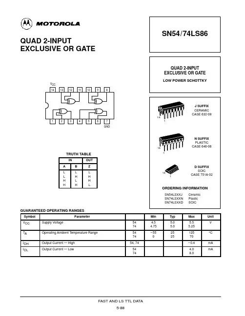
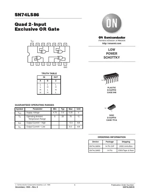
SN54/74LS86 QUAD 2-INPUT EXCLUSIVE OR GATE
QUAD 2-INPUT EXCLUSIVE OR GATE
LOW POWER SCHOTTKY
VCC 14 13 12 11 10 9 8
J SUFFIX CERAMIC CASE 632-08
GUARANTEED OPERATING RANGES
Symbol VCC TA IOH IOL Supply Voltage Operating Ambient Temperature Range Output Current — High Output Current — Low Parameter 54 74 54 74 54, 74 54 74 Min 4.5 4.75 – 55 0 Typ 5.0 5.0 25 25 Max 5.5 5.25 125 70 – 0.4 4.0 8.0 Unit V °C mA mA
FAST AND LS TTL DATA 5-89
14
1
2
3
4
6
7 GND
1
14
N SUFFIX PLASTIC CASE 646-06
1
TRUTH TABLE
IN A L L H H B L H L H OUT Z L H H L
14 1
D SUFFIX SOIC CASE 751A-02
ORDERING INFORMATION
SN54LSXXJ SN74LSXXN SN74LSXXD Ceramic Plastic SOIC
VCC = MAX, VIN = 2.7 V VCC = MAX, VIN = 7.0 V VCC = MAX, VIN = 0.4 V VCC = MAX VCC = MAX
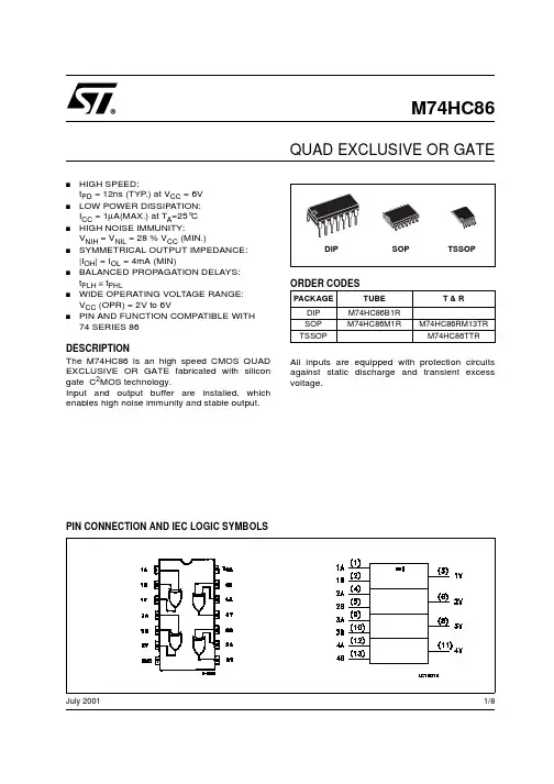
ST M74HC86 数据手册
1/8July 2001sHIGH SPEED:t PD = 12ns (TYP .) at V CC = 6V sLOW POWER DISSIPATION:I CC = 1µA(MAX.) at T A =25°C sHIGH NOISE IMMUNITY:V NIH = V NIL = 28 % V CC (MIN.)sSYMMETRICAL OUTPUT IMPEDANCE:|I OH | = I OL = 4mA (MIN)sBALANCED PROPAGATION DELAYS:t PLH ≅ t PHLsWIDE OPERATING VOLTAGE RANGE:V CC (OPR) = 2V to 6VsPIN AND FUNCTION COMPATIBLE WITH 74 SERIES 86DESCRIPTIONThe M74HC86 is an high speed CMOS QUAD EXCLUSIVE OR GATE fabricated with silicon gate C 2MOS technology.Input and output buffer are installed, which enables high noise immunity and stable output.All inputs are equipped with protection circuits against static discharge and transient excess voltage.M74HC86QUAD EXCLUSIVE OR GATEPIN CONNECTION AND IEC LOGIC SYMBOLSORDER CODESPACKAGE TUBE T & R DIP M74HC86B1R SOP M74HC86M1RM74HC86RM13TR TSSOPM74HC86TTRM74HC862/8INPUT AND OUTPUT EQUIVALENT CIRCUITPIN DESCRIPTIONTRUTH TABLEABSOLUTE MAXIMUM RATINGSAbsolute Maximum Ratings are those values beyond which damage to the device may occur. Functional operation under these conditions is not implied(*) 500mW at 65 °C; derate to 300mW by 10mW/°C from 65°C to 85°CRECOMMENDED OPERATING CONDITIONSPIN No SYMBOL NAME AND FUNCTION 1, 4, 9, 121A to 4A Data Inputs 2, 5, 10, 131B to 4B Data Inputs 3, 6, 8, 111Y to 4Y Data Outputs 7GND Ground (0V)14V CCPositive Supply VoltageA B Y L L L L H H H L H HHLSymbol ParameterValue Unit V CC Supply Voltage -0.5 to +7V V I DC Input Voltage -0.5 to V CC + 0.5V V O DC Output Voltage -0.5 to V CC + 0.5V I IK DC Input Diode Current ± 20mA I OK DC Output Diode Current ± 20mA I ODC Output Current± 25mA I CC or I GND DC V CC or Ground Current± 50mA P D Power Dissipation500(*)mW T stg Storage Temperature -65 to +150°C T LLead Temperature (10 sec)300°CSymbol ParameterValue Unit V CC Supply Voltage 2 to 6V V I Input Voltage 0 to V CC V V O Output Voltage 0 to V CC V T op Operating Temperature -55 to 125°C t r , t fInput Rise and Fall TimeV CC = 2.0V 0 to 1000ns V CC = 4.5V 0 to 500ns V CC = 6.0V0 to 400nsM74HC863/8DC SPECIFICATIONSAC ELECTRICAL CHARACTERISTICS (C L = 50 pF, Input t r = t f = 6ns)CAPACITIVE CHARACTERISTICS1) C PD is defined as the value of the IC’s internal equivalent capacitance which is calculated from the operating current consumption without load. (Refer to Test Circuit). Average operating current can be obtained by the following equation. I CC(opr) = C PD x V CC x f IN + I CC /4 (per gate)SymbolParameterTest ConditionValue UnitV CC (V)T A = 25°C -40 to 85°C -55 to 125°C Min.Typ.Max.Min.Max.Min.Max.V IHHigh Level Input Voltage2.0 1.5 1.5 1.5V 4.53.15 3.15 3.156.04.24.24.2V ILLow Level Input Voltage2.00.50.50.5V4.5 1.35 1.35 1.356.0 1.81.81.8V OHHigh Level Output Voltage2.0I O =-20 µA 1.9 2.0 1.9 1.9V4.5I O =-20 µA 4.4 4.5 4.4 4.46.0I O =-20 µA5.96.0 5.9 5.94.5I O =-4.0 mA 4.18 4.31 4.13 4.106.0I O =-5.2 mA 5.685.8 5.635.60V OLLow Level Output Voltage2.0I O =20 µA 0.00.10.10.1V 4.5I O =20 µA 0.00.10.10.16.0I O =20 µA 0.00.10.10.14.5I O =4.0 mA 0.170.260.330.406.0I O =5.2 mA 0.180.260.330.40I I Input Leakage Current6.0V I = V CC or GND ± 0.1± 1± 1µA I CCQuiescent Supply Current6.0V I = V CC or GND11020µA SymbolParameterTest ConditionValue UnitV CC (V)T A = 25°C -40 to 85°C -55 to 125°C Min.Typ.Max.Min.Max.Min.Max.t TLH t THL Output TransitionTime 2.0307595110ns 4.581519226.07131619t PLH t PHL Propagation DelayTime2.0561********ns4.5142228336.012192428SymbolParameterTest ConditionValue UnitV CC (V)T A = 25°C -40 to 85°C -55 to 125°C Min.Typ.Max.Min.Max.Min.Max.C IN Input Capacitance 5.05101010pF C PDPower Dissipation Capacitance (note 1)5.026pFM74HC864/8TEST CIRCUITL R T = Z OUT of pulse generator (typically 50Ω)WAVEFORM : PROPAGATION DELAY TIME(f=1MHz; 50% duty cycle)M74HC86Information furnished is believed to be accurate and reliable. However, STMicroelectronics assumes no responsibility for the consequences of use of such information nor for any infringement of patents or other rights of third parties which may result from its use. No license is granted by implication or otherwise under any patent or patent rights of STMicroelectronics. Specifications mentioned in this publication are subject to change without notice. This publication supersedes and replaces all information previously supplied. STMicroelectronics products are not authorized for use as critical components in life support devices or systems without express written approval of STMicroelectronics.© The ST logo is a registered trademark of STMicroelectronics© 2001 STMicroelectronics - Printed in Italy - All Rights ReservedSTMicroelectronics GROUP OF COMPANIESAustralia - Brazil - China - Finland - France - Germany - Hong Kong - India - Italy - Japan - Malaysia - Malta - MoroccoSingapore - Spain - Sweden - Switzerland - United Kingdom© 8/8。
74系列芯片型号、参数介绍
74系列芯⽚型号、参数介绍74HC/LS/HCT/F系列芯⽚的区别1、 LS是低功耗肖特基,HC是⾼速COMS。
LS的速度⽐HC略快。
HCT输⼊输出与LS兼容,但是功耗低;F是⾼速肖特基电路;2、 LS是TTL电平,HC是COMS电平。
3、 LS输⼊开路为⾼电平,HC输⼊不允许开路, hc ⼀般都要求有上下拉电阻来确定输⼊端⽆效时的电平。
LS 却没有这个要求4、 LS输出下拉强上拉弱,HC上拉下拉相同。
5、⼯作电压不同,LS只能⽤5V,⽽HC⼀般为2V到6V;6、电平不同。
LS是TTL电平,其低电平和⾼电平分别为0.8和V2.4,⽽CMOS在⼯作电压为5V时分别为0.3V和3.6V,所以CMOS可以驱动TTL,但反过来是不⾏的7、驱动能⼒不同,LS⼀般⾼电平的驱动能⼒为5mA,低电平为20mA;⽽CMOS的⾼低电平均为5mA;8、 CMOS器件抗静电能⼒差,易发⽣栓锁问题,所以CMOS的输⼊脚不能直接接电源。
74系列集成电路⼤致可分为6⼤类:. 74××(标准型);.74LS××(低功耗肖特基);.74S××(肖特基);.74ALS××(先进低功耗肖特基);.74AS××(先进肖特基);.74F××(⾼速)。
近年来还出现了⾼速CMOS电路的74系列,该系列可分为3⼤类:. HC为COMS⼯作电平;. HCT为TTL⼯作电平,可与74LS系列互换使⽤;.HCU适⽤于⽆缓冲级的CMOS电路。
这9种74系列产品,只要后边的标号相同,其逻辑功能和管脚排列就相同。
根据不同的条件和要求可选择不同类型的74系列产品,⽐如电路的供电电压为3V就应选择74HC系列的产品系列电平典型传输延迟ns 最⼤驱动电流(-Ioh/Lol)mAAHC CMOS 8.5 -8/8AHCT COMS/TTL 8.5 -8/8HC COMS 25 -8/8HCT COMS/TTL 25 -8/8ACT COMS/TTL 10 -24/24F TTL 6.5 -15/64ALS TTL 10 -15/64LS TTL 18 -15/24LVCACSLC注:同型号的74系列、74HC系列、74LS系列芯⽚,逻辑功能上是⼀样的。
74系列芯片功能介绍
74LS112A 74F112、74ALS112 74S112、74HC112双J-K负沿触发器
(带预置和清除端)
功能表
74LS113A 74S113 74F113、74ALS113 74HC113双J-K负沿触发器
(带预置)
功能表
74LS114A 74F114 74ALS114 74F114 74HC114双J-K负沿触发器
端)
功能表
7480门输入全加器
功能表
7482 2位二进制全加器
执行两个2位二进制的加法,每一位都有和(艺)输出,由第二位产
生最后的进位(C2)。
功能表
7483A、74LS83A、74HC83、74C834位二进制全加器(带超前进位) 功能表
执行两个4位二进制数加法,每位有一个和(艺)输出,最后的进位
74C20双四输入与非门
Y=/ABCD
7421、74F21、74ALS21、74LS21、74HC21双四输入与门
Y=ABCD
7422、74H22 74LS22、74S22、74ALS22 74HC22双四输入与非 门(OC
Y二/ABCD是74XX20的集电极开路型。
7423可扩展双4输入或非门(带选通端)
复位/计数功能表7491A、74L91、74LS91、74HC918位移位寄存器
7492A、74LS92、74HC92十二分频计数器 二分频和六分频;有复位输入。
7493A、74L93、74LS93、74HC93、74C934位二进制计数器 二分频和六分频;有复位输入。
功能表
7494 4位寄存器 执行右移操作,用作串入串出寄存器或双源并串转换器。 预置功能表(位A,所有的典型)7495A、74LS95B、74HC95、74C954位并行存取移位寄存器 具有并行和串行输入、 并行输出、 模式控制和二个时钟输入; 有三种 运算方式,并行写入、右移(方向从QA向QD、左移(方向从QD向QA)。
SN74LS86中文资料
LOW POWER SCHOTTKYDevice Package Shipping SN74LS86N 14 Pin DIP 2000 Units/Box SN74LS86D14 PinSOIC D SUFFIX CASE 751A2500/T ape & ReelPLASTIC N SUFFIX CASE 646141141ON Semiconductor and are trademarks of Semiconductor Components Industries, LLC (SCILLC). SCILLC reserves the right to make changes without further notice to any products herein. SCILLC makes no warranty, representation or guarantee regarding the suitability of its products for any particular purpose, nor does SCILLC assume any liability arising out of the application or use of any product or circuit, and specifically disclaims any and all liability, including without limitation special, consequential or incidental damages. “Typical” parameters which may be provided in SCILLC data sheets and/or specifications can and do vary in different applications and actual performance may vary over time. All operating parameters, including “Typicals” must be validated for each customer application by customer’s technical experts. SCILLC does not convey any license under its patent rights nor the rights of others.SCILLC products are not designed, intended, or authorized for use as components in systems intended for surgical implant into the body, or other applications intended to support or sustain life, or for any other application in which the failure of the SCILLC product could create a situation where personal injury or death may occur. Should Buyer purchase or use SCILLC products for any such unintended or unauthorized application, Buyer shall indemnify and hold SCILLC and its officers, employees, subsidiaries, affiliates, and distributors harmless against all claims, costs, damages, and expenses, and reasonable attorney fees arising out of, directly or indirectly, any claim of personal injury or death associated with such unintended or unauthorized use, even if such claim alleges that SCILLC was negligent regarding the design or manufacture of the part. SCILLC is an Equal Opportunity/Affirmative Action Employer. PUBLICATION ORDERING INFORMATIONASIA/PACIFIC: LDC for ON Semiconductor – Asia SupportPhone:303–675–2121 (Tue–Fri 9:00am to 1:00pm, Hong Kong Time)Toll Free from Hong Kong 800–4422–3781Email: ONlit–asia@JAPAN: ON Semiconductor, Japan Customer Focus Center4–32–1 Nishi–Gotanda, Shinagawa–ku, Tokyo, Japan 141–8549Phone: 81–3–5487–8345Email: r14153@Fax Response Line:303–675–2167。
74ls74中文资料
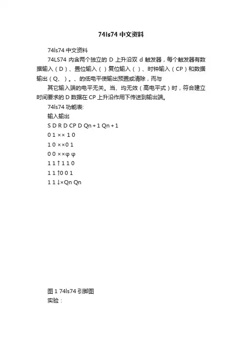
74ls74中文资料74ls74中文资料74LS74内含两个独立的D上升沿双d触发器,每个触发器有数据输入(D)、置位输入()复位输入()、时钟输入(CP)和数据输出(Q、)。
、的低电平使输出预置或清除,而与其它输入端的电平无关。
当、均无效(高电平式)时,符合建立时间要求的D数据在CP上升沿作用下传送到输出端。
74ls74功能表:输入输出S D R D CP D Qn+1 Qn+10 1 ×× 1 01 0 ××0 10 0 ××φ φ1 1 ↑ 1 1 01 1 ↑0 0 11 1 ↓×Qn Qn图1 74ls74引脚图实验:用74LS74构成4位寄存器一个D触发器可实现一位二进数的存储,因此应采用4个D触发器实现4位寄存器。
由于要实现移位寄存,4个D触发器之间应相互联接。
(1)首先在图2中完成相应的联线,构成可实现并入并出、串入串出、并入串出、串入并出的多功能移位寄存。
按图接好电路。
(2) D3 D2 D1 D0分别接逻辑开关,Q3 Q2 Q1 Q0接发光二极管;(3) 先清零;(4) 按下列要求,实现相应功能,观察结果,并描述工作过程。
并入并出:使数据输入端D3D2D1D0=1011,给CP端输入一个正单脉冲,观察Q3Q2Q1Q0发光二极管的状态,、将结果填入表中。
并入串出:使数据输入端D3D2D1D0=1011,给CP端输入4个正单脉冲,观察Q3端发光二极管的状态,将结果填入表6中。
串入并出:使数据输入端D0分别为1011,同时通过给CP端输入正单脉冲将D0端的4 个数据送入寄存器。
观察Q3Q2Q1Q0端发光二极管的状态,将结果填入表中。
串入串出:使数据输入端D0分别为1011,同时通过给CP端输入正单脉冲,将D0端的4 个数据送入寄存器。
在CP端输完8个脉冲后,观察Q3端发光二极管的状态,将结果填入表2中。
并入并出:D3D2D1D0=10111个CP脉冲Q3Q2Q1Q0=结论:并入串出D3D2D1D0=10114个CP脉冲Q3=结论串入并出D3=10114个CP脉冲Q3Q2Q1Q0=结论串入串出D3=10118个CP脉冲Q3=结论图274ls153芯片管脚图引脚逻辑功能以及封装2007年12月17日 23:53 本站原创作者:本站用户评论()关键字:74ls153管脚图逻辑功能图封装:74LS163引脚功能表及管脚定义图(带时序波形图)发布:2011-08-30 | 作者: | 来源: huangjiapeng| 查看:2620次 | 用户关注:定时器由与系统秒脉冲(由时钟脉冲产生器提供)同步的计数器构成,要求计数器在状态信号ST作用下,首先清零,然后在时钟脉冲上升沿作用下,计数器从零开始进行增1计数,向控制器提供模5的定时信号TY和模25的定时信号TL。
74LV86BQ资料
Rev. 03 — 27 November 2007
© NXP B.V. 2007. All rights reserved.
3 of 15
元器件交易网
NXP Semiconductors
74LV86
Quad 2-input exclusive-OR gate
9. Static characteristics
Table 6. Static characteristics Voltages are referenced to GND (ground = 0 V).
74LV86PW
−40 °C to +125 °C TSSOP14 plastic thin shrink small outline package; 14 leads; body width 4.4 mm
74LV86BQ
−40 °C to +125 °C
DHVQFN14 plastic dual in-line compatible thermal enhanced very thin quad flat package; no leads; 14 terminals; body 2.5 × 3 × 0.85 mm
元器件交易网
74LV86
Quad 2-input exclusive-OR gate
Rev. 03 — 27 November 2007
Product data sheet
1. General description
The 74LV86 is a low-voltage Si-gate CMOS device that is pin and function compatible with 74HC86 and 74HCT86. The 74LV86 provides a quad 2-input exclusive-OR function.
74LS08中文资料
54/7408四2输入与门简要说明08为四组2输入端与门(正逻辑),共有54/7408、54/74S08、54/74LS08三种线路结构型式,其主要电特性的典型值如下:型号t PLHt phlP D54/7408 17.5ns 12ns 78mW 54/74S08 4.5ns 5ns 125mW 54/74LS08 8ns 10ns 17mW引出端符号1A -4A 输入端 1B -4B 输入端 1Y -4Y 输出端逻辑图双列直插封装极限值电源电压 …………………………………………. 7V 输入电压54/7408、54/74S08………………………………. 5.5V 54/74LS08 ………………………………………. 7V A -B 间电压54/7408、54/74S08..................................... 5.5V 输出截止态电压. (7V)h tt p ://w ww .e l e c f a ns .c om工作环境温度 54XXX ……………………………………………. -55~125℃ 74XXX………… ……………………………… 0~70℃ 存储温度 …………………………………………. -65~150℃功能表:推荐工作条件:5408/7408 54S08/74S08 54LS08/74LS08 最小 额定 最大 最小额定最大 最小额定 最大单位54 4.5 5 5.5 4.5 5 5.5 4.5 5 5.5 电源电压VCC 74 4.75 5 5.25 4.75 5 5.25 4.75 5 5.25V 输入高电平电压V iH2 2 2 V 540.8 0.8 0.7 输入低电平电压V iL74 0.8 0.8 0.8 V 输出高电平电流I OH -800 -1000 -400 µA5416 20 4 输出低电平电流I OL74 16 20 8 mA静态特性(TA 为工作环境温度范围)‘08 ‘S08 ‘LS08 参 数测 试 条 件【1】最小最大最小最大最小 最大单位I ik =-12mA -1.5 V IK 输入嵌位电压 Vcc=最小I ik =-18mA-1.2 -1.5 V54 2.4 2.5 2.5 V OH 输出高电平电压 Vcc =最小V IH =2V ,I OH =最大74 2.4 2.7 2.7 V 54 0.4 0.5 0.4 V OL 输出低电平电压 Vcc=最小,V IL =最大,I OL =最大74 0.4 0.5 0.5 V V I =5.5V 1 1 I I 最大输入电压时输入电流Vcc =最大 V I =7V 0.1 mA V IH =2.4V 40 I IH 输入高电平电流 Vcc =最大V IH =2.7V 50 20µAV IL =0.4V -1.6 -0.4I IL 输入低电平电流 Vcc =最大V IL =0.5V -2mA 54 -20 -55 -40 -100-20 -100I OS 输出短路电流 Vcc =最大74 -18 -55 -40 -100-20 -100mA I CCH 输出高电平时电源电流 Vcc =最大21 32 4.8 mA I CCL 输出低电平时电源电流 Vcc =最大33 57 8.8 mA[1]: 测试条件中的“最小”和“最大”用推荐工作条件中的相应值。
74LS90中文资料参数
功能表
复位输入
复位/计数功能表
输
出
R0(1)
R0(2)
R9(1)
R9(2)
QD
QC
QB
QA
H
H
L
×
L
L
L
L
H
H
×
L
L
L
L
L
×
×
H
H
H
L
L
H
×
L
×
L
计数(COUNT)
L
×
L
×
计数(COUNT)
L
×
×
L
计数(COUNT)
×
L
L
×
计数(COUNT)
H=高电平 L=低电平 ×=不定
天水天光半导体有限责任公司(八七一厂) 2005.1 版
对于52进制计数输出qd连到输入a计数推荐工作条件推荐工作条件74参数值最小典型4752000153015254054参数值最小典型最大45520400001530152555符号参数名称最大525084008321685单位vccvihviliohiol电源电压输入高电平电压输入低电平电压输出高电平电流输出低电平电流55507vvvama43216125a输入b输入a输入b输入复位输入fck时钟频率mhztw脉冲宽度nsthta复位无效态保持时间工作环境温度ns天水天光半导体有限责任公司八七一厂20051版天水天光半导体有限责任公司八七一厂20051版54ls9074ls90lsttl型十进制计数器2和554ls9074ls90lsttl型十进制计数器2和5电性能
典型参数: f 工作频率=42MHz Pd=45mW
外引线排列图
74LS74中文资料_数据手册_参数
74LS74双正边沿触发的D触发器预设清除和补充输出一般描述该器件包含两个独立74LS74的正边沿触发器,带互补输出的带触发器 的D触发器INFORMA- D输入端上的触发器接受位置上的触发器,时钟脉冲前沿触发发生在A电压电平并且与转换时间不直接相关 时钟上升沿的数据可能是D输入端的数据在不影响时钟低或高时更改只要数据建立和保持时间不相等,输出就可以违反预置或清除 输入的低逻辑电平无论逻辑电平如何,设置或复位输出其他投入特征 ?备用军用太空装置(74LS74)能联系美国国家半导体销售办 事处分销商的规格连接图双列直插式封装 TLF6373 - 1订单号54LS74DMQB 54LS74FMQB 54LS74LMQB DM54LS74AJ DM54LS74AW DM74LS74AM或DM74LS74AN参见NS包装号E20A J14A M14A N14A或W14B功能表输入输出 PR CLR CLK D Q Q LH X X H大号 HL X X大号 H二 X X H H HH ü HH大号 HH ü二 H HH大号 X Q 0 Q 0 高逻辑电平 X E 低或高逻辑电平 低逻辑电平 你是 积极的过渡 ?这 种配置是不稳定的,即当预置时它不会持续并且清除输入返回到其非活动(高)级别 Q 0 E 在74LS74指示的输入条件建立之前,Q 的输出逻辑电平 C1995美国国家半
- 1、下载文档前请自行甄别文档内容的完整性,平台不提供额外的编辑、内容补充、找答案等附加服务。
- 2、"仅部分预览"的文档,不可在线预览部分如存在完整性等问题,可反馈申请退款(可完整预览的文档不适用该条件!)。
- 3、如文档侵犯您的权益,请联系客服反馈,我们会尽快为您处理(人工客服工作时间:9:00-18:30)。
Singapore 049318
Harbour City, Canton Road, Tsim Sha Tsui,
Tel: 535-2100
Kowloon, Hong Kong
Fax: 535-1533
Tel: <852> (2) 735 9218
Fax: <852> (2) 730 0281
Hitachi Asia Ltd.
Hitachi Europe GmbH Electronic components Group Dornacher Stra§e 3 D-85622 Feldkirchen, Munich Germany Tel: <49> (89) 9 9180-0 Fax: <49> (89) 9 29 30 00
DP-14 Conforms Conforms 0.97 g
10.06 10.5 Max
14
8
5.5
1
7
1.42 Max
0.10 ± 0.10
1.27
*0.42 ± 0.08 0.40 ± 0.06
0.15 0.12 M
*Dimension including the plating thickness Base material dimension
For further information write to:
Hitachi Semiconductor (America) Inc. 179 East Tasman Drive, San Jose,CA 95134 Tel: <1> (408) 433-1990 Fax: <1>(408) 433-0223
Hitachi Europe Ltd. Electronic Components Group. Whitebrook Park Lower Cookham Road Maidenhead Berkshire SL6 8YA, United Kingdom Tel: <44> (1628) 585000 Fax: <44&g& Integrated Circuits.
Nippon Bldg., 2-6-2, Ohte-machi, Chiyoda-ku, Tokyo 100-0004, Japan
Tel: Tokyo (03) 3270-2111 Fax: (03) 3270-5109
URL
Hitachi Asia Pte. Ltd.
Hitachi Asia (Hong Kong) Ltd.
16 Collyer Quay #20-00
Group III (Electronic Components)
Hitachi Tower
7/F., North Tower, World Finance Centre,
2. Products and product specifications may be subject to change without notice. Confirm that you have received the latest product standards or specifications before final design, purchase or use.
written approval from Hitachi. 7. Contact Hitachi’s sales office for any questions regarding this document or Hitachi semiconductor
products.
Hitachi, Ltd.
3. Hitachi makes every attempt to ensure that its products are of high quality and reliability. However, contact Hitachi’s sales office before using the product in an application that demands especially high quality and reliability or where its failure or malfunction may directly threaten human life or cause risk of bodily injury, such as aerospace, aeronautics, nuclear power, combustion control, transportation, traffic, safety equipment or medical equipment for life support.
19.20 20.32 Max
14
8
1
1.30 7
2.39 Max
6.30 7.40 Max
Unit: mm 7.62
0.51 Min 2.54 Min 5.06 Max
2.54 ± 0.25
0.48 ± 0.10
0.25
+ –
0.10 0.05
0° – 15°
Hitachi Code JEDEC EIAJ Weight (reference value)
NorthAmerica Europe Asia (Singapore) Asia (Taiwan) Asia (HongKong) Japan
: http:/ : /hel/ecg : .sg/grp3/sicd/index.htm : /E/Product/SICD_Frame.htm : /eng/bo/grp3/index.htm : http://www.hitachi.co.jp/Sicd/indx.htm
0° – 8°
Hitachi Code JEDEC EIAJ Weight (reference value)
FP-14DN Conforms Conforms 0.13 g
Cautions
1. Hitachi neither warrants nor grants licenses of any rights of Hitachi’s or any third party’s patent, copyright, trademark, or other intellectual property rights for information contained in this document. Hitachi bears no responsibility for problems that may arise with third party’s rights, including intellectual property rights, in connection with use of the information contained in this document.
4. Design your application so that the product is used within the ranges guaranteed by Hitachi particularly for maximum rating, operating supply voltage range, heat radiation characteristics, installation conditions and other characteristics. Hitachi bears no responsibility for failure or damage when used beyond the guaranteed ranges. Even within the guaranteed ranges, consider normally foreseeable failure rates or failure modes in semiconductor devices and employ systemic measures such as failsafes, so that the equipment incorporating Hitachi product does not cause bodily injury, fire or other consequential damage due to operation of the Hitachi product.
2.20 Max
*0.22 ± 0.05 0.20 ± 0.04
Unit: mm
7.80
+ –
0.20 0.30
1.15
0.70 ± 0.20
0° – 8°
Hitachi Code JEDEC EIAJ Weight (reference value)
FP-14DA — Conforms 0.23 g
Copyright ' Hitachi, Ltd., 1999. All rights reserved. Printed in Japan.
万联芯城电子元器件物料专供终端研发生产企业,只售原 装正品,万联芯城电子元器件物料均来自原厂及授权代理 商,目录分销商,保证货源渠道优质,价格优势明显,可 进行一站式配单,电子元器件一站式采购可为客户省去逐 个查找环节,只需提供 BOM 表,即可为您报价,万联芯城 电子元器件配单服务可以为客户节省采购成本,满足客户 物料需求,丰富的电子元器件供应链体系已为全国多家终 端企业服务,点击进入万联芯城。