TD2072限幅放大器和激光驱动器的收发器_CN
ALU 产品手册

上海贝尔行业产品手册公司介绍阿尔卡特朗讯是全球领先的通信解决方案供应商,专注于IP网络、超宽带接入和云技术,致力于为全球的运营商、企业和政府机构提供更加灵活、快速、可靠的通信网络。
阿尔卡特朗讯旗下的贝尔实验室是全球最具活力的前沿技术研究机构之一,贡献了一大批奠定现代信息通信基础的创新发明。
贝尔实验室共获得8项诺贝尔奖,拥有14位诺贝尔奖获得者。
最近,阿尔卡特朗讯凭借一系列技术创新,获得国际机构的高度认可。
上海贝尔股份有限公司成立于1984年,是国务院国有资产监督管理委员会的直属企业,也是中国第一家外商投资股份制公司,拥有强大的本土实力和广泛的全球资源。
上海贝尔为运营商、企业和行业客户提供先进的信息通信解决方案和高质量的服务,其产品覆盖有线和无线方案、IP网络、光网络、光接入、云计算、网络核心及应用、网络管理及服务等诸多领域。
上海贝尔拥有贝尔实验室中国研究中心和数个重要的全球研发中心,可全面进入阿尔卡特朗讯全球技术库,开发服务于中国和阿尔卡特朗讯全球客户的独创技术,并且在多项新技术开发中居于主导地位。
上海贝尔拥有技术先进、制造能力达到世界一流水平的生产制造平台,公司销售服务网络遍及全国和海外50多个国家。
今天,上海贝尔已成为集世界一流的生产制造基地,全球重要的研发中心、采购和物流中心、信息服务中心以及上海贝尔大学于一体的阿尔卡特朗讯在全球的旗舰。
目录总体描述 (4)行业解决方案 (5)全业务传送网解决方案 (5)城域网解决方案 (8)骨干网解决方案 (9)数据中心网络解决方案 (10)数据中心互联/出口解决方案 (11)电力数据调度网与综合数据网解决方案 (12)专业DNS_DHCP_IPAM系统解决方案 (13)无源局域网解决方案(POL) (15)端到端L TE解决方案 (17)IMS/NGN解决方案 (19)产品系列 (21)光传送 (21)OTN/WDM 产品-1830 PSS系列产品 (21)PTN-1850 TSS系列产品 (23)MSTP系列产品 (24)微波传输 (25)中短距分组微波-9500 MPR系列产品 (25)长距微波-9600 LSY系列产品 (26)数据承载 (27)骨干/核心路由平台-7950 XRS (27)城域业务路由-7750 SR/7705 SAR (28)MES系列交换机 (30)软件定义网络– Nuage SDN (32)VitalQIP:面向IPv4、IPv6的下一代IP地址管理解决方案 (33)超宽带接入 (34)PON OL T局端设备-7360 ISAM FX (34)丰富的光终端(ONU)系列 (34)LTE无线产品 (37)业务核心网 (38)IMS产品 (38)NGN产品 (38)总体描述通信网的未来将会何去何从?企业期望应对动态的市场和客户需求,实施新的业务策略并开拓新的市场机会,今天的网络已经无法应对日益增长的海量数据,我们需要一个灵活敏捷、伸缩自如的人性化网络,基于IP的网络演进势在必行,而这一切必须以网络为基石。
夏普光耦选型手册
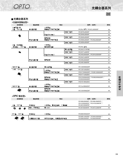
4脚 DIP
PC815XNNSZ0F*5, *6 复 合 光 晶 PC81510NSZ0X 体 管 5, 6 输 PC852XNNSZ0F* * 出 PC853XNNSZ0F*5, *6
*1 *2 *3 *4 *5 *6 *7 *8 *9
–
–
50
5.0
35
600
1
60
100
⅜ ⅜ ⅜
– ⅜ ⅜
–
10
页码 40 40 40 40 40 40 41 41 41 41 41 41 41 42 42 42 42 42 42 43 43
<OPIC 输出型>
封装类型 输出类型 特点 型号 (系列) PC400J00000F/PC456L0NIP0F/ PC410S0NIP0F /PC410L0NIP0F / PC4D10SNIP0F PC457S0NIP0F /PC457L0NIP0F 页码
PC714V0NSZXF PC724V0NSZXF
高绝缘电压 高绝缘电压, 大输入电流 高绝缘电压, 带基底端子 高绝缘电压, 高灵敏度 高绝缘电压, 高灵敏度, 高集电极发射极电压, 大功率
PC3HU7xYIP0B
PC3H2J00000F (小扁平型4脚)
注意: 未经元器件规格说明书确认,便在设备中使用产品目录、数据手册等所刊载的任何夏普元器件,由此引起的故障或损害,夏普公 司将不负任何责任。 除非特别说明,本页所列的型号均符合 RoHS (有害物质限制)标准* 。详情请与夏普公司联系。 *RoHS (有害物质限制)标准:禁止使用铅、镉、六价铬、汞和特定溴系阻燃剂 (PBB 和 PBDE) ,除特别情况外。 因此,在使用任何夏普元器件之前,务请与夏普公司联系以获取最新的元器件规格说明书。
安装指南- extron fox3 sr 201 光纤缩放接收器说明书

1I M P O .e x t r o n .c o m f o r t i o ni n s t r u c ti on s ,e c t i n g t h eFOX3 SR 201 • Setup GuideThis guide provides quick start instructions for an experienced installer to set up and operate the Extron FOX3 SR 201 Fiber Opticscaling receivers. This scaling receiver scales resolutions up to 4K @ 60 Hz, 4:4:4 video, and extends with 2-CH audio, RS-232, and IR over fiber. The FOX3 SR 201 is available in either singlemode (SM) or multimode (MM) transmission mode.InstallationREMOTEPOWER 12V2.0A MAXA OUT IN BOUT INLANHDMIFOX3 SR 201RAUDIOCONTROLOUTPUTSIG F C A D H E BFigure 1.FOX3 SR 201 Rear PanelA Power Inlet F Remote RS-232B Power LED G LAN Ethernet portC Audio output H SFP module and LEDsD HDMI output I Reset buttonE Control RS-232/IR portStep 1 — MountingTurn off or disconnect all equipment power sources and mount the scaling receiver as required. For mounting details and considerations, see the FOX3 SR 201 User Guide at .Step 2 — Output Connectionsa. D ).b. C ) (see figure 2 to wire the captive screwUnbalanced Stereo OutputBalanced Stereo Output LRLRa. To pass serial, IR data, or control signals, such as for serial control of a projector,connect the master device to the transmitter and the controlled device to thereceiver via the CONTROL 5-pole captive screw connector (see E and figure 3 for wiring).Figure 3. RS-232 and IR Wiring2FOX3 SR 201 • Setup Guide (Continued)b. For remote control of a unit and loading firmware (LAN or USB only), connect a host device, such as a computer or controlsystem, to one of the following ports (see the FOX3 SR 201 User Guide , available at , for details):•Remote RS-232 port — Connect the 3-pole captive screw connector to this port (F ). The protocol for the Remote port is as follows:• 9600 baud • no parity • 8 data bits • 1 stop bit • no flow control• LAN Ethernet port — Connect an RJ-45 connector to this port (G ).•USB Configuration port — Connect a USB mini-B connector to this port (see figure 5, B on page 2).Step 4 — Throughput Connections).b. to the transmitter, connect a cable between the A Out port on the receiver and A In port on the transmitter (2).c. To transmit an uncompressed 4K @ 60 Hz signal, using the Uncompressed Video LinkLicense,repeat step 4a on the SFP B port on the scaling receiver SFP Link LEDs — ReceiverFigure 4.Fiber Cable Connection• Transmit Optical OUT LED — Lights solid green when powered and lights off when there is no power on the endpoint.•Receive Optical IN LED — Lights solid green when light is present and lights off when there is no power or light present.Step 5 — Power ConnectionConnect the included external 12 VDC power supply into the 2-pole connector (see figure 1, A on page 1). The power LED lights (B ) when the unit is receiving power.OperationAfter the receiver, transmitter, and their connected devices are powered up, the system is fully operational. If any problems are encountered, verify that the cables are routed and connected properly and the display device has a compatible resolution and refresh rate. If problems persist, call the Extron S3 Sales & Technical Support Hotline (see the contact number on page 6).FOX3 SR 201MENUINPUTSIGNAL HDCPENTER C AD EB Figure 5.FOX3 SR 201 Front PanelA Power LED — Indicates power is applied to the unit.B USB Config port — Connect a USB Mini-B cable to a computer to configure the device and update the firmware via ProductConfiguration Software (PCS), Simple Instruction Set (SIS) commands, or internal web pages.C Input LEDs —• Signal LED — Lights when the unit detects an input video signal.•HDCP LED — Lights when the input signal is HDCP encrypted.D Menu and Enter buttons — Press these buttons to access and navigate the on-screen display menu system.E Navigation buttons — Press these buttons to navigate through the on-screen display menu system or change settings. ResetPress the rear panel recessed reset button (see figure 1, I on page 1) if the FOX3 scaling receiver firmware is corruptedor the unit gets disconnected during the update process. The different resets allow the device to revert to the factory loaded firmware, reset IP seetings, or reset configuration to default (see the Reset Modes table, for details on the reset modes).Front Panel Lockout Mode (Executive Mode)The front panel lockout mode limits operation of the device from the front panel. When enabled, use SIS commands or the Product Configuration Software (PCS) to configure the device. To enable or disable the front panel lockout mode through the front panel, press and hold the Menu (see figure 5, D on page 2) and down arrow (E) buttons simultaneously for 5 seconds oruntil the power LED blinks.34FOX3 SR 201 • Setup Guide (Continued)Configuration and ControlTo configure the FOX3 SR, use the front panel controls and the on-screen display (OSD) menu, Simple instruction Set (SIS) commands, or PCS.On-screen display menu systemThe OSD menu consists of two submenus, Device Info and Setup , that can be accessed using the front panel Menu button. View the menu on a display connected to the HDMI output connector (see figure 1, D on page 2). The Device Info submenu is view only. The following fields can be configured from the Setup submenu:•Output Rate — Select from a list of refresh rates (see Output Resolution table on page 5). The default setting is 1080p @ 60 Hz.•HDMI Format — Select the output format:• Auto (default)• DVI RGB 444• HDMI RGB 444 Full • HDMI RGB 444 Limited • HDMI YUV 444 Full • HDMI YUV 444 Limited • HDMI YUV 422 Full •HDMI YUV 422 Limited• Test Pattern — Select an available test pattern to display or turn a test pattern off. The available test pattern selections are Crop, Alternating Pixels, Crosshatch, and Color Bars. The default setting is Off.•Factory Reset — Reset the unit to its factory default values (removing any user-specified values) while retaining all TCP/IP settings.To adjust settings:1. Press the Menu button to access the main menu.2. Press the directional arrows to navigate to a desired submenu.3. Press the Enter button to access submenu items of a selected submenu.4. Press the directional arrows to navigate a desired submenu item.5. Press the Enter button to select a submenu item for adjustment.6. As required, press the directional arrows or press the Enter button to adjust submenu items.7. Press the Menu button to return to the list of submenus or exit the OSD menu.Product Configuration SoftwareThe FOX3 scaling receiver can be configured via the Product Configuration Software when it is installed on a connected host device, such as a PC, through the front panel USB port or LAN port (see the FOX3 SR 201 User Guidefor more details).Internal Web PagesTo configure the FOX3 SR 201 using the factory-installed internal web pages in a web browser, connect the LAN port on the receiver to a LAN or WAN. The default IP address is 192.168.254.254. Basic Scaler SIS CommandsUse Simple Instruction Set (SIS) commands for operation and configuration of the scaling receiver using a PC connected to:• A LAN or WAN using the rear panel RJ-45 LAN port (see figure 1, G on page 1) via an SSH client and port 22023.• The Remote RS-232 port (see figure 1, F ) via DataViewer.• The front panel USB config port (see figure 5, B on page 2) via an SSH client using IP address 203.0.113.22 and port 22023.Command and Response Table for SIS Commands*Default output resolution5668-2888-50 Rev. A04 21For information on safety guidelines, regulatory compliances, EMI/EMF compatibility, accessibility, and related topics, see the Extron Safety and Regulatory Compliance Guide on the Extron website.© 2021 Extron — All rights reserved. All trademarks mentioned are the property of their respective owners.Worldwide Headquarters: Extron USA West, 1025 E. Ball Road, Anaheim, CA 92805, 800.633.9876。
腾达微电子TDP系列差分活动探头说明书
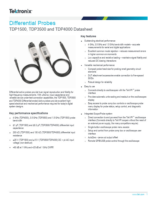
Differential ProbesTDP1500, TDP3500 and TDP4000 DatasheetDifferential active probes provide truer signal reproduction and fidelity for high-frequency measurements. With ultra-low input capacitance andversatile device-under-test connection capabilities, the TDP1500, TDP3500and TDP4000 Differential-ended Active probes provide excellent high-speed electrical and mechanical performance required for today's digital system designs.Key performance specifications4 GHz (TDP4000), 3.5 GHz (TDP3500) and 1.5 GHz (TDP1500) probebandwidth≤1 pF (TDP1500) and ≤0.3 pF (TDP3500/TDP4000) differential inputcapacitance200 kΩ (TDP1500) and 100 kΩ (TDP3500/TDP4000) differential inputresistance±25 V (TDP1500) and ±15 V (TDP3500/TDP4000) DC + pk AC inputvoltage (non-destruct)>60 dB at 1 MHz and >25 dB at 1 GHz CMRRKey featuresOutstanding electrical performance4 GHz, 3.5 GHz and 1.5 GHz bandwidth models - accuratemeasurements for serial and digital applicationsExcellent common mode rejection – reduces measurement errorsin higher common environmentsLow capacitive and resistive loading – maintains signal fidelity andreduces DC biasing interactionsVersatile mechanical performanceCompact probe head size for probing small geometry circuitelementsDUT attachment accessories enable connection to fine-spacedSMDsRobust design for reliabilityEasy to useConnects directly to oscilloscopes with the TekVPI ™ probeinterfaceProvides automatic units scaling and readout on the oscilloscopesdisplayEasy access to probe comp box controls or oscilloscope probe menu display for probe status, setup control, and diagnosticinformationIntegrated Scope/Probe systemDirect connection to and powered from the TekVPI ™ oscilloscope interface (Connects directly to TekVPI scopes without the need ofan external power supply, like many competitors require)Single-button oscilloscope probe menu accessSetup and control from probe comp box or oscilloscope userinterfaceAutoZero - zeros out output offsetRemote GPIB/USB probe control through the oscilloscopeApplicationsDesign, validation, debugging, and characterization of common high-speed serial bus designs:I 2CCAN/LINSPISerial ATAEthernet (GbE)USB 2.0FIreWire (1394b)Signal integrity, jitter, and timing analysisManufacturing, engineering, and testA better measurement toolSpecifically designed for use and direct connection to oscilloscopes with the TekVPI ™ probe interface, the TDP1500, TDP3500 and TDP4000Differential probes achieve high-speed signal acquisition and measurementfidelity by solving three traditional problems:DUT loading effects - Are reduced by lower input capacitance and highinput resistanceDUT connectivity - A variety of accessories exist for attaching to smallSMDs, some come standard or recommendedMaximizing of system (oscilloscope and probe) bandwidth - Probing solutions for all measurements for TekVPI interface oscilloscope models up to 4 GHzFor the best probe support, download and install the latest version of the oscilloscope software from /software/downloads .DatasheetTDP1500, TDP3500 and TDP4000 Differential probesSpecificationsAll specifications are guaranteed unless noted otherwise. All specifications apply to all models unless noted otherwise.Warranted characteristicsBandwidth (probe only)TDP1500≥1.5 GHz warrantedRise time (probe only)TDP3500≤140 psAttenuationTDP15001X, 10XTDP35005XCMRR>60 dB at 1 MHz, >25 dB at 1 GHzMaximum input voltage(nondestruct)TDP1500±25 V (DC + pk AC)TDP3500±15 V (DC + pk AC)TDP4000±15 V (DC + pk AC)Typical characteristicsBandwidth (probe only)TDP3500≥3.5 GHzTDP4000≥4 GHzRise time (probe only)TDP1500≤265 psTDP4000≤125 psDifferential input capacitanceTDP1500≤1 pFTDP3500≤0.3 pFTDP4000≤0.3 pFDifferential input resistanceTDP1500200 kΩTDP3500100 kΩTDP4000100 kΩNoise levelTDP1500<≈≈Propagation delay 5.4 nsCommon mode input rangeTDP1500±7 V (1X)±7 V (10X)TDP3500+5 V to -4 V TDP4000+5 V to -4 V Input offset rangeTDP1500±7 V (10X or 1X)TDP3500±1 V displayed TDP4000±1 V displayed Differential input dynamic rangeTDP1500±8.5 V (10X)±850 mV (1X)TDP3500±2 V TDP4000±2 VNominal characteristicsRecommended oscilloscope interfaceTekVPI ™ ProbePower requirementsPower requirementsPowered directly by oscilloscopes with the TekVPI probe interface.Physical characteristicsDimensionsWeight1Typical for TDP1500.2Typical for TDP1500.DatasheetTypical characteristicsTDP1500, TDP3500 and TDP4000 Differential probes Ordering informationModelsTDP1500 1.5 GHz Differential Probe with TekVPI™ Probe Interface, Certificate of Traceable Calibration Standard.TDP3500 3.5 GHz Differential Probe with TekVPI™ Probe Interface, Certificate of Traceable Calibration Standard.TDP4000 4 GHz Differential Probe with TekVPI™ Probe Interface, Certificate of Traceable Calibration Standard.OptionsLanguage optionsOpt. L0English manualOpt. L5Japanese manualOpt. L7Simplified Chinese manualService optionsOpt. C3Calibration Service 3 YearsOpt. C5Calibration Service 5 YearsOpt. D1Calibration Data ReportOpt. D3Calibration Data Report 3 Years (with Opt. C3)Opt. D5Calibration Data Report 5 Years (with Opt. C5)Opt. R3Repair Service 3 Years (including warranty)Opt. R5Repair Service 5 Years (including warranty)Opt. SILV900Standard warranty extended to 5 yearsAccessoriesTDP1500 standard accessoriesDatasheetTDP3500 and TDP4000 standard accessoriesRecommended accessoriesTektronix is registered to ISO 9001 and ISO 14001 by SRI Quality System Registrar.Product(s) complies with IEEE Standard 488.1-1987, RS-232-C, and with Tektronix Standard Codes and Formats.TDP1500, TDP3500 and TDP4000 Differential probesDatasheetASEAN / Australasia (65) 6356 3900 Austria 00800 2255 4835*Balkans, Israel, South Africa and other ISE Countries +41 52 675 3777 Belgium 00800 2255 4835*Brazil +55 (11) 3759 7627 Canada180****9200Central East Europe and the Baltics +41 52 675 3777 Central Europe & Greece +41 52 675 3777 Denmark +45 80 88 1401Finland +41 52 675 3777 France 00800 2255 4835*Germany 00800 2255 4835*Hong Kong 400 820 5835 India 000 800 650 1835 Italy 00800 2255 4835*Japan 81 (3) 6714 3086 Luxembourg +41 52 675 3777 Mexico, Central/South America & Caribbean 52 (55) 56 04 50 90Middle East, Asia, and North Africa +41 52 675 3777 The Netherlands 00800 2255 4835*Norway 800 16098People's Republic of China 400 820 5835 Poland +41 52 675 3777 Portugal 80 08 12370Republic of Korea +822 6917 5084, 822 6917 5080 Russia & CIS +7 (495) 6647564 South Africa +41 52 675 3777Spain 00800 2255 4835*Sweden 00800 2255 4835*Switzerland 00800 2255 4835*Taiwan 886 (2) 2656 6688 United Kingdom & Ireland 00800 2255 4835*USA180****9200* European toll-free number. If not accessible, call: +41 52 675 3777For Further Information. Tektronix maintains a comprehensive, constantly expanding collection of application notes, technical briefs and other resources to help engineers working on the cutting edge of technology. Please visit . Copyright © Tektronix, Inc. All rights reserved. Tektronix products are covered by U.S. and foreign patents, issued and pending. Information in this publication supersedes that in all previously published material. Specification andprice change privileges reserved. TEKTRONIX and TEK are registered trademarks of Tektronix, Inc. All other trade names referenced are the service marks, trademarks, or registered trademarks of their respective companies.16 Jul 2018 51W-20565-8 。
LED驱动控制专用电路TM1628说明书

一、概述TM1628是一种带键盘扫描接口的LED(发光二极管显示器)驱动控制专用IC,内部集成有MCU 数字接口、数据锁存器、LED 驱动、键盘扫描等电路。
本产品质量可靠、稳定性好、抗干扰能力强。
主要适用于家电设备(智能热水器、微波炉、洗衣机、空调、电磁炉)、机顶盒、电子称、智能电表等数码管或LED显示设备。
二、特性说明•采用CMOS工艺•多种显示模式(10 段×7 位~ 13段×4 位)••••••••三、四、管脚功能定义:五、指令说明:指令用来设置显示模式和LED驱动器的状态。
在STB如果在指令或数据传输时STB被置为高电平,串行通讯被初始化,并且正在传送的指令或数据无效(之前传送7位10(3)显示控制命令设置:该指令用来设置显示的开关以及显示亮度调节。
共有8级辉度可供选择进行调节。
略,六、 显示寄存器地址:该寄存器存储通过串行接口接收从外部器件传送到TM1628的数据,最多有效地址从00H-0DH 共14字节单元,分别与芯片SEG 和GRID 管脚对应,具体分配如图(2):写, (图(7)图7给出共阴极数码管的连接示意图,如果让该数码管显示“0”,只需要向00H (GRID1)地址中从低位开2、驱动共阳极数码管:、该芯片最大支持的键扫矩阵为10×2bit,如下所示:图(3)键扫数据储存地址如下所示,先发读按键命令后,开始读取5字节的按键数据BYTE1—BYTE5,读数据从低位开始输出,其中B7和B6位为无效位固定输出为0。
芯片K和KS引脚对应的按键按下时,相对应的字节内的BIT位为1。
▲注意:1、TM1628最多可以读5个字节,不允许多读。
按下时,九、(1需要27位10.....图(10)如图(10)可知,芯片内部按键扫描原理如下:芯片从SEG1/KS1开始逐渐扫描到SEG10/KS10结束,并且SEG1/KS1-SEG8/KS8在一个周期内完成,SEG9/KS9-SEG10/KS10在下一个周期内完成。
集成数字预失真(DPD)算法的宽带RF收发器

集成数字预失真(DPD)算法的宽带RF收发器
ADI公 司扩 充 后 的 RadioVerse产 品 的无线 电设计 ,提高 数据速率 ,改善其 系 列 包 括 新 的 无线 电收 发 器 硬 件 、软 件 在 办 公 楼 、 体 育 馆 、 公 共 交 通 系 统 等 工具 和鲁棒 的设计环境 ,有助于实现 下 人 员密 集 的 高 流 量区 域 中 的连 接 能 力 … 代 网络 昕需 的 尺 ir更 小 、 功 耗 更 低 的 和 数 据 吞 吐 量 。 此 次 发 布 的 产 品 包 括 元线 电。新产品 支持客 户快速评倘 .诈开 AD9375 RFIt ̄;发 器 ,它 是 首 款 片 内 集 发 面 向 4Gt],型 蜂 窝 IllPl’e 5G massive 成 数 字 预 失 真 (DPD)算 法 的 RF收 发 器 。 M IM 0系统 (向 5G过 渡 的 键 构 建 模块 )
雷达 传 感 蠡 德 州 仪 器半 导 体技 术 (上 海 ) 有 限 公 司
台 封 电 源模 块 化 电流 倍 增 器
Vicor Corporation
GD32F3系 列 Cortex —M4 MCU 北 京 兆 易 创 新 科技 股 份 有 限 公 司
EZ USB HX3C C ypress
800V Coof l<10S P7系 歹1 lnfineon
经 过 反 复 的 比 较 和 逮 选 《今 日 电 子 和 21 I c中 国 电 子 网 举 办 的 年 度 产 品 奖 正 式 揭 晓 我 们 借 鉴 了 今 日 电 子 北 美 姊 妹 刊 物 ({Electronic Products ̄杂 志 三 十 余 年 的评 选经 验 ,根 据 以 下 三 方 面 标 ;佳来 评 价 讨 论 并 最 终 确 定 获 奖 名 单 . 产 品 是 否 在 技 术 或 功 能 方 面 有 突 出 的 表 现 : 产 品 是 否 能 够 把 握 技 术 或 应 用 的 发 展 趋 势 并 做 出 相 应 的 改 进 产 品 是 否 易 于 开 发 和 应 用 《今 日 电子 和 21 I c中 国 电 子 网编 辑 部 谩 在 此
TM1637 LED驱动控制专用电路说明书

特性描述TM1637 是一种带键盘扫描接口的LED(发光二极管显示器)驱动控制专用电路,内部集成有MCU 数字接口、数据锁存器、LED 高压驱动、键盘扫描等电路。
本产品性能优良,质量可靠。
主要应用于电磁炉、微波炉及小家电产品的显示屏驱动。
采用DIP20/SOP20的封装形式。
功能特点采用功率CMOS 工艺显示模式(8 段×6 位),支持共阳数码管输出键扫描(8×2bit),增强型抗干扰按键识别电路辉度调节电路(占空比8 级可调)两线串行接口(CLK,DIO)振荡方式:内置RC 振荡内置上电复位电路内置自动消隐电路封装形式:DIP20/SOP20管脚信息GNDSEG1/KS1SEG2/KS2SEG3/KS3SEG4/KS4SEG5/KS5 SEG6/KS6 SEG7/KS7 SEG8/KS8GRID1 GRID2 GRID3 GRID4 GRID5GRID6VDDDIOCLKK1K2 1234567891011121314151617181920管脚功能符号管脚名称管脚号说明DIO 数据输入/输出 17 串行数据输入/输出,输入数据在SLCK 的低电平变化,在SCLK 的高电平被传输,每传输一个字节芯片内部都将在第八个时钟下降沿产生一个ACK CLK 时钟输入 18 在上升沿输入/输出数据K1~K2 键扫数据输入 19-20 输入该脚的数据在显示周期结束后被锁存 SG1~SG8 输出(段) 2-9 段输出(也用作键扫描),N 管开漏输出 GRID6~GRID1输出(位) 10-15 位输出,P 管开漏输出 VDD 逻辑电源 16 接电源正 GND逻辑地1接系统地在干燥季节或者干燥使用环境内,容易产生大量静电,静电放电可能会损坏集成电路,天微电子建议采取一切适当的集成电路预防处理措施,如果不正当的操作和焊接,可能会造成ESD 损坏或者性能下降, 芯片无法正常工作。
读键扫数据键扫矩阵为8×2bit ,如下所示:S1S5S9S13S2S6S10S14S3S7S11S15S4S8S12S16K1K2S G 1S G 2S G 3S G 4S G 5S G 6S G 7S G 8在有按键按下时,读键数据如下:(低位在前,高位在后)SG1SG2SG3SG4SG5SG6SG7SG8K1 1110_1111 0110_1111 1010_1111 0010_1111 1100_1111 0100_1111 1000_1111 0000_1111 K2 1111_01110111_01111011_01110011_01111101_01110101_01111001_01110001_0111注意:在无按键按下时,读键数据为:1111_1111,低位在前,高位在后。
TD2072B光纤收发芯片

JIAXINGHEROIC T ECHNOLOGY Co., Ltd
Page 2 of 14
10/2012, V1.3
Pin Description (for QFN24L package)
TD2072B
P in Number
1 2
3 4 5 6 7 8 9
10 11 12 13 14 15
TD2072B
TD2072B
+3.3V, 155Mbps to 300Mbps Limiting Amplifier with Integrated Laser Diode Driver
General Description
T he T D2072B is a single chip integrated limiting amplifier (LA) and laser diode driver (LD) for application in optical communication systems with operating data rates from 155Mbps to 300Mbps.
- 1、下载文档前请自行甄别文档内容的完整性,平台不提供额外的编辑、内容补充、找答案等附加服务。
- 2、"仅部分预览"的文档,不可在线预览部分如存在完整性等问题,可反馈申请退款(可完整预览的文档不适用该条件!)。
- 3、如文档侵犯您的权益,请联系客服反馈,我们会尽快为您处理(人工客服工作时间:9:00-18:30)。
・单片全集成限幅放大器(LA )和激光二极管驱动器(LD )的收发器3.3V 单电源供电
工作速率155Mbps ~1.25Gbps 集成自动功率控制(APC )电路调制电流 (IMOD) 可达80mA 偏置电流 (IBIAS) 可达80mA
1.2mV LA 输入幅度(BER=10 )可编程 LOS 电平和 LOS 释放时间无噪音信号丢失(LOS )输出–≤
2.0dB 电学回滞
–内部 5kΩ 上拉电阻的 OC-TTL 输出–LVPECL 输出
可根据客户需求提供 24-pin QFN(4mmx4mm),28-pin QFN(5mm x 5mm) 或者 LQFP32L 封装
・・・・・・・
・
・EP = Exposed pad is cnnected to GND
+3.3V,155Mbps ~ 1.25Gbps 集成限幅放大器和激光驱动器的收发器
TD2072 是一款集成了限幅放大器(LA )和激光二极管驱动器(LD )的收发器芯片,应用于光纤通信系统,工作速率为155Mbps ~1.25Gbps 。
TD2072 封装形式为小型, 24-pin, 4mmx4mm thin QFN24L ,这在行业中尚属先例,比其它典型的 LA 和 LD 空间可节省50%。
TD2072 为+3.3V±10%单电源供电,环境温度-40°C~+85°C ,排除LD 的偏置和调制电流及LA 输出负载,其典型功耗仅170mW 。
限幅放大器(LA )可检测信号幅度可低至4mV PP ,TD2072 将这些信号进行放大,输出典型800mVPP 的电压限幅波形。
TD2072 包含两个信号丢失(LOS)输出,一
个为内置5kΩ
上拉电阻的开路集电极LVTTL 输出,另一个是LVPECL 输出。
可编程信号丢失电平设置管脚(LOSLVL)
设置跨阻放大器输入幅度的灵敏度。
激光二极管驱动器(LD
)可以实现的调制电流和偏置电流可达80mA 。
管脚布局专门进行优化应用在1X9 光收发模块和SFP/SFF 模块。
-12
・SDH/SONET Ethernet FTTx Receivers
・
・Part Temp range Pin-Package (1)PKG Code TD2072N24-40°C to +85°C 24QFN-EP (2)TD2072N24-1TR (3)TD2072N28(4)-40°C to +85°C 28QFN-EP TD2072N28-1TR TD2072P32(5)-40°C to +85°C
32LQFP
TD2072P32-1TR
(1)All parts are packaged with lead-free.(2)EP =Exposed pad.
(3)TR =1Kpcs Units Tape and Reel
(4)
(5)The package types are available upon request
・A fully integrated single chip limiting amplifier and laser diode driver.A single-supply voltage of +3.3V.
Operating data rates from 155Mbps to 1.25Gbps.
Integrated Automatic Power Control (APC)circuit.
Modulation current (I MOD ) up to 80mA.Bias current (I BIAS ) up to 80mA.
1.2mV Input Amplitude in LA (BER=10 ).Programmable LOS level and LOS release time.
Chatter-free Loss-of-Signal (LOS) outputs – ≤ 2.0dB electrical hysteresis
– OC-TTL output with internal 5kΩ pull-up resistor
– LVPECL output
LVPECL output in LA out put pair with a disable function at a static logic state ‘0’.Available in 24-pin QFN (4mm x 4mm) package. 28-pin QFN (5mm x 5mm) or LQFP32L package is also available upon request.
・・・・・・・・
・
・+3.3V,155Mbps to 1.25Gbps
Limiting Amplifier with Integrated Laser Diode Driver
The TD2072 is a single chip integrated limiting postamplifier (LA) and laser diode driver (LD) for application in optical communication systems with operating data rates from 155Mbps to 1.25Gbps. The TD2072 is packaged in a small, 24-pin,4mm x 4mm thin QFN24L package, which is
unparalleled in the industry. It offers space savings of 50% or more over typical LA and LD.
The TD2072 operates from a single +3.3V±10% power supply, over temperature from -40°C to +85°C and consumes only 170mW (typical), exclusive of bias and modulation currents in LD and out put load in LA. The limiting post amplifier (LA) can detect signals with amplitude as low as 4mV PP . The
TD2072 quantizes these signals and outputs typically 800mV PP voltage-limited waveforms.
It incorporates two loss-of-signal (LOS) outputs, one is the open-collector LVTTL output with internal 5kΩ pull-upresistor and anotheris LVPECL output. A programmable loss-of-signal level set pin
(LOSLVL) sets the sensitivity of the input amplitude detection from the typical transimpedance amplifiers (TIAs).
The laser diode driver (LD) can deliver the modulation current up to 80mA and the bias current up to 80mA.
Its pin assignment is specially optimized for the application in 1X9 optical transceiver module and in SFP / SFF modules.
EP = Exposed pad is cnnected to GND
-12
・SDH/SONET Ethernet FTTx Receivers
・・
Part Temp range Pin-Package (1)PKG Code TD2072N24-40°C to +85°C 24QFN-EP (2)TD2072N24-1TR (3)TD2072N28(4)-40°C to +85°C 28QFN-EP TD2072N28-1TR TD2072P32(5)-40°C to +85°C
32LQFP
TD2072P32-1TR
(1)All parts are
packaged with lead-free.
(2)EP =Exposed pad.
(3)TR =1Kpcs Units Tape and Reel
(4)
(5)The package types are available upon request。