AnalogMixedSignal
电子电路仿真软件EWB
帮助
EWB的工具栏
EWB 5.0 的工具栏
Windows 的通用工具
虚拟仪器仪表的使用方法
电 压 表
选择测量交流电压还是直流电压
设置电压表内阻
虚拟仪器仪表的使用方法
一、指示器件库中的仪表和指示器
此库中的任何一种仪表都可以取出任意多个
文件操作
编辑操作
电路基本操作
电路分析操作
窗口操作
联机帮助操作
占空比设置
单击箭头选择单位
正端
负端
公共端
幅度设置
面板
示波器
图标
A 通道
B 通道
接地端
触发端
A 通道
B 通道
信号输入方式选择
时基控制
触发沿及触 发电平设置
面板扩展
显示方式选择
触发信号选择
面板扩展
拖拽可移动读数指针
指针 1 处的时间和电压读数
指针 2 处的时间和电压读数
指针 1、2处的读数差
电路(Circuit)菜单的功能命令,含义如下: 旋转(Rotate) Ctrl+R 水平倒置(Flip Horizontal) 垂直倒置(Flip Vertical) 元件属性(Component Properties) 放缩(Zoom In、Zoom Out) 电路图选项(Schematic Options)
小 结
编辑(Edit)下拉子菜单,如右图所示,包括: 剪切(Cut) Ctrl+K 复制(Copy) Ctrl+C 粘贴(Paste) Ctrl+V 删除(Delete) Del 全选(Select All) Ctrl+A 复制位图(Copy as Bitmap) Ctrl+I 显示剪贴板(Show clipboard)
数模混合信号电路设计-第一讲

华侨大学IC设计中心
建立层次文件
1.建立config文件 2.链接顶层文件
Mixed Signal Processing & RF/Analog IC TRx architectures Signal IC Digital ASIC
Multi-band Multimode Antenna Interface
AD
90º
AD
Baseband processing
DA
TRx calibration
数模混合信号仿真华侨大学IC设计中心
3.仿真提速
A:用作信 号发生器。 仿真的时候,需要不少的激励信号,而且有着严格的时序关 系,要是用pulse电源或是别的什么电源来做的话,可要累死 人的。用verilog写模块的foundational,就 可以比较方便快 捷的构成一个信号发生器。
B:节约模拟的时间。 对于一些成熟的已经知道电路输入输出特性的电路,可以用 verilog写出其特性,这样的话,模拟的时间可以大大的缩短。 当然,还有就是verilog 的老本家--数字电路,也可以用 verilog写出foundational,节约模拟的时间。
Ch.1概述5
华侨大学IC设计中心
SIP与SOC是两项平行发展的系统集成技术, 它们都顺应了电子产品高性能、多功能、小型 化、轻量化和高可靠性的发展趋势。从发展的 历程来看,SOC与SIP是极为相似的,两者均 希望将逻辑组件、数字、模拟、无源器件整合 在一个单元中。然而就发展方向而言,两者有 很大的不同:SOC是从设计的角度出发,目的 是将一个系统整合到一块IC芯片上去;而SIP 则是由封装的角度出发,将不同功能的芯片整 合于一个电子封装结构体内。
symbo
混合信号仿真_77908259_25107528
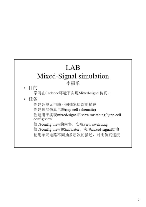
• 目的 • 任务
– 创建各单元电路不同抽象层次的描述 – 创建顶层仿真电路(top cell schematic) – 创建用于实现mixed-signal和view switching的top cell config view – 修改config view的内容,实现view switching – 修改config view和Simulator,实现mixed-signal仿真 – 使用单元电路不同抽象层次的描述,对比仿真速度
10
顶层仿真电路
• 创建用于仿真的电路PLL_SIM schematic
11
查看单元描述
在library manager下可查看各单元各个层次的描述: 行为描述:veriloga view, function view 晶体管级描述: schematic view
请分析各单元的veriloga view的内容, 尽量去理解代码;
19
Mixed-signal仿真
• 特别地, 在config中将Fdiv_20配置为functional view时, 就形成了数模混合仿真, 此时要将simulator由spectre修 改为spectre-Verilog, 并且设置模拟/数字接口特性
Step 1
设置完simulator后, 到simulation->options->digital…下面察看verilog仿真 工具的设置,服务器默认verilog.vmx,不用修改
View switching
后面的仿真设置与 通常的一样 只是现在各单元用 于仿真的view可根 据仿真速度的要求 通过top cell config view来选择切换. 比如Fdiv_20可选择 veriloga或 schematic
assura(for mixed signal)
• Verilog netlist cross-probing • New Short Locator user interface simplifies locating errors • Support for mixed netlist methodologies (DFII schematic, Verilog, CDL) • Extracted view created after LVS run for simulation and probing purposes
• Rule files targeted for .25µm and below: logic, MS/RF, and SiGe • Rule Decks provided by Cadence to the foundries
– Foundry decks available for Assura DRC, LVS, and RCX for major merchant foundries – Supporting Dracula and Diva decks as well for .25 and below
– hypertexted report to locate shorts and opens faster – net and device probing for tracing connections – new rewire function reports required changes to correct the layout
– user selectable sorting mechanisms for error reports – improved error visibility (easy color and stipple pattern customization) – improved error hiding and exception handling (individual or by area)
analoglib中ibis_buffer的使用方法

analoglib中ibis_buffer的使用方法AnalogLib is a library of analog and mixedsignal models, available in Cadence Virtuoso, that enables designers to simulate and verify the performance of their integrated circuits. One of the models provided in AnalogLib is the IBIS buffer model, which is widely used to represent the behavior of input/output buffers in digital designs. In this article, we will discuss the usage of the IBIS buffer model in AnalogLib, step by step.Step 1: Understanding the IBIS Buffer ModelThe IBIS (Input/Output Buffer Information Specification) model is an industrystandard format that describes the electrical behavior of I/O buffers. It provides a standardized way to model the highspeed digital signaling characteristics of a device. The IBIS model encapsulates information such as voltage and current source/sink behaviors, threshold voltage levels, and propagation delays.Step 2: Creating the IBIS Buffer Model in AnalogLibTo create an IBIS buffer model in AnalogLib, follow these steps:1. Launch Cadence Virtuoso and open the Analog Design Environment (ADE).2. Create a new library where you want to store the AnalogLib model.3. Create a new schematic symbol for the IBIS buffer model. This symbol will be used to represent the buffer in the schematic design.4. In the ADE environment, go to the "Create>Symbol" menu and select the library where you want to create the symbol.5. Define the pin names and directions for the IBIS buffer model. These pins represent the I/O ports of the buffer.6. Configure the electrical properties of the pins. This includes specifying the voltage levels, slew rates, and drive strengths of the buffer's I/O ports.7. Save the schematic symbol in the designated AnalogLib library.Step 3: Configuring the IBIS Model ParametersOnce you have created the schematic symbol for the IBIS buffer model, the next step is to configure the IBIS model parameters. The parameters include electrical and timing specifications that define the behavior of the buffer.1. Open the IBIS buffer model in ADE by doubleclicking on the schematic symbol.2. In the "Model Parameters" tab, you can specify the electrical properties of the buffer. This includes parameters like Vih (input high voltage), Vil (input low voltage), Voh (output high voltage), and Vol(output low voltage).3. In the "Timing Specifications" tab, you can define electrical timing characteristics such as setup time, hold time, propagation delay, and transition times.4. Configure any additional parameters required by the specific IBIS model being used. This may include termination resistors, package parasitics, or calibration settings.Step 4: Simulating the IBIS Buffer ModelOnce the IBIS buffer model is configured, you can simulate its behavior to verify its performance. The simulation can be performed on the schematic level using analog simulators like Spectre or Eldo, or on the system level using digital simulators.1. Create a new schematic design where you want to use the IBIS buffer model.2. Place the IBIS buffer symbol from the AnalogLib library onto the schematic, connecting it to the appropriate I/O pins.3. Configure the simulation environment, including the input stimulus and output analysis settings.4. Run the simulation and analyze the results. The simulation will capture the voltage levels, waveform shapes, and timing characteristics of the IBIS buffer under different input conditions.Step 5: Verifying the Performance of the IBIS Buffer ModelAfter simulating the IBIS buffer model, it is crucial to verify its performance against the desired specifications. This can be done by comparing the simulation results with the expected behavior of the buffer.1. Analyze the simulation results to determine if the buffer meets the required voltage levels, timing specifications, and signal integrity requirements.2. If any deviations or discrepancies are observed, analyze the cause of the issues. This may involve reconfiguring the model parameters, modifying the design, or performing additional simulations with different conditions.3. Iterate the design and simulation process until the buffer performance meets the desired specifications.In conclusion, the IBIS buffer model in AnalogLib provides a powerful tool for simulating and verifying the behavior of I/O buffers in digitaldesigns. By following the steps discussed in this article, designers can effectively utilize the IBIS buffer model to ensure the performance and reliability of their integrated circuits.。
ams原理

ams原理AMS是模拟电路设计工具的缩写,全称为Analog/Mixed-Signal。
它是一种基于计算机软件的电路设计工具,能够高效地进行模拟电路设计、仿真以及实现。
本文将简要介绍AMS的设计原理以及其优势。
第一部分:AMS的设计原理AMS的设计原理基于模拟电路的工作原理,即将模拟信号转换为数字信号,使得它们可以在数字系统中进行处理,并且重新将数字信号转换为模拟信号。
主流的AMS软件包括Cadence、Mentor Graphics和Silvaco等。
AMS系统设计流程一般包括以下几个步骤:1. 电路设计:根据设计需求,设计符合规格的电路原理图。
2. 电路仿真:对电路原理图进行仿真,并确定其工作性能和参数。
3. 布局设计:将电路图布局在芯片上,并进行相关规则检查。
4. 版图设计:将电路布局转换成图形,并生成物理版图。
5. 物理验证:对版本进行物理验证,以确保布局所允许的物理约束与实际设计相符合。
第二部分:AMS的优势AMS具有以下几大优势:1. 可重复性:利用AMS的设计工具能够提高设计师的设计效率,减少人工误差,从而提高设计的可重复性。
2. 受限性小:AMS的软件功能强大,可以处理各种不同的电路结构和元器件,因此受限性很小,有更大的灵活性。
3. 可靠性高:AMS软件可以对电路进行全面的仿真,以确保电路的可靠性和安全性。
4. 时间和成本:利用AMS的设计工具,可以节省设计周期,降低成本,减少产量的损失,大大缩短产品上市时间。
综上所述,AMS是一种可重复性强、受限性小、可靠性高、时间和成本都比传统设计方式更加高效的模拟电路设计工具,能够为电路设计师们提供更好的工作体验和更高的产品质量。
Cadence_Mixdsignal_Simulation_tutorial混合仿真

Cadence Mixed-Signal TutorialAssumptionsYou are familiar with the cadence schematic entry toolYou are familiar with running spectre simulations from the analog environmentYou already have a 'cds' directory and know how to create a new projectYou are familiar with VerilogA and Verilog syntaxYou already have a project set up in your cadence environment. This project must use the AMIH processIf you do not have a project setup or you do not have a technology associated with your current project see this tutorial YOU MUST HAVE A TECHNOLOGY ASSOCIATED WITH YOUR CURRENT PROJECT TO DO MIXED-SIGNAL SIMULATIONSBefore you begin1. Open a new terminal, and start icd2. Get the dac_driver.v and ideal_dac.va sourcea. Open a second terminalb. Change directory to "~/cds/project/verilog.src"c. type "wget /~jwade/tutorial/ams_tutorial/dac_driver.v"d. Change directory to "~/cds/project>/veriloga.src"e. type "wget /~jwade/tutorial/ams_tutorial/ideal_dac.va"Where project is your current project.3. Create a new library "amsLib"AGAIN -- YOU MUST HAVE A TECHNOLOGY ASSOCIATED WITH YOUR CURRENT PROJECT TO DO MIXED-SIGNAL SIMULATIONSa. Open the library Managerb. Select file->new->libraryc. Enter amsLib for the name and click "OK"d. Select "Attach to an existing techfile" and click "OK"e. Select "ami500_techlib" and click "OK"Create "ideal_dac" VerilogA module1. open ~/cds/project/veriloga.src/ideal_dac.va in a text editor2. click file->new->cellview in the ICD window3. In the "Create new file" dialog choose...a. Library Name "amsLib"b. Cell Name "ideal_dac"c. View Name "veriloga"d. Tool "VerilogA Editor"e. A module_writer dialog will come up, click cancelf. A new window will open which is running vig. Delete all lines currently in the new window, then paste in the contents of the previously opened ideal_dac.va filei. A dialog box will appear and ask you if you want to create a new symbol, click "Yes"j. A new "Symbol Generate Options dialog will appear. The default values should be ok, but you can change them to suit you.Click "OK" to continue.k. A "Symbol Editing" window will now appear with the new symboll. Click on Design->Check and save in the menu barm. Close the "Symbol Editing" windowCreate dac_driver Verilog module1. Open ~/cds/project/verilog.src/dac_driver.v in a text editor2. Click file->new->cellview in the ICD window3. In the "Create New File" dialog, choose:a. Library Name "amsLib"b. Cell Name "dac_driver"c. View Name "functional"d. Tool "Verilog Editor"4. A new window will open which is running vi5. Delete all lines currently in the new window and then paste in the contents of the previously opened dac_driver.v file6. Hit "esc"->":"->"wq"->"Enter" on the keyboard to save the module7. A new dialog will appear and ask you if you want to create a new symbol, click "Yes"Create test_dac schematic1. Create a new cellview called "test_dac"a. Library Name "amsLib"b. Cell Name "test_dac"c. View Name "Schematic"d. Tool "Composer-Schematic"2. Create the following schematic with the following valuessources, ground, and resistors are from the analogLib librarya. agnd = 2.5Vb. resistor = 100K3. Check and save the schematic4. Close the Schematic Editor windowCreate test_dac config1. Create a new cell view called "test_dac"a. Library Name "amsLib"b. Cell Name "test_dac"c. View Name "config"d. Tool "Hierarchy-Editor"2. A "New Configuration" dialog box will appear3. Click on "Use Template". A new dialog will appear, choose "spectreVerilog" as in the "Name" field. Click "OK"4. You are now back to the "New Configuration" dialog box. You will need to modify the following fields, then click "OK"a. View = "schematic"b. Library List = "amsLib"c. Stop List = "spectre spice"5. In the Hierarchy Editor window, choose View->Update6. In the Hierarchy Editor window, choose File->Save7. Exit the Hierarchy EditorSimulate test_dac1. Open the "test_dac" config view from the ICD window2. A new dialog will appear, choose "yes" for both options3. From the schematic editor window, choose Tools-Analog Environment4. Choose Setup->Simulator/Directory/Host, choose "spectre Verilog" as the simulator, click OK5. Choose Setup->Model Libraries, add $MODS/typ6. Set the transient time to 20.48u, and add any outputs you want to be plotted7. Select Simulation->Netlist and Run. Your outputs should now be plottedConcluding remarksA similar technique can be used to run mixed mode simulations on transistors. Simply add the transistors. This makes it very easy to supply complex input to a circuit to test it by driving it with a verilog test bench. One comment about doing this though. You cannot get analog output directly out of a verilog module. You can only get digital VDD or VSS out. If you want to drive an analog input, use a verilogA DAC to interface the two components.。
了解LDO的psrr_TI

Understanding power supply ripple rejection in linear regulatorsPower supply ripple rejection ratio (PSRR) is a measure of how well a circuit rejects ripple coming from the input power supply at various frequencies and is very critical in many RF and wireless applications. In the case of an LDO,it is a measure of the output ripple compared to the input ripple over a wide frequency range (10 Hz to 10 MHz is common) and is expressed in decibels (dB). The basic equation for PSRR isMore specifically, PSRR for an LDO can be written aswhere A V is the open-loop gain of the regulator feedback loop, and A VO is the gain from V IN to V OUT with the regula-tor feedback loop open. From this equation it can be seenPSRR AA V VO =20log ,PSRR Ripple Ripple InputOutput =20log .that to increase the PSRR it is beneficial to increase the open-loop gain and decrease the gain from V IN to V OUT .Typically, A VO is significantly less than 0 dB, with –10 to –15 dB being typical; this is entirely driven by internal and external parasitics from input to output and at the gate of the pass FET. Figure 1 shows a simplified regulator block diagram with a PMOS pass device.Another parameter that is closely related to PSRR is line transient response. PSRR is specified at specific frequencies,whereas a line transient essentially contains all frequencies due to the Fourier components of a step function. However,the primary difference is that PSRR is based on small signals, whereas line transients are large signals and thus theoretically much more complicated in nature. Sinceimproving PSRR typically improves line transient response and vice versa, all of the effects on PSRR discussed in this article will usually have a similar effect on the line tran-sient response.Texas Instruments IncorporatedPower Management By John C. Teel (Email: jteel@)Analog IC Designer, Member Group Technical StaffTexas Instruments Incorporated Power ManagementA curve showing PSRR over a wide frequency range is shown in Figure 2.As mentioned previously, the open-loop gain of the LDO feedback circuit is the dominant factor in PSRR (at least in a limited frequency range); therefore, LDOs requiring good PSRR typically have high gain with a high unity-gain frequency (large gain-bandwidth product). However, this makes the loop more difficult to stabilize, which limits how much the gain-bandwidth product can be increased to improve PSRR. It is important to have a high unity-gain frequency so that the amplifier does not lose open-loop gain at relatively low frequencies, causing PSRR to roll off also.The curve in Figure 2 shows that PSRR for an LDO can be broken down into three basic frequency regions.Region 1 is from dc to the roll-off frequency of thebandgap filter and is dominated by both open-loop gain and bandgap PSRR. Region 2 extends from the bandgap filter roll-off frequency up to the unity-gain frequency where PSRR is dominated mainly by the open-loop gain of the regulator. Region 3 is above the unity-gain frequency,where the feedback loop has very little effect, so the out-put capacitor dominates along with any parasitics from V IN to V OUT . The gate driver’s ability to drive the pass-FET gate at high frequencies also has an effect in Region 3. A larger output capacitor with less equivalent series resistance (ESR) will typically improve PSRR in this region, but it can also actually decrease the PSRR at some frequencies.This is because increasing the output capacitor lowers the unity-gain frequency, causing the open-loop gain to roll off earlier and thus lowering PSRR. Nevertheless, the minimum PSRR that occurs at the unity-gain frequency will typically be improved.Anything affecting the gain of the feedback loop also affects PSRR in Region 2. One example is load current. As load current increases, the open-loop output impedance of the LDO decreases (since a MOSFET’s output impedance is inversely proportional to the drain current), thus lower-ing the gain. Increasing the load current also pushes the output pole to higher frequencies, which increases the feedback loop bandwidth.The net effect of increasing the load is therefore reduced PSRR at lower frequencies(because of the reduced gain) along with increased PSRR at higher frequencies.The differential dc voltage between input and output is another example of how a change in the feedback loop gain also affects PSRR. As V IN –V OUT is lowered to less than about 1 V, the internal pass FET (which provides gain in a PMOS design) starts to be pushed out of the active (satura-tion)region of operation and into the triode/linear region,which causes the feedback loop to lose gain. The dividing line between the active region and the triode region is proportional to the square root of the drain (load) current.So as the load current is increased, the voltage across the device (V IN –V OUT ) necessary to keep it in the active region increases as a function of the square root of the load cur-rent. For example, having V IN –V OUT at only 0.5 V may have no negative effect on PSRR at light load currents because the pass FET device doesn’t need much headroom to stay in the active region and to preserve gain. At heavier loads,Texas Instruments IncorporatedPower Managementhowever, 0.5 V may no longer be sufficient and the pass FET device may enter the triode region, causing the circuit to lose gain, thus reducing PSRR. When PSRR is compared among various LDOs, it’s important always to compare LDOs with identical V IN –V OUT and I Load conditions. It’s also important to compare LDOs with identical output voltages,since PSRR is usually better at lower output voltages.One of the dominant internal sources of PSRR in an LDO is the bandgap reference. Any ripple that makes its way onto the reference will be amplified and sent to the output, so it’s important to have a bandgap reference with high PSRR. Typically, the solution is simply to filter the bandgap with a low-pass filter (LPF). This LPF is almost always accomplished with a large internal resistor and an external capacitor. The effect of the LPF can be seen in Region 1 of Figure 2, where the PSRR is somewhat reduced because the LPF passes bandgap ripple in this frequency range.As has been shown, there are many ways to improve the PSRR in an LDO application. The most important is to start with a low-noise, high-PSRR LDO designed for high-PSRR applications such as one from the TPS793/4/5/6xx family or the low-I q TPS799xx family. The next most important way is to choose a low-ESR ceramic outputcapacitor and to determine the capacitance value based on the frequencies at which PSRR is most important. Finally,board layout must be carefully done to reduce the feedthrough from input to output via board parasitics.Related Web sites/sc/device/partnumberReplace partnumber with TPS79301, TPS79401,TPS79501, TPS79601, or TPS79901IMPORTANT NOTICETexas Instruments Incorporated and its subsidiaries (TI) reserve the right to make corrections, modifications, enhancements, improvements, and other changes to its products and services at any time and to discontinue any product or service without notice. Customers should obtain the latest relevant information before placing orders and should verify that such information is current and complete. All products are sold subject to TI's terms and conditions of sale supplied at the time of order acknowledgment. TI warrants performance of its hardware products to the specifications applicable at the time of sale in accordance with TI's standard warranty. Testing and other quality control techniques are used to the extent TI deems necessary to support this warranty. Except where mandated by government requirements, testing of all parameters of each product is not necessarily performed.TI assumes no liability for applications assistance or customer product design. Customers are responsible for their products and applications using TI components. To minimize the risks associated with customer products and applications, customers should provide adequate design and operating safeguards.TI does not warrant or represent that any license, either express or implied, is granted under any TI patent right, copyright, mask work right, or other TI intellectual property right relating to any combination, machine, or process in which TI products or services are used. Information published by TI regarding third-party products or services does not constitute a license from TI to use such products or services or a warranty or endorsement thereof. Use of such information may require a license from a third party under the patents or other intellectual property of the third party, or a license from TI under the patents or other intellectual property of TI. Reproduction of information in TI data books or data sheets is permissible only if reproduction is without alteration and is accompanied by all associated warranties, conditions, limitations, and notices. Reproduction of this information with alteration is an unfair and deceptive business practice. TI is not responsible or liable for such altered documentation.Resale of TI products or services with statements different from or beyond the parameters stated by TI for that product or service voids all express and any implied warranties for the associated TI product or service and is an unfair and deceptive business practice. TI is not responsible or liable for any such statements. Following are URLs where you can obtain information on other Texas Instruments products and application solutions: TI Worldwide Technical Support InternetTI Semiconductor Product Information Center Home PageTI Semiconductor KnowledgeBase Home Page/sc/knowledgebaseProduct Information CentersAmericasPhone+1(972) 644-5580Fax+1(972) 927-6377 Internet/Email /sc/pic/americas.htmEurope, Middle East, and AfricaPhoneBelgium (English)+32 (0) 27 45 54 32Netherlands (English)+31 (0) 546 87 95 45 Finland (English)+358 (0) 9 25173948Russia+7 (0) 95 7850415 France+33 (0) 1 30 70 11 64Spain+34 902 35 40 28 Germany+49 (0) 8161 80 33 11Sweden (English)+46 (0) 8587 555 22 Israel (English)1800 949 0107United Kingdom+44 (0) 1604 66 33 99 Italy800 79 11 37Fax+(49) (0) 8161 80 2045Internet /sc/pic/euro.htmJapanFaxInternational+81-3-3344-5317Domestic0120-81-0036 Internet/EmailInternational /sc/pic/japan.htmDomestic www.tij.co.jp/picAsiaPhoneInternational+886-2-23786800Domestic Toll-Free Number Toll-Free Number Australia1-800-999-084New Zealand0800-446-934China800-820-8682Philippines1-800-765-7404 Hong Kong800-96-5941Singapore800-886-1028Indonesia001-803-8861-1006Taiwan0800-006800Korea080-551-2804Thailand001-800-886-0010 Malaysia1-800-80-3973Fax886-2-2378-6808Email tiasia@ Internet /sc/pic/asia.htm ti-china@C011905 Safe Harbor Statement:This publication may contain forward-looking statements that involve a number of risks and uncertainties. These “forward-looking statements” are intended to qualify for the safe harbor from liability established by the Private Securities Litigation Reform Act of 1995. These forward-looking statements generally can be identified by phrases such as TI or its management “believes,” “expects,” “anticipates,”“foresees,” “forecasts,” “estimates” or other words or phrases of similar import. Similarly, such statements herein that describe the company's products, business strategy, outlook, objectives, plans, intentions or goals also are forward-looking statements. All such forward-looking statements are subject to certain risks and uncertainties that could cause actual results to differ materially from those in forward-looking statements. Please refer to TI's most recent Form 10-K for more information on the risks and uncertainties that could materially affect future results of operations. We disclaim any intention or obligation to update any forward-looking statements as a result of developments occurring after the date of this publication.Trademarks: All trademarks are the property of theirrespective owners.Mailing Address: Texas InstrumentsPost Office Box 655303Dallas, Texas 75265© 2005 Texas Instruments IncorporatedSLYT202。
- 1、下载文档前请自行甄别文档内容的完整性,平台不提供额外的编辑、内容补充、找答案等附加服务。
- 2、"仅部分预览"的文档,不可在线预览部分如存在完整性等问题,可反馈申请退款(可完整预览的文档不适用该条件!)。
- 3、如文档侵犯您的权益,请联系客服反馈,我们会尽快为您处理(人工客服工作时间:9:00-18:30)。
Unlike a simple serial link configuration, such as low-voltage differential signaling (LVDS), a JESD204B interface packs samples of data into defined frames. Each frame boundary of a couple or a few samples is marked by a special control character during the link handshaking, or initial lane alignment sequence (ILAS), from the transmitter. A larger defined group of frames, called a multi-frame, is also marked with a respective control character during the ILAS. However, after this sequence is complete, the control characters are not needed and the full bandwidth of the link can be garnered. Both the frame and multi-frame boundaries are coincident with a frame clock and multi-frame clock respectively.What do JESD204B subclasses mean in relation to deterministic latency?There are three subclasses of the JESD204B protocol to define the deterministic latency of the link. Subclass 0, which is backwards compatible with JESD204 and JESD204A, does not support deterministic latency. Subclass 1 supports deterministic latency by use of a system reference signal called SYSREF. Subclass 2 supports deterministic latency by a dual-purpose use of the ~SYNC signal, which also allows the receiver to initiate the handshaking ILAS routine. The ability to accurately place SYSREF versus ~SYNC in time relative to the clock will dictate which subclass is needed for the system of interest.How can deterministic latency be used to align sampling across multiple converters?For a subclass 1 converter implementation, frame clocks and multi-frame clocks are aligned internally on each device by the occurrence of the system reference edge, SYSREF. When a SYSREF edge is detected, both of these clocks are aligned to that point in time. Since these clocks remain internal to each device, their boundaries within the transmitters are communicated over the serial link by the use of control characters.Each receiver can implicitly decode the placement of the transmitter frame and multi-frame clocks in time relative to its own clocks of the same name and relative to all transmit devices. This enables the receiver to de-skew the samples on the relatively early arrival of data to match the link with the latest arrival of data, using buffer delays (Fig. 2).For synchronous sampling, these data links can be aligned in time within an FPGA. For interleaved sampling, each link can be offset by its corresponding relative phase delay. The deterministic latency can be identified for each link by measuring the delay in time from the receiver’s multi-frame clock edge until each respective link’s multi-frame control character. The caveat here is that the deterministic latency for each link must be shorter than the duration of a multi-frame clock period (Fig. 3).Is deterministic latency the same as total converter latency?The total latency of an ADC is the time it takes an analog sample to be clocked in, processed, and output digitally from the device. Similarly, the total latency of a DAC is the time from when the digital sample data is clocked into the part, until that corresponding sample is clocked out of the analog output. Typically, these are both measured in sample clock periods of resolution, as they are frequency dependent. It is partly a function of the analog processing architecture within the single converter component. This is fundamentally not the same definition as the deterministic latency described by a JESD204B link implementation, which is a function of three components.What is the maximum de-skew budget for aligning multiple converters?The transmitter sends multi-frame control characters to mark the multi-frame clock boundaries during the ILAS process. The receiver identifies these characters to create its own internal local multi-frame clock that is aligned with each of the transmitters in the upstream link. For large array systems where multiple receivers are used, the multi-frame clocks are alsoaligned across all of these devices. Therefore, the deterministic latency of any converter link cannot exceed the time of a single multi-frame clock period. This is the total de-skew time budget across the links.The duration of a multi-frame clock is typically tens of sample clock cycles. It can even be adjusted longer or shorter through setup parameter variables that are communicated during the handshaking of the link.Will this feature correctly align to the same analog sample point on either an ADC or a DAC, or is something more required?Deterministic latency provides a way to align samples based on the same point in time as they are presented to theJESD204B framer. An ADC will have more clock periods of latency in addition to this time that are needed to process an analog sample from its front end ahead of the JESD204B framer. The converter vendor must specify this time period ahead of the framer in duration of clocks. Conversely, a DAC will need additional clock periods after the de-framer to process a sample to the output in analog form.How long does the alignment process take before valid analog sample data is available?A SYSREF edge sent to the converter and FPGA causes an alignment process to start. After this event, several multi-frame clock periods, in addition to the ILAS sequence, are required to complete before valid sample data is available. This is equivalent to a relative time of many sample clock periods. The specific duration may depend on unique deterministic delays of the JESD204B core in the converter and the value will need to be communicated by the vendor. During this time, the link will be brought down and valid data will not be transmitted. In absolute time, the duration will be a function of the sample clock frequency.What is the most challenging system design aspect for achieving synchronous sampling?One of the most challenging aspects of achieving synchronous or interleaved processing down to the sample level in subclass 1 is the ability to align the enabling edge of SYSREF in time across multiple converters. In addition, each SYSREF edge will need to meet the setup and hold time to its respective sample clock. This will consume some of the available timing margin. The ability to actively and independently skew the fine phase between SYSREF and the clock will help achieve timing closure across the converters.Does SYSREF need to be a single event or can it be recurring? What do I need to know about each case?SYSREF alignment edges can be a one-shot pulse, periodic, gapped periodic, or recurring non-periodic. This will be dictated by the needs of the system and the timing flexibility of the phase skew between the clock and SYSREF at the source. For a recurring case of SYSREF, the frame and multi-frame clocks will be re-aligned on each event. However, since the goal is to maintain an aligned set of clocks, the enabling edge of a recurring periodic SYSREF should fall on multi-frame clock boundaries. Since the clocks should already be aligned after the first SYSREF edge, this will prevent unnecessary re-alignments.One of the adverse effects of a periodic SYSREF signal is that there is the potential for it to couple onto the analog signal of interest. That’s why a periodic signal isn’t always recommended and should only be used if absolutely necessary. If a periodic SYSREF is used, care must be taken to properly isolate it from the analog front end of an ADC.What are some ways that SYSREF skew can be adjusted to be within a single clock period?Ideally, the SYSREF and clock for each converter and FPGA could be routed precisely, with timing margin to meet thestrict setup and hold times across all components. But with the ever-increasing sample speeds of high-performance converters, timing closure cannot always be met with precise printed-circuit board (PCB) routing alone. Pin-to-pin variance across parts, coupled with supply and temperature drift, can create a relatively large timing skew across an array of high-speed converters. Advanced timing adjustment features may be needed to provide active SYSREF phase skew.For example, an informative alert from an ADC could identify whether the SYSREF edge was latched within the setup and hold keep-out timing window. If this were to occur, ambiguity would exist for which clock edge is used for the timing reference, clock[N] or clock[N+1]. Depending upon where a SYSREF edge was detected, the phase of the sample CLK edge relative to SYSREF could be delayed at the clocking source to maintain a valid timing condition that meets setup and hold time.Another option could be to use the next falling edge of the sample clock instead of the rising edge to get a half period of phase margin. Each converter in the system could be tuned this way, provided the clocking source has independent phase adjustment of the respective SYSREFs and CLKs (Fig. 4).Is a converter with support of subclass 1 or subclass 2 required to use the deterministic latency feature?Subclass 1 and subclass 2 are the only subclasses that support deterministic latency as described in the JESD204B specification. In subclass 1, the SYSREF signal defines the deterministic latency. In subclass 2, the ~SYNC is the signal that defines this latency. Some converter vendors, though, have created a subclass 0 implementation to be used for support of a synchronization scheme that aligns samples. In this case, the alignment procedure of the multi-frame clocks between converters and FPGAs is not used.A time-stamping mechanism at the sample level could be used to mark the occurrence of SYSREF using appended auxiliary information known as control bits. Each sample that is coincident with a SYSREF edge is marked with a uniquecontrol bit. Within the FPGA, each link that has this timestamp can be delayed to equal the longest path and then aligned to each other, independent of the latency differences between the converters (Figures 5 and 6).SummaryWhile deterministic latency is a somewhat complex option of JESD204B, when properly used, it can be a powerful feature for high-performance signal processing system design. Samples from an array of ADCs can be aligned and de-skewed within an FPGA by means of buffer delays to achieve synchronous or interleaved sampling. JESD204B subclassidentification is important to understand the timing alignment capabilities of the system. Timing closure at the SYSREF and CLK input pins across the system ADCs is critical to achieving time aligned samples.Ian Beavers is an applications engineer for the High Speed Converters team at Analog Devices Inc. He has worked for the company since 1999. Ian has over 18 years of experience in the semiconductor industry. He has a bachelor’s degree in electrical engineering from North Carolina State University and an MBA from the University of North Carolina at Greensboro. He is a member of EngineerZone’s High-Speed ADC Support Community. Feel free to send your questionsto IanB on Analog Devices EngineerZone Online Technical Support Community.Source URL:/analog/demystifying-deterministic-latency-within-jesd204b-converters。