7805中文资料
7805资料PDF,7805功能介绍
dB f=120Hz, 8V≤VI≤18V
V
IO=1A, TJ=25℃
mΩ f=1kHz
mA VI=35V, TA=25℃
A
TJ=25℃
2
汕头华汕电子器件有限公司 █ 测试电路
H 7805
图 1、DC 参数测试
图 2、负载调整率测试
图 3、纹波抑制比测试
█ 应用电路
图 4、固定输出稳压器
注: 1)输出电压对应于“XX”值。输入电压,即
静态电流变化率
ΔVO/ΔT 输出电压温度系数
VN
输出噪声电压
RR
纹波抑制比
VD
下降电压
RO
输出阻抗
ISC
短路电流
IPK
峰值电流
4.8 4.75
62
5.0
5.0
4.0 1.6
9 4 5.0 0.03 0.3 -0.8 42 73 2 15 230 2.2
5.2 5.25
TJ=25℃
V
5.OmA≤IO≤1.0A, PD≤15W,
7V≤VI≤20V
100
TJ=25℃, 7V≤VI≤25V
mV
50
TJ=25℃, 8.0mA≤IO≤1.5A
mV
50
TJ=25℃, 250mA≤IO≤750mA
8
mA TJ=25℃
0.5
5mA≤IO≤1.0A
mA
1.3
7V≤VI≤25V
mV/℃ IO=5mA
μV TA=25℃, 10Hz≤f≤100kHz
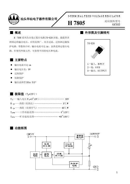
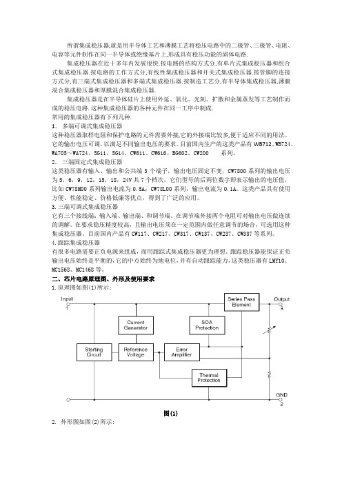
█ 外形图及引脚排列
TO-220
█ 主要特点
输出电流可达 1A 输出电压有:5V 过热保护 短路保护 输出晶体管 SOA 保护
7805中文资料
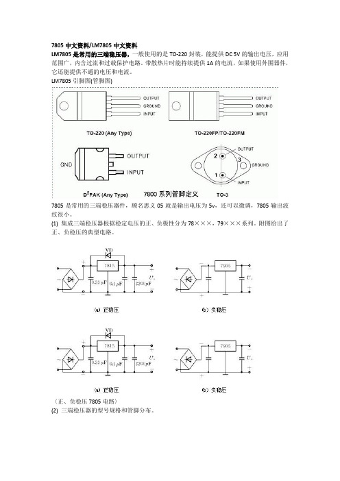
7805中文资料/LM7805中文资料LM7805是常用的三端稳压器,一般使用的是TO-220封装,能提供DC 5V的输出电压,应用范围广,内含过流和过载保护电路。
带散热片时能持续提供1A的电流,如果使用外围器件,它还能提供不通的电压和电流。
LM7805引脚图(管脚图)7805是常用的三端稳压器件,顾名思义05就是输出电压为5v,还可以微调,7805输出波纹很小。
(1) 集成三端稳压器根据稳定电压的正、负极性分为78×××,79×××系列。
附图给出了正、负稳压的典型电路。
〈正、负稳压7805电路〉(2) 三端稳压器的型号规格和管脚分布。
例如:78M05三端稳压器可输出+5 V、A的稳定电压;7912三端稳压器可输出12V、1A的稳定电压。
(3) 外形及管脚分布,如附图1-25所示。
由7805,7905,7812组成的特殊的线性稳压电源如图所示为一种特殊的电源电路。
该电路虽然简单,但可以从两个相同的次级绕组中产生出三组直流电压:+5V、-5V和+12V。
其特点是:D2、D3跨接在E2、E3这两组交流电源之间,起着全波整流的作用。
78057805三端稳压集成电路,电子产品中,常见的三端稳压集成电路有正电压输出的78 ×× 系列和负电压输出的79××系列。
顾名思义,三端IC是指这种稳压用的集成电路,只有三条引脚输出,分别是输入端、接地端和输出端。
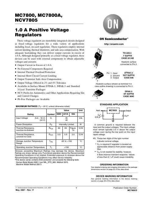
它的样子象是普通的三极管,TO- 220 的标准封装,也有9013样子的TO-92封装。
基本信息中文名称7805三端稳压集成电路最大输出电流特点热过载保护、短路保护、使用方便输入电压不大于36V输入输出压差2V输出电压~结构组成用78/79系列三端稳压IC来组成稳压电源所需的外围元件极少,7805三端稳压集成电路电路内部还有过流、过热及调整管的保护电路,使用起来可靠、方便,而且价格便宜。
NCV7805中文资料
RR
-
VI - VO
-
Vn
-
68
-
2.0
-
10
-
62
83
-
2.0
-
10
-
dB
-
Vnce f = 1.0 kHz
rO
-
0.9
-
-
0.9
-
mW
Short Circuit Current Limit (TA = 25°C) Vin = 35 Vdc
ISC
-
0.2
Q13 QNPN
R6 1.0 k
Q15 QNPN
R20 17500
Q12 QNPN
R12 3.0 k
R25
R16
R10 6.0 k
600
3340-(3316ACT) R26
3.0 k
R9 3.0 k
C1 N+ 30 P
Q4 QNPN
Q2 Q16 QNPN 4
Diode
Q3 QNPN
SUB Q11 2
VO
4.8
5.0
5.2
4.8
5.0
5.2
Vdc
VO
Vdc
-
-
-
4.75
5.0
5.25
4.75
5.0
5.25
-
-
-
Line Regulation (Note 4) 7.5 Vdc ≤ Vin ≤ 20 Vdc, 1.0 A 8.0 Vdc ≤ Vin ≤ 12 Vdc
Load Regulation (Note 4) 5.0 mA ≤ IO ≤ 1.0 A 5.0 mA ≤ IO ≤ 1.5 A (TA = 25°C)
LM7805中文资料

内部结构框图
绝对最大参数值
参数 输入电压(V0=5V~18V)(V0=24V)
热敏电阻接线外壳(Junction cases)(TO-220) 热敏电阻空气接头(Junction-Air) 工作温度范围 存储温度范围
符号 VI VI
RθJC RθJC TOPR TSTG
数值 35 40 5 65 0~+125 -65~+150
4.8 5.0 5.2
V
4.75 5.0 5.25
15W
VI = 7V ~ 20V
电压调整率
Regli TJ=+25 ℃ ne
Vo=7V~25V VI=8V~12V
- 4.0 100 mV - 1.6 50
负载调整率
Regl TJ=+25℃ aod
Io = 5.0mA ~1.5A
-
9 100 mV
Io=250mA
的脉冲测试使用的是负载。
电气特性(MC7806)
(涉及测试电路,0℃< TJ < 125℃, Io= 500mA,VI =11V, CI= 0.33μF,CO= 0.1μF,除非另有说
明)
参数
符号
状态
MC7806
单位
最 Typ 最
小
大
值
值
输出电压
VO TJ=+25℃
5.7 6.0 6.2
V
5.0mA ≤Io≤ 1.0A, PO≤15W,
5
5
5.7 6.0 6.3
VI = 8.0V ~ 21V
电压调整率 Regline TJ=+25℃ VI=8V~25V
- 5 120 mV
VI=9V~13V
MC7805中文资料

3.BOARD OPERATION3.1ACF–II Operating ModeAFC–II has four operating modes. Any one of these modes can be selected using the digital code input to MODE 0 and MODE 1 using ROTARY SW. The function of each mode is as follows.(1)Normal fsc ModeThis is the mode for usual Y/C separation. It separates Y/C from the video signal that is input to the A/D converter.The coring parameter of the vertical enhancer can be set up by the digital code that is input to C0 – C3 (block level parameter), C4 – C7 (white level parameter), and D4 – D7 (noise slice level parameter). The clock is a 3.579545 MHz subcarrier input to the CLK connector; the built–in 4x PLL generates 4xfsc clock.(2)Normal 4xfsc ModeThis mode is used for Y/C separation. It separates Y/C from the video signal that is input to the A/D con-verter.The coring parameter of the vertical enhancer can be set up by the digital code that is input to C0 – C3 (block level parameter), C4 – C7 (white level parameter), and D4 – D7 (noise slice level parameter). The clock is 14.31818 MHz which is a 4x subcarrier input to the CLK connector.(3)Digital Input Comb Filter ModeThis mode uses the A/D converter, filter, and D/A converter as two independent blocks. The digital data converted by the A/D converter is output on C0 – C7. Data input on D0 – D7 is processed by the ACF–II. Filtering is performed by the algorithm of ACF–II and the Y/C video is output as analog signals from Y out and C out. These two blocks can operate with input clock signals that have different frequencies or phases and can be operated independently by using the CLK(AD) for the A/D converter, and the CLK input for the D/A converter.The clock is 14.31818 MHz which is a 4x subcarrier input to the CLK connector and the CLK(AD) con-nector.(4)Digital Output Comb Filter ModeIn addition to the normal Y/C analog outputs, the MC141622EVK can provide the Y/C signals as digital luminance and chrominance signals. The digital luminance data is output on C0 – C7 and the digital chrominance data is output on D0 – D7. This digital data can be modified by other digital processing. MC141622EVK MOTOROLA 24.2Clock Generator CompoundingThe clock generator (MC1378P) provides the necessary reference oscillator and phase locks the clock to the color subcarrier by inputting the composite video signal.VC1 adjusts the horizontal VCO to synchronize the output of the burst gate (pin 5 on the MC1378P) with the input video signal. VC2 adjusts the chroma VCO for maximum amplitude output from the clock buffer (pin 1 on the MC14576).VR3 adjusts pull–in of the chroma PLL filter. This is usually fixed to the center position. VR4 selects the dc bias for the clock buffer output and is usually 2.25 V.4.3Video Amplifier AdjustmentOn the video amplifier (MC14577), the gain is adjusted by VR1. This sets the input range (3.0 Vp–p) of the A/D converter in MC141622FU.VR2 is the clamp level adjustment. This adjusts the sync tip clamping of the input video signal to the video amplifier.4.4Outside InterfaceThe outside interface should provide a composite video input signal to BNC1. The MC141622EVK pro-vides Y/C separation and outputs the luminance from BNC2 and the color signal from BNC3. There is an S output connector on this board for easy connection to instruments having an S input connector.BNC4 and BNC5 are for the external input of each CLK and CLK(AD). However, when using these, it is necessary to modify the board pattern; i.e., cut (J5, J6).There is no filter for bandwidth limitations on this board beyond that imposed by the bandwidth limitations of the MC14577 buffer amplifier. To minimize noise resulting from excessive bandwidth, the bandwidth of input video signal should be limited to no more than one half of the clock frequency.MC141622EVK MOTOROLA 4MC141622EVK MOTOROLA66.MC141622EVK PARTS LISTReference Designation Description IC1MC141622FU IC2MC14576CP IC3MC14577CP IC4MC7805CT IC5MC14576CP IC6MC1378P TR12SC2002TR22SC2002TR32SA953R19.1 k ΩR262 k ΩR3, R475 ΩR5 3.6 k ΩR6750 k ΩR7, R8 2.0 k ΩR9510 ΩR10150 ΩR11510 k ΩR12, R13 2.2 k ΩR1447 k Ω x 4R1547 k Ω x 8R1610 k Ω x 8R1747 k Ω x 8R1810 k Ω x 8R19, R2010 k Ω x 4R21200 ΩR22 1.8 k ΩR23680 ΩR24750 k ΩR25 2.2 k ΩR267.5 m ΩR27 1.0 m ΩR28150 ΩR29470 k ΩL1 – L933 µH L10 4.7 µH L1133 µH VR1 1 k ΩVR2 2.2 k ΩVR3 1 k ΩVR4 1 m ΩVC1, VC230 pF SW1, SW2Toggle Switch DIP SW1, DIP SW28 Channel Dip Switch ROTARY SW16 Channel Switch 4 MHz Cer. Res 14.32 MHz CrystalReference Designation Description C10.1 µF C2, C347 µF C4, C5, C60.1 µF C747 µF C80.1 µF C910 µF C100.1 µF C1110 µF C120.33 µF C131.0 µF C14, C150.1 µF C1647 µF C170.1 µF C18 1.0 µF C1947 µF C20, C210.1 µF C2247 µF C230.1 µF C2447 µF C250.1 µF C2647 µF C2710 µF C280.1 µF C29, C3047 µF C310.1 µF C320.022 µF C33, C34 1.0 µF C350.1 µF C360.001 µF C3747 µF C38 – C450.1 µF C461.0 µF C47, C480.1 µF C49 – C51 1.0 µF C520.1 µF C5347 µF C540.047 µF C55 – C570.1 µF。
7805引脚图管脚电路参数-三端稳压器7805资料
7805引脚图管脚电路参数——三端稳压器7805资料一、7805引脚图及功能说明1. 引脚1(Input):输入端,接入未稳定的直流电压,电压范围通常为7.5V至20V。
3. 引脚3(Output):输出端,输出稳定的5V直流电压。
二、7805管脚电路参数1. 输入电压(Vin):7805的输入电压范围为7.5V至20V,建议输入电压不低于8V,以确保稳压器正常工作。
2. 输出电压(Vout):7805的输出电压为5V,误差范围为±2%。
3. 最大输出电流(Iout):7805的最大输出电流为1.5A,实际输出电流取决于输入电压、负载和散热条件。
4. 线性调整率:7805的线性调整率为0.02%,表示在负载电流不变的情况下,输出电压变化与输入电压变化的比值。
5. 负载调整率:7805的负载调整率为0.1%,表示在输入电压不变的情况下,输出电压变化与负载电流变化的比值。
6.dropout电压:7805的dropout电压为2V,即在输入电压与输出电压之差为2V时,稳压器仍能正常工作。
7. 静态电流(Iq):7805的静态电流为5mA,表示在无负载条件下,稳压器自身消耗的电流。
8. 热关断保护:当7805内部温度超过150℃时,热关断电路将自动切断输出,保护稳压器不受损坏。
9. 短路保护:7805具有短路保护功能,当输出端短路时,稳压器会自动限制输出电流,防止损坏。
三、7805的应用注意事项2. 输入输出电容:为了减少输入输出电压的纹波,通常在7805的输入端和输出端分别接入一个电解电容(如10uF)和一个陶瓷电容(如0.1uF)。
3. 线路布局:在设计电路板时,应尽量缩短输入端和输出端的引线,以减少线路阻抗,提高稳压器的性能。
4. 防止噪声干扰:为了降低噪声对输出电压的影响,可以在7805的接地引脚和电路板的地之间添加一个0欧姆的跳线电阻,以提供一个低阻抗的接地路径。
四、7805的常见问题及解决方案1. 输出电压不稳定:可能是由于输入电压波动大或负载电流变化引起的。
超详细的7805简介与使用说明
7805引脚图管脚电路参数-三端稳压器7805资料
7805引脚图管脚电路参数——三端稳压器7805资料一、7805引脚图及管脚功能1. 引脚1(输入端):连接电源输入,输入电压范围为7.5V至20V。
3. 引脚3(输出端):输出稳定的5V电压,供负载使用。
二、7805电路参数1. 输出电压:5V(误差范围为±1%)2. 最大输出电流:1.5A(在输入电压为12V,输出电压为5V时)3. 线性调整率:±0.02%4. 负载调整率:±0.5%5. 输入电压范围:7.5V至20V6. 静态电流:约6mA(无负载条件下)7. 纹波抑制比:大于60dB8. 工作温度范围:40℃至+125℃三、7805应用电路及注意事项1. 应用电路:7805可应用于各种电子设备,如单片机系统、通信设备、仪表等,为这些设备提供稳定的5V电源。
2. 注意事项:(1)为确保7805正常工作,输入端与输出端之间需接入适当的滤波电容,通常为10μF至100μF。
(2)7805的散热问题不容忽视,尤其在高温环境下或大电流输出时。
建议在7805散热片上涂抹导热硅脂,并确保散热片与散热器之间接触良好。
(3)在接入负载时,请确保负载电流不超过7805的最大输出电流,以免损坏器件。
(4)为防止电路干扰,7805的输入端和输出端应分别接入去耦电容,通常为0.1μF至1μF。
四、7805的安装与调试技巧1. 安装技巧:(1)在安装7805时,请确保引脚顺序正确,避免因引脚错误导致电路无法正常工作或损坏器件。
(2)7805的焊接过程应迅速进行,以免过热损坏器件。
建议使用恒温焊台,并将焊接时间控制在3秒以内。
(3)为防止静电损坏7805,请在焊接前佩戴防静电手环,并在焊接过程中确保工作台面接地。
2. 调试技巧:(1)在电路调试过程中,检查输入电压是否在规定范围内,以确保7805能够正常工作。
(2)使用万用表测量输出电压,观察是否存在波动。
若输出电压不稳定,可适当调整输入端的滤波电容值。
- 1、下载文档前请自行甄别文档内容的完整性,平台不提供额外的编辑、内容补充、找答案等附加服务。
- 2、"仅部分预览"的文档,不可在线预览部分如存在完整性等问题,可反馈申请退款(可完整预览的文档不适用该条件!)。
- 3、如文档侵犯您的权益,请联系客服反馈,我们会尽快为您处理(人工客服工作时间:9:00-18:30)。
三端稳压集成电路 7805
7805概述
电子产品中,常见的三端稳压集成电路有正电压输出的78 ×× 系列和负电压输出的79××系列。
顾名思义,三端IC是指这种稳压用的集成电路,只有三条引脚输出,分别是输入端、接地端和输出端。
它的样子象是普通的三极管,TO- 220 的标准封装,也有9013样子的TO-92封装。
用78/79系列三端稳压IC来组成稳压电源所需的外围元件极少,电路内部还有过流、过热及调整管的保护电路,使用起来可靠、方便,而且价格便宜。
该系列集成稳压IC型号中的78或79后面的数字代表该三端集成稳压电路的输出电压,如7806表示输出电压为正6V,7909表示输出电压为负9V。
因为三端固定集成稳压电路的使用方便,电子制作中经常采用。
注意事项
在实际应用中,应在三端集成稳压电路上安装足够大的散热器(当然小功率的条件下不用)。
当稳压管温度过高时,稳压性能将变差,甚至损坏。
当制作中需要一个能输出1.5A以上电流的稳压电源,通常采用几块三端稳压电路并联起来,使其最大输出电流为N个1.5A,但应用时需注意:并联使用的集成稳压电路应采用同一厂家、同一批
号的产品,以保证参数的一致。
另外在输出电流上留有一定的余量,以避免个别集成稳压电路失效时导致其他电路的连锁烧毁。
编辑本段7805的输入电压范围是多少
78**系列的稳压集成块的极限输入电压是36V,最低输入电压为输出电压的3-4V以上。
7V的电压要想输出5V,则需要使用低压差的稳压集成块,如附图所示的型号。
也可以使用3只普通的整流二极管降压,也能得到5V的较为稳定的电压,二极管的允许电流大于你需要的电流即可。