FPGA可编程逻辑器件芯片XC5VLX155T-1FFG1136C中文规格书
FPGA可编程逻辑器件芯片XC5VSX50T-2FFG1136I中文规格书

模块
最大 RocketIO
收发器(6)
总 I/O
GTP GTX bank(8)
最大 用户 I/O(7)
XC5VLX30
80 x 30 4,800
320
32
64 32 1,522 2 不适用 不适用 不适用 不适用 不适用 13 400
XC5VLX50 120 x 30 7,200
480
和一个写入端口) - 支持 9 位、18 位、36 位和 72 位宽度的存储器位数及奇偶校
验/边带存储器 - 从 32Kx1 到 512x72 的配置(从 8Kx4 到 512x72 用于 FIFO
运行)
• 多速率 FIFO 支持逻辑
- 具有完全可编程近满标志和近空标志的满标志和空标志
DS100 (v5.0) 2009 年 2 月 6 日 产品规范
48
96 48 1,728 6 不适用 不适用 不适用 不适用 不适用 17 560
XC5VLX85
120 x 54 12,960
840
48
192 96 3,456 6 不适用 不适用 不适用 不适用 不适用 17 560
XC5VLX110 XC5VLX155
160 x 54 17,280 160 x 76 24,320
XC5VLX110T 160 x 54 17,280 1,120
64
296 148 5,328 6 不适用
1
XC5VLX 155T 160 x 76 24,320 1,640
128 424 212 7,632 6 不适用
1
4
16 不适用 20 680
4
16 不适用 20 680
FPGA可编程逻辑器件芯片XC5VLX50-1FFG1153I中文规格书

4.08
XC5VLX85
3.52
3.78
4.20
XC5VLX85T
3.52
3.78
4.20
XC5VLX110
3.57
3.84
4.27
XC5VLX110T
3.57
3.84
4.27
XC5VLX155
3.83
4.10
4.53
XC5VLX155T
3.83
4.10
4.53
XC5VLX220
N/A
4.33
4.76
6. TRCKO_FLAGS includes the following parameters: TRCKO_AEMPTY, TRCKO_AFULL, TRCKO_EMPTY, TRCKO_FULL, TRCKO_RDERR, TRCKO_WRERR. 7. TRCKO_POINTERS includes both TRCKO_RDCOUNT and TRCKO_WRCOUNT. 8. The ADDR setup and hold must be met when EN is asserted even though WE is deasserted. Otherwise, block RAM data corruption is possible.
Table 94: Global Clock Setup and Hold With PLL in System-Synchronous Mode
Symbol
Description
Device
Speed Grade
-3
-2
-1
Input Setup and Hold Time Relative to Global Clock Input Signal for LVCMOS25 Standard.(1)
FPGA可编程逻辑器件芯片XC5VSX95T-2FFG1136C中文规格书

© 2006–2010, 2014, 2016 Xilinx, Inc. Xilinx, the Xilinx logo, Artix, ISE, Kintex, Spartan, Virtex, Vivado, Zynq, and other designated brands included herein are trademarks of Xilinx in the United States and other countries. PowerPC is a trademark of IBM Corp. and is used under license. PCI, PCI Express, PCIe, and PCI-X are trademarks of PCI-SIG. All other trademarks are the property of their respective owners.Virtex-5 FPGA Electrical CharacteristicsVirtex®-5 FPGAs are available in -3, -2, -1 speed grades, with -3 having the highest performance. Virtex-5 FPGA DC and AC characteristics are specified for both commercial and industrial grades. Except the operating temperature range or unless otherwise noted, all the DC and ACelectrical parameters are the same for a particular speed grade (that is, the timing characteristics of a -1 speed grade industrial device are the same as for a -1 speed grade commercial device). However, only selected speed grades and/or devices might be available in the industrial range.All supply voltage and junction temperature specifications are representative of worst-case conditions. Theparameters included are common to popular designs and typical applications.This Virtex-5 FPGA data sheet, part of an overall set of documentation on the Virtex-5 family of FPGAs, is available on the Xilinx website:•Virtex-5 Family Overview •Virtex-5 FPGA User Guide•Virtex-5 FPGA Configuration Guide•Virtex-5 FPGA XtremeDSP™ Design Considerations •Virtex-5 FPGA Packaging and Pinout Specification•Embedded Processor Block in Virtex-5 FPGAs Reference Guide•Virtex-5 FPGA RocketIO™ GTP Transceiver User Guide •Virtex-5 FPGA RocketIO GTX Transceiver User Guide •Virtex-5 FPGA Embedded Tri-Mode Ethernet MAC User Guide•Virtex-5 FPGA Integrated Endpoint Block User Guide for PCI Express® Designs•Virtex-5 FPGA System Monitor User Guide •Virtex-5 FPGA PCB Designer’s GuideAll specifications are subject to change without notice.Virtex-5 FPGA DC CharacteristicsProduct SpecificationTable 1:Absolute Maximum RatingsSymbol DescriptionUnits V CCINT Internal supply voltage relative to GND –0.5 to 1.1V V CCAUX Auxiliary supply voltage relative to GND–0.5 to 3.0V V CCO Output drivers supply voltage relative to GND –0.5 to 3.75V V BATT Key memory battery backup supply –0.5 to 4.05V V REFInput reference voltage–0.5 to 3.75V V IN (3)3.3V I/O input voltage relative to GND (4) (user and dedicated I/Os)–0.75 to 4.05V 3.3V I/O input voltage relative to GND (restricted to maximum of 100 user I/Os)(5)–0.95 to 4.4(Commercial Temperature)V –0.85 to 4.3(Industrial Temperature)2.5V or below I/O input voltage relative to GND (user and dedicated I/Os)–0.75 to V CCO +0.5V I IN Current applied to an I/O pin, powered or unpowered±100mA Total current applied to all I/O pins, powered or unpowered±100mA V TS Voltage applied to 3-state 3.3V output (4) (user and dedicated I/Os)–0.75 to 4.05V Voltage applied to 3-state 2.5V or below output (user and dedicated I/Os)–0.75 to V CCO +0.5V T STG Storage temperature (ambient)–65to 150°C T SOL Maximum soldering temperature (2)+220°C T JMaximum junction temperature (2)+125°CNotes:1.Stresses beyond those listed under Absolute Maximum Ratings might cause permanent damage to the device. These are stress ratings only, andfunctional operation of the device at these or any other conditions beyond those listed under Operating Conditions is not implied. Exposure to Absolute Maximum Ratings conditions for extended periods of time might affect device reliability.2.For soldering guidelines, refer to UG112: Device Package User Guide . For thermal considerations, refer to UG195: Virtex-5 FPGA Packaging andPinout Specification on the Xilinx website.3. 3.3V I/O absolute maximum limit applied to DC and AC signals.4.For 3.3V I/O operation, refer to UG190: Virtex-5 FPGA User Guide, Chapter 6, 3.3V I/O Design Guidelines .5.For more flexibility in specific designs, a maximum of 100 user I/Os can be stressed beyond the normal specification for no more than 20% of a data period .找FPGA和CPLD可编程逻辑器件,上深圳宇航军工半导体有限公司DS202 (v5.5) June 17, 2016Table 2:Recommended Operating ConditionsSymbol DescriptionTemperature RangeMin Max Units V CCINT Internal supply voltage relative to GND, T J =0°C to +85°C Commercial 0.95 1.05V Internal supply voltage relative to GND, T J =–40°C to +100°C Industrial 0.95 1.05V V CCAUX (1)Auxiliary supply voltage relative to GND, T J =0°C to +85°C Commercial 2.375 2.625V Auxiliary supply voltage relative to GND, T J =–40°C to +100°C Industrial 2.375 2.625V V CCO (2,4,5)Supply voltage relative to GND, T J =0°C to +85°C Commercial 1.14 3.45V Supply voltage relative to GND, T J =–40°C to +100°C Industrial 1.14 3.45V V IN3.3V supply voltage relative to GND, T J =0°C to +85°C Commercial GND –0.20 3.45V 3.3V supply voltage relative to GND, T J =–40°C to +100°C Industrial GND –0.20 3.45V 2.5V and below supply voltage relative to GND, T J =0°C to +85°CCommercial GND –0.20V CCO +0.2V 2.5V and below supply voltage relative to GND, T J =–40°C to +100°CIndustrial GND –0.20V CCO +0.2V I IN (6)Maximum current through any pin in a powered or unpowered bank when forward biasing the clamp diode Commercial 10mA Industrial 10mA V BATT (3)Battery voltage relative to GND, T J =0°C to +85°C Commercial 1.0 3.6V Battery voltage relative to GND, T J =–40°C to +100°CIndustrial1.03.6VGTX_DUAL Tile SpecificationsGTX_DUAL Tile DC CharacteristicsTable 36:Absolute Maximum Ratings for GTX_DUAL TilesSymbol Description Units MGTAVCCPLL Analog supply voltage for the GTX_DUAL shared PLL relative to GND–0.5 to 1.1V MGTAVTTTX Analog supply voltage for the GTX_DUAL transmitters relative to GND–0.5 to 1.32V MGTAVTTRX Analog supply voltage for the GTX_DUAL receivers relative to GND–0.5 to 1.32V MGTAVCC Analog supply voltage for the GTX_DUAL common circuits relative to GND–0.5 to 1.1V–0.5 to 1.32V MGTAVTTRXC Analog supply voltage for the resistor calibration circuit of the GTX_DUALcolumnSystem Monitor Analog-to-Digital Converter SpecificationTable 51:Analog-to-Digital SpecificationsParameter Symbol Comments/Conditions Min Typ Max UnitsAV DD=2.5V±2%, V REFP=2.5V,V REFN=0V, ADCCLK=5.2MHz, T A=T MIN to T MAX, Typical values at T A=+25°CDC Accuracy: All external input channels such as V P/V N and V AUXP[15:0]/V AUXN[15:0], Unipolar Mode,and Common Mode = 0VResolution10Bits Integral Nonlinearity INL±2LSBsDifferential Nonlinearity DNL No missing codes (T MIN to T MAX)Guaranteed Monotonic±0.9LSBs Unipolar Offset Error(1)Uncalibrated±2±30LSBs Bipolar Offset Error(1)Uncalibrated measured in bipolar mode ±2±30LSBs Gain Error(1)Uncalibrated±0.2±2% Bipolar Gain Error(1)Uncalibrated measured in bipolar mode±0.2±2%Total Unadjusted Error (Uncalibrated)TUE Deviation from ideal transfer function.V REFP–V REFN=2.5V±10LSBsTotal Unadjusted Error (Calibrated)TUE Deviation from ideal transfer function.V REFP–V REFN=2.5V±1±2LSBsCalibrated Gain TemperatureCoefficientVariation of FS code with temperature±0.01LSB/°CDC Common-Mode Reject CMRR DC V N = V CM=0.5V± 0.5V,V P–V N=100mV70dB Conversion Rate(2)Conversion Time - Continuous t CONV Number of CLK cycles2632Conversion Time - Event t CONV Number of CLK cycles21T/H Acquisition Time t ACQ Number of CLK cycles4DRP Clock Frequency DCLK DRP clock frequency8250MHz ADC Clock Frequency ADCCLK Derived from DCLK1 5.2MHz CLK Duty cycle4060% Analog Inputs(3)Dedicated Analog Inputs Input Voltage RangeV P - V N Unipolar Operation01Volts Differential Inputs–0.25+0.25Unipolar Common Mode Range (FS input)0+0.5 Differential Common Mode Range (FS input) +0.3+0.7 Bandwidth20MHzAuxiliary Analog InputsInput Voltage RangeV AUXP[0] /V AUXN[0] to V AUXP[15] /V AUXN[15]Unipolar Operation01Volts Differential Operation–0.25+0.25Unipolar Common Mode Range (FS input)0+0.5 Differential Common Mode Range (FS input)+0.3+0.7 Bandwidth10kHzInput Leakage Current A/D not converting, ADCCLK stopped±1.0µA Input Capacitance10pFOn-chip Supply Monitor Error V CCINT and V CCAUX with calibration enabled±1.0% Reading On-chip Temperature MonitorError–40°C to +125°C with calibration enabled±4°C。
FPGA可编程逻辑器件芯片XQ5VLX155T-2EF1136I中文规格书

General DescriptionThe Defense-grade XQ UltraScale™ architecture-based devices extend the equivalent commercial offerings, adding unique ruggedized packages, extended operating temperature range support, and added environmental qualification testing. This XQ portfolio spans the following families, with each offering a unique mix of features. XQ Kintex® UltraScale FPGAs: High-performance FPGAs with a focus on price/performance, using both monolithic andnext-generation stacked silicon interconnect (SSI) technology. High DSP and block RAM-to-logic ratios and next-generation transceivers, combined with low-cost packaging, enable an optimum blend of capability and cost.XQ Kintex UltraScale+™ FPGAs: Increased performance and on-chip UltraRAM memory to reduce BOM cost. The ideal mix of high-performance peripherals and cost-effective system implementation. Kintex UltraScale+ FPGAs have numerous power options that deliver the optimal balance between the required system performance and the smallest power envelope.XQ Virtex® UltraScale+ FPGAs: The highest transceiver bandwidth, highest DSP count, and highest on-chip and in-package memory available in the UltraScale architecture. Virtex UltraScale+ FPGAs also provide numerous power options that deliver the optimal balance between the required system performance and the smallest power envelope.XQ Zynq® UltraScale+ MPSoCs: Combine the Arm® v8-based Cortex®-A53 high-performance energy-efficient 64-bit application processor with the Arm Cortex-R5 real-time processor and the UltraScale architecture to create the industry's first Defense-grade MPSoCs. Provide unprecedented power savings, heterogeneous processing, and programmable acceleration. XQ Zynq UltraScale+ RFSoCs: Combine RF data converter subsystem and forward error correction with industry-leading programmable logic and heterogeneous processing capability. Integrated RF-ADCs, RF-DACs, and soft-decision FECs (SD-FEC) provide the key subsystems for multiband, multi-mode cellular radios and cable infrastructure.XQ Device ComparisonsDS895 (v2.0) November 15, 2018Product Specification Table 1:Device Resources(1)XQ Kintex UltraScale FPGAXQ KintexUltraScale+FPGAXQ VirtexUltraScale+FPGAXQ ZynqUltraScale+MPSoCXQ ZynqUltraScale+RFSoCMPSoC Processing System✓✓RF-ADC/DAC and SD-FEC✓System Logic Cells (K)530–1,451475–1,143862–2,835154–1,143930 Block Memory (Mb)21.1–75.916.9–34.625.3–70.9 5.1–34.638.0 UltraRAM (Mb)18–3690–2700–3622.5 HBM DRAM (GB)0(2)DSP (Slices)1,920–5,5201,824–1,9682,280–9,216360–3,5284,272 DSP Performance (GMAC/s)(3)7,2973,05014,2845,4686,621 Transceivers16–6416–5640–960–488–16 Max. Transceiver Speed (Gb/s)16.328.228.228.228.2 Max. Serial Bandwidth (full duplex) (Gb/s)2,0862,4025,4161,950902I/O Pins312–728280–512416–83282–644152–408 Notes:1.Metrics given in this table pertain to the XQ ruggedized package devices. For non-ruggedized device variants consult Xilinx sales.2.HBM not currently offered in an XQ ruggedized Package; consult Xilinx sales for further details and options.3.Calculated based on XQ maximum DSP clock rate for a Symmetric FIR Filter, e.g. for KU040 with 1920 DSP48s, -2 speed-grade DSP48F MAX=661MHz, GMACs=2x0.661x1,920=2,538.XQ Kintex UltraScaleXQ Kintex UltraScale+XQ Virtex UltraScale+XQ Zynq UltraScale+ PLXQ Zynq UltraScale+ PSADC10-bit 200kSPS10-bit 200kSPS10-bit 1MSPS Interfaces JTAG, I2C, DRP JTAG, I2C, DRP, PMBus APB•64-bit quad-core Arm Cortex-A53 MPCores. Features associated with each core include: o Arm v8-A Architectureo Operating target frequency: up to 1.5GHzo Single and double precision floating point:4SP/2DP FLOPso NEON Advanced SIMD support with single and double precision floating point instructions o A64 instruction set in 64-bit operating mode, A32/T32 instruction set in 32-bit operating mode o Level 1 cache (separate instruction and data, 32KB each for each Cortex-A53 CPU)–2-way set-associative Instruction Cache with parity support–4-way set-associative Data Cache with ECC supporto Integrated memory management unit (MMU) per processor coreMIO OverviewThe IOP peripherals communicate to external devices through a shared pool of up to 78 dedicated multiplexed I/O (MIO) pins. Each peripheral can be assigned one of several pre-defined groups of pins, enabling a flexible assignment of multiple devices simultaneously. Although 78 pins are not enough for simultaneous use of all the I/O peripherals, most IOP interface signals are available to the PL, allowing use of standard PL I/O pins when powered up and properly configured. Extended multiplexed I/O (EMIO) allows unmapped PS peripherals to access PL I/O.Port mappings can appear in multiple locations. For example, there are up to 12 possible port mappings for CAN pins. The PS Configuration Wizard (PCW) tool aids in peripheral and static memory pin mapping. See Table 17.Transceiver (PS-GTR)The four PS-GTR transceivers, which reside in the full power domain (FPD), support data rates of up to 6.0Gb/s. All the protocols cannot be pinned out at the same time. At any given time, four differential pairs can be pinned out using the transceivers. This is user programmable via the high-speed I/O multiplexer (HS-MIO). •A Quad transceiver PS-GTR (TX/RX pair) able to support following standards simultaneouslyo x1, x2, or x4 lane of PCIe at Gen1 (2.5Gb/s) or Gen2 (5.0Gb/s) rates o 1 or 2 lanes of DisplayPort (TX only) at 1.62Gb/s, 2.7Gb/s, or 5.4Gb/s o 1 or 2 SATA channels at 1.5Gb/s, 3.0Gb/s, or 6.0Gb/s o 1 or 2 USB3.0 channels at 5.0Gb/s o1-4 Ethernet SGMII channels at 1.25Gb/sTable 17:MIO Peripheral Interface MappingPeripheral InterfaceMIOEMIOQuad-SPI NAND YesNo USB2.0: 0,1Yes: External PHY No SDIO 0,1Yes Yes SPI: 0,1I2C: 0,1CAN: 0,1GPIOYesCAN: External PHY GPIO: Up to 78 bits YesCAN: External PHY GPIO: Up to 96 bitsGigE: 0,1,2,3RGMII v2.0: External PHYSupports GMII, RGMII v2.0 (HSTL), RGMII v1.3, MII, SGMII, and 1000BASE-X in Programmable LogicUART: 0,1Simple UART:Only two pins (TX and RX)Full UART (TX, RX, DTR, DCD, DSR, RI, RTS, and CTS) requires either:•Two Processing System (PS) pins (RX and TX) through MIO and sixadditional Programmable Logic (PL) pins, or •Eight Programmable Logic (PL) pinsDebug Trace Ports Yes: Up to 16 trace bits Yes: Up to 32 trace bits Processor JTAGYesYes。
FPGA可编程逻辑器件芯片XQ5VFX70T-2EF1136I中文规格书
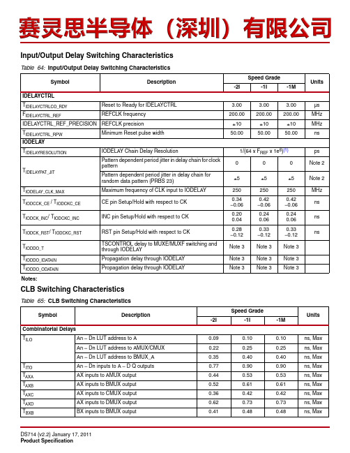
Input/Output Delay Switching CharacteristicsCLB Switching CharacteristicsTable 64:Input/Output Delay Switching CharacteristicsSymbolDescriptionSpeed Grade Units-2I-1I-1MIDELAYCTRL T IDELAYCTRLCO_RDY Reset to Ready for IDELAYCTRL 3.00 3.00 3.00µs F IDELAYCTRL_REF REFCLK frequency 200.00200.00200.00MHz IDELAYCTRL_REF_PRECISION REFCLK precision±10±10±10MHz T IDELAYCTRL_RPW Minimum Reset pulse width50.0050.0050.00nsIODELAYT IDELAYRESOLUTIONIODELAY Chain Delay Resolution1/(64x F REF x 1e 6)(1)ps T IDELAYP AT_JITPattern dependent period jitter in delay chain for clock pattern000Note 2Pattern dependent period jitter in delay chain for random data pattern (PRBS 23)±5±5±5Note 2T IODELAY_CLK_MAX Maximum frequency of CLK input to IODELAY 250250250MHz T IODCCK_CE / T IODCKC_CE CE pin Setup/Hold with respect to CK 0.34–0.060.42–0.060.42–0.06ns T IODCK_INC / T IODCKC_INC INC pin Setup/Hold with respect to CK 0.200.040.240.060.240.06ns T IODCK_RST / T IODCKC_RST RST pin Setup/Hold with respect to CK0.28–0.120.33–0.120.33–0.12nsT IODDO_T TSCONTROL delay to MUXE/MUXF switching and through IODELAYNote 3Note 3Note 3T IODDO_IDA TAIN Propagation delay through IODELAY Note 3Note 3Note 3T IODDO_ODA TAIN Propagation delay through IODELAYNote 3Note 3Note 3Notes:Table 65:CLB Switching CharacteristicsSymbol DescriptionSpeed GradeUnits-2I-1I-1MCombinatorial Delays T ILOAn –Dn LUT address to A0.090.100.10ns, Max An –Dn LUT address to AMUX/CMUX 0.220.250.25ns, Max An –Dn LUT address to BMUX_A0.350.400.40ns, Max T ITO An –Dn inputs to A –D Q outputs 0.770.900.90ns, Max T AXA AX inputs to AMUX output 0.440.530.53ns, Max T AXB AX inputs to BMUX output 0.520.610.61ns, Max T AXC AX inputs to CMUX output 0.360.420.42ns, Max T AXD AX inputs to DMUX output 0.620.730.73ns, Max T BXBBX inputs to BMUX output0.410.480.48ns, MaxCLB Distributed RAM Switching Characteristics (SLICEM Only)CLB Shift Register Switching Characteristics (SLICEM Only)Table 66:CLB Distributed RAM Switching CharacteristicsSymbol DescriptionSpeed GradeUnits-2I-1I-1MSequential Delays T SHCKO Clock to A –B outputs1.26 1.54 1.54ns, Max T SHCKO_1Clock to AMUX –BMUX outputs1.381.681.68ns, MaxSetup and Hold Times Before/After Clock CLK T DS /T DH A –D inputs to CLK 0.840.22 1.030.26 1.030.26ns, Min T AS /T AH Address An inputs to clock 0.460.220.540.270.540.27ns, Min T WS /T WH WE input to clock 0.39–0.040.46–0.020.46–0.02ns, Min T CECK /T CKCECE input to CLK0.42–0.070.51–0.060.51–0.06ns, MinClock CLK T MPW Minimum pulse width 0.82 1.00 1.00ns, Min T MCP Minimum clock period1.642.002.00ns, MinNotes:1. A Zero “0” Hold Time listing indicates no hold time or a negative hold time. Negative values cannot be guaranteed “best-case”, but if a “0” is listed, there is no positive hold time.2.T SHCKO also represents the CLK to XMUX output. Refer to TRACE report for the CLK to XMUX path.Table 67:CLB Shift Register Switching CharacteristicsSymbolDescriptionSpeed GradeUnits-2I-1I-1MSequential Delays T REG Clock to A –D outputs 1.43 1.73 1.73ns, Max T REG_MUX Clock to AMUX –DMUX output 1.55 1.87 1.87ns, Max T REG_M31Clock to DMUX output via M31 output1.151.381.38ns, MaxSetup and Hold Times Before/After Clock CLK T WS /T WH WE input 0.24–0.040.29–0.020.29–0.02ns, Min T CECK /T CKCE CE input to CLK 0.27–0.070.33–0.060.33–0.06ns, Min T DS /T DH A –D inputs to CLK0.660.090.780.110.780.11ns, MinClock CLK T MPW Minimum pulse width 0.700.850.85ns, MinNotes:1.A Zero “0” Hold Time listing indicates no hold time or a negative hold time. Negative values cannot be guaranteed “best-case”, but if a “0” is listed, there is no positive hold time.Block RAM and FIFO Switching Characteristics Table 68:Block RAM and FIFO Switching CharacteristicsSymbol DescriptionSpeed GradeUnits -2I-1I-1MBlock RAM and FIFO Clock to Out DelaysT RCKO_DO and T RCKO_DOR(1)Clock CLK to DOUT output (without output register)(2)(3) 1.92 2.19 2.19ns, MaxClock CLK to DOUT output (with output register)(4)(5)0.690.820.82ns, MaxClock CLK to DOUT output with ECC (without outputregister)(2)(3)3.03 3.61 3.61ns, MaxClock CLK to DOUT output with ECC (with outputregister)(4)(5)0.770.930.93ns, MaxClock CLK to DOUT output with Cascade (without outputregister)(2)2.44 2.94 2.94ns, MaxClock CLK to DOUT output with Cascade (with outputregister)(4)1.07 1.30 1.30ns, Max T RCKO_FLAGS Clock CLK to FIFO flags outputs(6)0.87 1.02 1.02ns, Max T RCKO_POINTERS Clock CLK to FIFO pointer outputs(7) 1.26 1.48 1.48ns, Max T RCKO_ECCR Clock CLK to BITERR (with output register)0.770.930.93ns, Max T RCKO_ECC Clock CLK to BITERR (without output register)2.853.41 3.41ns, MaxClock CLK to ECCP ARITY in standard ECC mode 1.47 1.74 1.74ns, MaxClock CLK to ECCP ARITY in ECC encode only mode0.89 1.05 1.05ns, Max Setup and Hold Times Before/After Clock CLKT RCCK_ADDR/T RCKC_ADDR ADDR inputs(8)0.400.320.480.360.480.36ns, MinT RDCK_DI/T RCKD_DI DIN inputs(9)0.300.280.350.290.350.29ns, MinT RDCK_DI_ECC/T RCKD_DI_ECC DIN inputs with ECC in standard mode(9)0.370.330.420.360.420.47ns, Min DIN inputs with ECC encode only(9)0.720.330.770.360.770.47ns, MinT RCCK_EN/T RCKC_EN Block RAM Enable (EN) input 0.360.150.420.150.420.15ns, MinT RCCK_REGCE/T RCKC_REGCE CE input of output register 0.160.240.180.270.180.27ns, MinT RCCK_SSR/T RCKC_SSR Synchronous Set/ Reset (SSR) input 0.210.250.260.280.260.28ns, MinT RCCK_WE/T RCKC_WE Write Enable (WE) input 0.510.170.630.180.630.18ns, MinT RCCK_WREN/T RCKC_WREN WREN/RDEN FIFO inputs(10)0.410.340.480.400.480.40ns, MinReset DelaysT RCO_FLAGS Reset RST to FIFO Flags/Pointers(11) 1.26 1.48 1.48ns, MaxBPI Master Flash Mode Programming Switching T BPICCO (4)ADDR[25:0], RS[1:0], FCS_B, FOE_B, FWE_B outputs valid after CCLK rising edge101010ns T BPIDCC /T BPICCD Setup/Hold on D[15:0] data input pins3.00.5 3.00.5 3.00.5ns T INITADDRMinimum period of initial ADDR[25:0] address cycles3.03.03.0CCLK cyclesSPI Master Flash Mode Programming Switching T SPIDCC /T SPIDCCD DIN Setup/Hold before/after the rising CCLK edge 4.00.0 4.00.0 5.00.0ns T SPICCM MOSI clock to out 101010ns T SPICCFC FCS_B clock to out101010ns T FSINIT /T FSINITHFS[2:0] to INIT_B rising edge Setup and Hold222µsCCLK Output (Master Modes)T MCCKL Master CCLK clock minimum Low time 3.0 3.0 3.0ns, Min T MCCKHMaster CCLK clock minimum High time3.03.03.0ns, MinCCLK Input (Slave Modes)T SCCKL Slave CCLK clock minimum Low time 2.0 2.0 2.0ns, Min T SCCKH Slave CCLK clock minimum High time2.02.02.0ns, MinDynamic Reconfiguration Port (DRP) for DCM and PLL Before and After DCLKF DCKMaximum frequency for DCLK 450400400MHz T DMCCK_DADDR /T DMCKC_DADDR DADDR Setup/Hold 1.350.0 1.560.0 1.560.0ns T DMCCK_DI /T DMCKC_DI DI Setup/Hold 1.350.0 1.560.0 1.560.0ns T DMCCK_DEN /T DMCKC_DEN DEN Setup/Hold time 1.350.0 1.560.0 1.560.0ns T DMCCK_DWE /T DMCKC_DWE DWE Setup/Hold time 1.350.0 1.560.0 1.560.0ns T DMCKO_DO CLK to out of DO (3) 1.12 1.30 1.30ns T DMCKO_DRDY CLK to out of DRDY1.121.301.30nsNotes:1.Maximum frequency and setup/hold timing parameters are for 3.3V and2.5V configuration voltages.2.T o support longer delays in configuration, use the design solutions described in the Virtex-5 FPGA User Guide .3.DO will hold until next DRP operation.4.Only during configuration, the last edge is determined by a weak pull-up/pull-down resistor in the I/O.Table 70:Configuration Switching Characteristics (Cont’d)SymbolDescriptionSpeed Grade Units-2I-1I-1MSymbolDescriptionDevicesSpeed Grade Units -2I -1I -1M T BCCCK_CE /T BCCKC_CE (1)CE pins Setup/Hold All 0.270.000.310.000.310.00ns T BCCCK_S /T BCCKC_S (1)S pins Setup/HoldAll0.270.000.310.000.310.00ns T BCCKO_O (2)BUFGCTRL delay from I0/I1 to OLX30T, LX85, LX110, LX110T, SX50T , FX70T , FX100T , and FX130T 0.220.250.25nsLX155T0.140.30N/A ns LX220T, LX330T, SX95T , SX240T, and FX200T0.220.25N/AnsMaximum FrequencyF MAXGlobal clock tree (BUFG)LX30T, LX85, LX110, LX110T, SX50T , and FX70T(I)667600N/A MHz LX155T, FX70T(M), and FX100T 600550550MHz FX130T500450N/A MHz LX220T, LX330T, SX95T , SX240T, and FX200T500450N/AMHz。
FPGA可编程逻辑器件芯片XC5VSX95T-1FF1136C中文规格书

Product Specification
General Description
Combining Advanced Silicon Modular Block (ASMBL™) architecture with a wide variety of flexible features, the Virtex®-4 family from Xilinx greatly enhances programmable logic design capabilities, making it a powerful alternative to ASIC technology. Virtex-4 FPGAs comprise three platform families—LX, FX, and SX—offering multiple feature choices and combinations to address all complex applications. The wide array of Virtex-4 FPGA hard-IP core blocks includes the PowerPC® processors (with a new APU interface), tri-mode Ethernet MACs, 622 Mb/s to 6.5 Gb/s serial transceivers, dedicated DSP slices, high-speed clock management circuitry, and source-synchronous interface blocks. The basic Virtex-4 FPGA building blocks are enhancements of those found in the popular Virtex, Virtex-E, Virtex-II, Virtex-II Pro, and Virtex-II Pro X product families, so previous-generation designs are upward compatible. Virtex-4 devices are produced on a state-of-the-art 90 nm copper process using 300 mm (12-inch) wafer technology.
FPGA可编程逻辑器件芯片XC5VSX95T-1FFG1136I中文规格书

XCN11031 (v1.1) June 9, 2015 Product Discontinuation NoticeOverviewThe purpose of this notification is to inform Xilinx customers of the discontinuation of certain Virtex®-4 andVirtex®-5 FPGA devices special part numbers only; devices will continue to ship without change to form, fit, or function, but with updated part numbers.DescriptionSince the introduction of Virtex-4 and Virtex-5 FPGA products, Xilinx has qualified both product families in both Toshiba, in Oita, Japan, and UMC in Taiwan, and has been shipping the majority of devices in each product family from UMC. As part of the consolidation effort described in XCN11030, wafer fabrication for all Virtex-4 and Virtex-5 Devices described in this document will be transferred to UMC.As a result of this transfer, certain part numbers, including SCD and Stepping, will be converted into standard part numbers.For these devices, there is no change to the form, fit, or function of the devices themselves. Qualification data is available in the Xilinx reliability report UG116.Products AffectedThe products affected include all Virtex-4 and Virtex-5 part numbers associated with the following associated SCD and stepping: 0641, 0988, 4009, 4013, 4023, 4058, 4094, 4098, 4108, CS1, CS2 part numbers listed in Table 1, Table 2 and Table 3 below.*Xilinx may cross ship from Toshiba or UMC until Toshiba inventory is depletedXCN11031 (v1.1) June 9, 2015Product Discontinuation Notice For Virtex-4 and Virtex-5 FPGA SCDs from Toshiba Wafer FabricationXCN11031 (v1.1) June 9, 2015Product Discontinuation Notice For Virtex-4 and Virtex-5 FPGA SCDs from Toshiba Wafer FabricationXCN11031 (v1.1) June 9, 2015Product Discontinuation Notice For Virtex-4 and Virtex-5 FPGA SCDs from Toshiba Wafer FabricationXCN11031 (v1.1) June 9, 2015Product Discontinuation Notice For Virtex-4 and Virtex-5 FPGA SCDs from Toshiba Wafer FabricationXCN11031 (v1.1) June 9, 2015。
FPGA可编程逻辑器件芯片XC5VTX150T-3FF1156C中文规格书

Chapter 10:GTX-to-Board InterfaceFully Unused ColumnTable10-13 shows the configuration for Use Case 8, where:• A GTX_DUAL tile is unused•Both transceivers are unused•Boundary-Scan is not functioningTable 10-13:Use Case 8Pin or Pin Pair Connect To FilterMGTRXP/MGTRXN GND-MGTTXP/MGTTXN Floating, no connection-MGTREFCLKP/MGTREFCLKN Floating, no connection-MGTAVTTTX GND-MGTAVTTRX GND-MGTAVTTRXC Floating, no connection-MGTAVCCPLL GND-MGTAVCC GND-MGTRREF GND-Table10-14 shows the configuration for Use Case 9, where:• A GTX_DUAL tile is unused•Both transceivers are unused•Boundary-Scan is functioningTable 10-14:Use Case 9Pin or Pin Pair Connect To FilterMGTRXP/MGTRXN GND-MGTTXP/MGTTXN Floating, no connection-MGTREFCLKP/MGTREFCLKN Floating, no connection-MGTAVTTTX GND-MGTAVTTRX GND-MGTAVTTRXC Floating, no connection-MGTAVCCPLL GND-MGTAVCC V CCINT-MGTRREF GND-RocketIO GTX Transceiver User GuideUG198 (v3.0) October 30, 2009RocketIO GTX Transceiver User Guide UG198 (v3.0) October 30, 2009Chapter 7:GTX Receiver (RX)FPGA RX InterfaceOverviewThe FPGA receives RX data from the GTX receiver through the FPGA RX interface. Data is read from the RXDATA port on the positive edge of RXUSRCLK2.The width of RXDATA can be configured to be one or two bytes wide. The actual width of the port depends on the internal data width of the GTX_DUAL tile, and whether or not the 8B/10B decoder is enabled. Ports widths of 8 bits, 10 bits, 16 bits, 20 bits, 32 bits, and 40 bits are possible.The rate of the parallel clock (RXUSRCLK2) at the interface is determined by the RX line rate, the width of the RXDATA port, and whether or not 8B/10B decoding is enabled. RXUSRCLK must be provided for the internal PCS logic in the receiver. This section shows how to drive the parallel clocks and explains the constraints on those clocks for correct operation.Ports and AttributesTable 7-43 defines the FPGA RX interface ports.Table 7-43:FPGA RX Interface Ports Port Dir Clock Domain DescriptionINT D ATAWI D TH In Async S pecifies the bit width for the TX and RX paths. The bit width of TX and RXmust be identical for both channels.0: 16-bit width1: 20-bit widthREFCLKOUT Out N/A The REFCLKOUT port from each GTX_DUAL tile provides access to thereference clock provided to the shared PMA PLL (CLKIN). It can berouted for use in the FPGA logic.RXDATA0[31:0]RXDATA1[31:0]Out RXUSRCLK2Receive data bus of the receive interface to the FPGA. The width ofRXDATA(0/1) depends on the setting of RXDATAWIDTH(0/1).RXDATAWIDTH0RXDATAWIDTH1In RXUSRCLK2Selects the width of the RXDATA(0/1) receive data connection to theFPGA.0: One-byte interface => RXDATA(0/1)[7:0]1: Two-byte interface => RXDATA(0/1)[15:0]2: Four-byte interface => RXDATA(0/1)[31:0]The clock domain depends on the selected clock (RXRECCLK(0/1),RXUSRCLK(0/1), and RXUSRCLK2(0/1)) for this interface.RXRECCLK0RXRECCLK1Out N/A Recovered clock from the CDR. Clocks the RX logic between the PMAand the RX elastic buffer. Can be used to drive RXUSRCLKsynchronously with incoming data.When RXPOWERDOWN[1:0] is set to 11, which is P2 the lowest powerstate, then RXRECCLK of this transceiver is indeterminate. RXRECCLKof this GTX transceiver is either a static 1 or a static 0.RXRESET0RXRESET1In AsyncPCS RX system reset. Resets the RX elastic buffer, 8B/10B decoder,comma detect, and other RX registers. This is a per channel subset ofGTXRESET.RocketIO GTX Transceiver User Guide UG198 (v3.0) October 30, 2009Chapter 5:Tile FeaturesClockingOverviewFor proper high-speed operation, the GTX transceiver requires a high-quality, low-jitter, reference clock. Because of the shared PMA PLL architecture inside the GTX_DUAL tile, each reference clock sources both channels. The reference clock is used to produce the PLL clock, which is divided by one, two, or four to make individual TX and RX serial clocks and parallel clocks for each GTX transceiver. See “Shared PMA PLL,” page 86 for details.The GTX_DUAL reference clock is provided through the CLKIN port. There are three ways to drive the CLKIN port (see Figure 5-3):•Using an external oscillator to drive GTX dedicated clock routing •Using a clock from a neighboring GTX_DUAL tile through GTX dedicated clock routing •Using a clock from inside the FPGA (GREFCLK)Using the dedicated clock routing provides the best possible clock to the GTX_DUAL tiles. Each GTX_DUAL tile has a pair of dedicated clock pins, represented by IBUFDS primitives, that can be used to drive the dedicated clock routing. Refer to “REFCLK Guidelines” in Chapter 10 for IBUFDS details.This section shows how to select the dedicated clocks for use by one or more GTX_DUAL tiles. Guidelines for driving these pins on the board are discussed in Chapter 10, “GTX-to-Board Interface.”When GREFCLK clocking is used for a specific GTX_DUAL tile, the dedicated clock routing is not used. Instead, the global clock resources of the FPGA are connected to the shared PMA PLL. GREFCLK clocking is not recommended for most designs because of the increased jitter introduced by the FPGA clock nets.The implementation of REFCLKPWRDNB is different between the GTP_DUAL tiles and GTX_DUAL tiles. REFCLKPWRDNB powers down the entire reference clock circuit on the GTP_DUAL tile but only powers down the part of the reference clock circuit that brings in CLKP and CLKN on the GTX_DUAL tile. All other clocks are free to flow, including NORTH, SOUTH, and REFCLK as long as power is applied to the GTX_DUAL tile.。
- 1、下载文档前请自行甄别文档内容的完整性,平台不提供额外的编辑、内容补充、找答案等附加服务。
- 2、"仅部分预览"的文档,不可在线预览部分如存在完整性等问题,可反馈申请退款(可完整预览的文档不适用该条件!)。
- 3、如文档侵犯您的权益,请联系客服反馈,我们会尽快为您处理(人工客服工作时间:9:00-18:30)。
Virtex-5 FPGA Electrical CharacteristicsVirtex®-5 FPGAs are available in -3, -2, -1 speed grades, with -3 having the highest performance. Virtex-5 FPGA DC and AC characteristics are specified for both commercial and industrial grades. Except the operating temperature range or unless otherwise noted, all the DC and ACelectrical parameters are the same for a particular speed grade (that is, the timing characteristics of a -1 speed grade industrial device are the same as for a -1 speed grade commercial device). However, only selected speed grades and/or devices might be available in the industrial range.All supply voltage and junction temperature specifications are representative of worst-case conditions. Theparameters included are common to popular designs and typical applications.This Virtex-5 FPGA data sheet, part of an overall set of documentation on the Virtex-5 family of FPGAs, is available on the Xilinx website:•Virtex-5 Family Overview •Virtex-5 FPGA User Guide•Virtex-5 FPGA Configuration Guide•Virtex-5 FPGA XtremeDSP™ Design Considerations •Virtex-5 FPGA Packaging and Pinout Specification•Embedded Processor Block in Virtex-5 FPGAs Reference Guide•Virtex-5 FPGA RocketIO™ GTP Transceiver User Guide •Virtex-5 FPGA RocketIO GTX Transceiver User Guide •Virtex-5 FPGA Embedded Tri-Mode Ethernet MAC User Guide•Virtex-5 FPGA Integrated Endpoint Block User Guide for PCI Express® Designs•Virtex-5 FPGA System Monitor User Guide •Virtex-5 FPGA PCB Designer’s GuideAll specifications are subject to change without notice.Virtex-5 FPGA DC CharacteristicsDS202 (v5.5) June 17, 2016Product SpecificationTable 1:Absolute Maximum RatingsSymbolDescriptionUnits V CCINT Internal supply voltage relative to GND –0.5 to 1.1V V CCAUX Auxiliary supply voltage relative to GND–0.5 to 3.0V V CCO Output drivers supply voltage relative to GND –0.5 to 3.75V V BATT Key memory battery backup supply –0.5 to 4.05V V REFInput reference voltage–0.5 to 3.75V V IN (3)3.3V I/O input voltage relative to GND (4) (user and dedicated I/Os)–0.75 to 4.05V 3.3V I/O input voltage relative to GND (restricted to maximum of 100 user I/Os)(5)–0.95 to 4.4(Commercial Temperature)V –0.85 to 4.3(Industrial Temperature)2.5V or below I/O input voltage relative to GND (user and dedicated I/Os)–0.75 to V CCO +0.5V I IN Current applied to an I/O pin, powered or unpowered±100mA Total current applied to all I/O pins, powered or unpowered±100mA V TS Voltage applied to 3-state 3.3V output (4) (user and dedicated I/Os)–0.75 to 4.05V Voltage applied to 3-state 2.5V or below output (user and dedicated I/Os)–0.75 to V CCO +0.5V T STG Storage temperature (ambient)–65to 150°C T SOL Maximum soldering temperature (2)+220°C T JMaximum junction temperature (2)+125°CNotes:1.Stresses beyond those listed under Absolute Maximum Ratings might cause permanent damage to the device. These are stress ratings only, andfunctional operation of the device at these or any other conditions beyond those listed under Operating Conditions is not implied. Exposure to Absolute Maximum Ratings conditions for extended periods of time might affect device reliability.2.For soldering guidelines, refer to UG112: Device Package User Guide . For thermal considerations, refer to UG195: Virtex-5 FPGA Packaging andPinout Specification on the Xilinx website.3. 3.3V I/O absolute maximum limit applied to DC and AC signals.4.For 3.3V I/O operation, refer to UG190: Virtex-5 FPGA User Guide, Chapter 6, 3.3V I/O Design Guidelines .5.For more flexibility in specific designs, a maximum of 100 user I/Os can be stressed beyond the normal specification for no more than 20% of a data period .Clock Name Description Reference ClockSpeed GradeUnits -3-2-1Clock-to-out and setup relative to clockT CK_CONTROL CPMMCCLK 1.146 1.247 1.463ps T CK_ADDRESS CPMMCCLK 1.017 1.136 1.38ps T CK_DATA CPMMCCLK 1.076 1.172 1.38ps T CONTROL_CK CPMMCCLK0.7360.8440.941ps T DATA_CK CPMMCCLK0.8340.95 1.058psTable 33:GTP_DUAL Tile User Clock Switching Characteristics(1)Symbol Description ConditionsSpeed GradeUnits -3-2-1F TXOUT TXOUTCLK maximum frequency375375320MHz F RXREC RXRECCLK maximum frequency375375320MHzT RX RXUSRCLK maximum frequency375375320MHz T RX2RXUSRCLK2 maximum frequency RXDATAWIDTH=0350350320MHzRXDATAWIDTH=1187.5187.5160MHz T TX TXUSRCLK maximum frequency375375320MHz T TX2TXUSRCLK2 maximum frequency TXDATAWIDTH=0350350320MHzTXDATAWIDTH=1187.5187.5160MHzNotes:1.Clocking must be implemented as described in UG196: Virtex-5 FPGA RocketIO GTP Transceiver User GuideTable 34:GTP_DUAL Tile Transmitter Switching CharacteristicsSymbol Description Min Typ Max UnitsF GTPTX Serial data rate range0.1F GTPMAX Gb/sT RTX TX Rise time140psT FTX TX Fall time120psT LLSKEW TX lane-to-lane skew(1)855psV TXOOBVDPP Electrical idle amplitude20mVT TXOOBTRANS Electrical idle transition time40nsT J3.75Total Jitter(2) 3.75Gb/s0.35UID J3.75Deterministic Jitter(2)0.19UIT J3.2Total Jitter(2) 3.20Gb/s0.35UID J3.2Deterministic Jitter(2)0.19UIT J2.5Total Jitter(2) 2.50Gb/s0.30UID J2.5Deterministic Jitter(2)0.14UIT J2.0Total Jitter(2) 2.00Gb/s0.30UID J2.0Deterministic Jitter(2)0.14UIT J1.25Total Jitter(2) 1.25Gb/s0.20UID J1.25Deterministic Jitter(2)0.10UIT J1.00Total Jitter(2) 1.00Gb/s0.20UID J1.00Deterministic Jitter(2)0.10UIT J500Total Jitter(2)500Mb/s0.10UID J500Deterministic Jitter(2)0.04UIT J100Total Jitter(2)100Mb/s0.02UID J100Deterministic Jitter(2)0.01UINotes:ing same REFCLK input with TXENPMAPHASEALIGN enabled for up to four consecutive GTP_DUAL sites.ing PLL_DIVSEL_FB=2, INTDATAWIDTH=1.3.All jitter values are based on a Bit-Error Ratio of 1e–12.。