大学物理实验报告 英文版
最新物理实验报告(英文)

最新物理实验报告(英文)Abstract:This report presents the findings of a recent physics experiment conducted to investigate the effects of quantum entanglement on particle behavior at the subatomic level. Utilizing a sophisticated setup involving photon detectors and a vacuum chamber, the experiment aimed to quantify the degree of correlation between entangled particles and to test the limits of nonlocal communication.Introduction:Quantum entanglement is a phenomenon that lies at the heart of quantum physics, where the quantum states of two or more particles become interlinked such that the state of one particle instantaneously influences the state of the other, regardless of the distance separating them. This experiment was designed to further our understanding of this phenomenon and its implications for the fundamental principles of physics.Methods:The experiment was carried out in a controlled environment to minimize external interference. A pair of photons was generated and entangled using a nonlinear crystal. The photons were then separated and sent to two distinct detection stations. The detection process was synchronized, and the data collected included the time, position, and polarization state of each photon.Results:The results indicated a high degree of correlation between the entangled photons. Despite being separated by a significant distance, the photons exhibited a consistent pattern in their polarization states, suggesting a strong entanglement effect. The data also showed that the collapse of the quantum state upon measurement occurred simultaneously for both particles, supporting the theory of nonlocality.Discussion:The findings of this experiment contribute to the ongoing debate about the nature of quantum entanglement and its potential applications. The consistent correlations observed between the entangled particles provide strong evidence for the nonlocal properties of quantum mechanics. This has implications for the development of quantum computing and secure communication technologies.Conclusion:The experiment has successfully demonstrated the robustness of quantum entanglement and its potential for practical applications. Further research is needed to explore the broader implications of these findings and to refine the experimental techniques for probing the quantum realm.References:[1] Einstein, A., Podolsky, B., & Rosen, N. (1935). Can Quantum-Mechanical Description of Physical Reality Be Considered Complete? Physical Review, 47(8), 777-780.[2] Bell, J. S. (1964). On the Einstein Podolsky RosenParadox. Physics, 1(3), 195-200.[3] Aspect, A., Grangier, P., & Roger, G. (1982). Experimental Tests of Realistic Local Theories via Bell's Theorem. Physical Review Letters, 49(2), 91-94.。
Lab-report-物理实验报告(英文)
IntroductionCapacitor is widely used in a variety of fields as it can store electric energy, such as Filtering, resonant circuit and moving phase. Different capacitors have different abilities to store energy, which is due to the difference of capacitance. Capacitance is the ability of a capacitor to store charge in an electric field, it is also a measure of the amount of electric potential energy stored (or separated) for a given electric potential. This report is going to investigate the capacitance of a capacitor made from the experiment by using different DC methods. Before the capacitor made from the experiment is measured, three DC methods will be tested to verify whether these methods are efficient by measuring the capacitance of the known capacitor. In addition, after measuring the unknown capacitor, the whole capacitors will be connected in parallel and the total size of capacitance will be measured.Theory Capacitance can be found by using:dA C r ⨯⨯=εε0. This is for two flat plates. As for the formula, C is the capacitance of a capacitor, A is the area of flat plates, d is the distance between the two flat plates, 0ε is the permittivity of vacuum, r ε is the relative permittivity. Permittivity is constant of proportionality that relates the electric field in a material to the electric displacement in that material and relative permittivity is the ratio of the permittivity of a substance tothat of free space or vacuum. Different materials have different relative permittivity, the behind table includes the relative permittivity of some different material:Source: (The Engineering Tool Box, 2011.) When two capacitors are placed in series, the charge on each plate is of equalof charges on plate and V is the voltage across the capacitor). When ais the initial voltage adding on the capacitor, e is a constant and it is 2.718, R is resistance, C is capacitance and 0I is the initial current flowing through the capacitor). Analogously, when a capacitor is discharged, it flows RC t e V V -=0and RC t eI I -=0.MethodsApparatus :Power supply, leads, ruler, calipers, clips, known capacitor, aluminum foil,。
大学物理实验报告英文版--温度传感器

Physical Lab Report :Temperature SensorsWriter: No:This time in the lab, I come to do something about temperature sensors.Before the experiment, I know that temperature sensors are very widely used lab equipment.From the guide, I can find their outputs changes as a function of temperature.The most commonly used ones in the lab are Platinum resistors and semiconductor thermocouples.In this experiment, I will describe the working principle of Platinum thermo-resistors, Semi-conductor thermo-resistor, and PN diode temperature sensor, and make measurements with them in the lab.At the beginning, I use the ice water to get the reference point to zero degree is 2 degree.So, when I deal with the data, I have changed the temperature into correct ones already.1.Semi-conductor thermo-resistorWithin range, the resistanc-temperature relation is ⎪⎭⎫⎝⎛=T B A R T expIf we calibrate the resistance at a temperature T 0 to be R 0, we can rewrite this relation into⎪⎪⎭⎫⎝⎛-+=0011ln ln T T B R R TAfter I change the unit of temperature into K, I use computer to make a linear fit and get a graph as follows:The slope of the line is equal to 1555.6, it means B=1555.6 K.which is a little bit smaller than the reference.2.Platinum thermo-resistorsA platinum resistor has a temperature-resistance relation of ()201TB AT R R T ++=R/Ω 4000 37023473 3106 2868 2544 2303 2101 1744 1569 1343 1282 1212 1146 1089 118967 896 838 773 724 668 624 586 561 538 505T/C27 30 33 36 39 42 45 48 51 54 57 60 63 66 69 72 75 78 83 88 93 98U/ V 0.1150.11830.12120.12350.1260.12830.13030.13210.13410.13620.1380.13970.14130.1430.14460.14650.14790.14940.15160.15410.15620.1583T/C 14 11 8 5 2 0 -2 -4 -6 -7 -8U/V 0.1064 0.10570.10490.10440.10360.1030.10240.10180.10120.10080.1003From the graph ,I get the coefficient of x2 is B=2.8*10-7 o C-2,the coefficient of x is A=6*10-4 C-13.PN diode temperature sensorT/C 35 38 42 45 47 51 53 55 57 59 61 64 66 98 99 101 103U/V 0.470.4620.450.44140.43660.42460.42010.41380.40750.40170.39580.38840.38350.29610.29290.28840.283T/C 69 72 74 76 78 80 83 85 87 88 90 92 94 96 105 106 110Semiconductor diodes begin conducting electricity only if a certain threshold voltage or cut-in voltage is present in the forward direction.The voltage drop across a forward-biased diode varies only a little with the current, and is a function of temperature; this effect can be used as a temperature sensor.Within a given range of temperature, the resistance varies linearly with temperature.U=-0.0025T+0.5425, as the I=100μA,so,R=-25T+5424,the temperature is 25Error analysis:1.The temperature is tested indirectly, so the measured temperature is a little slower or higher than the correct one,If not precise, then our result of the coefficient is not that correct.2.The ice-water is made by human, even its temperature is near 0, however, there still exists some worry weather it is 0 degree.。
大学物理实验报告英文版--X光
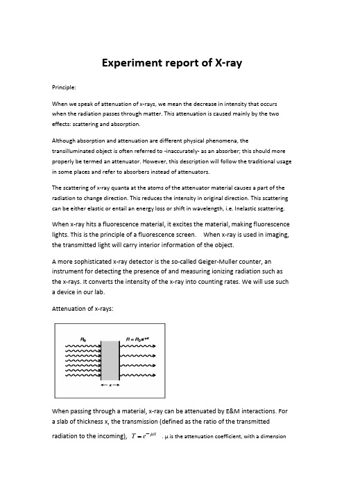
Experiment report of X-rayPrinciple:When we speak of attenuation of x-rays, we mean the decrease in intensity that occurs when the radiation passes through matter. This attenuation is caused mainly by the two effects: scattering and absorption.Although absorption and attenuation are different physical phenomena, the transilluminated object is often referred to -inaccurately- as an absorber; this should more properly be termed an attenuator. However, this description will follow the traditional usage in some places and refer to absorbers instead of attenuators.The scattering of x-ray quanta at the atoms of the attenuator material causes a part of the radiation to change direction. This reduces the intensity in original direction. This scattering can be either elastic or entail an energy loss or shift in wavelength, i.e. Inelastic scattering.When x-ray hits a fluorescence material, it excites the material, making fluorescence lights. This is the principle of a fluorescence screen. When x-ray is used in imaging, the transmitted light will carry interior information of the object.A more sophisticated x-ray detector is the so-called Geiger-Muller counter, an instrument for detecting the presence of and measuring ionizing radiation such as the x-rays. It converts the intensity of the x-ray into counting rates. We will use such a device in our lab.Attenuation of x-rays:When passing through a material, x-ray can be attenuated by E&M interactions. For a slab of thickness x, the transmission (defined as the ratio of the transmittedradiation to the incoming), x=. µ is the attenuation coefficient, with a dimensionT eμ-of 1/distance. µis a character of the material, and it varies, for example, as a function of atomic number. We will study this dependence in this lab. Bragg Diffraction da 0Like normal lights, when x-ray transmit through material with regular optical pattern (e.g. lattice), diffraction will happen if the wavelength of the x-ray is close to the lattice space. Such diffraction on the crystal is the so-called Bragg Diffraction. If the lattice spacing is d, and the x-ray and the crystal surface forms an angle θ, the angle where maximum diffraction happens will satisfy2sin ,1,2,d n n θλ==where n is an integer and λ is the wavelength.Lab equipment:The equipment is an x-ray lab system made by Leybold Inc. A schematic is shown below. 监控区X 光管实验区B1B2B3B4B5A1A2A3A4此区内所有操作必须带上手套进行!!The x-ray is generated by an electron beam with controllable energy (via the potential) and current. The x-ray is going into the detection chamber to the right. There is a removableaperture which focuses the x-ray, a rotatable sample holder, and a rotatable G-M counter. At the right end of the wall, there is a fluorescence screen for imagine.Operation details of the device will be given by the manual. Basically, you need to set the high voltage (U) which determine the energy of the x-ray, the current (I), and the angle of the sample holder (target) or the detector. A knob can be used to make the adjustment on selected parameters. “Coupled” movement means one moves the target and the detector together, the former by an angle α, and the latter by an angle 2α. Make sure the lead glass window is closed before you turn on the high voltage.Attenuator (target)Left: aluminum attenuator mounted on a curved plate with thickness of 0,0.5,1.0,1.5,2.0,2.5, and 3mm. One can select different thickness by selecting angle.Right: attenuation of different materials, all with a thickness of 0.5 mm, including Polystyrene (average Z=6), Aluminum (13), Iron (26), Copper (29), Zirconium(40) andSilver(47).2.Install the aperture. Install the Zr foil onto the aperture. This is to filter out the Kαline. Squeeze the NaCl crystal onto the sample holder.In this part of the procedure we need to make sure that the X ray beam, the crystal surface and the detector is aligned. Use the following alignment procedure by the Bragg Diffraction, the process is omitted.data:The first peak appears when it ’s 7.5 degree.1. analysis:2sin ,1,2,d n n θλ== Then, 9102sin 20.5640210sin 7.5 1.4724101d n θλ--⨯⨯⨯︒===⨯ m. That is, the wavelength of X ray is 101.472410-⨯ m.2.Measure the X ray attenuation to different thickness:Install the Zr foil onto the aperture. Set HV=21 kV, I=0.05 mA, ∆β=0, ∆t=100 s.Hit target key. Change the angle sequentially to 0, 10, 20, 30, 40, 50, 60 degree (the thickness of the attenuation increase by 0.5mm each step).For each of this setting, hit “scan ” to take the data, and hit “replay ” to get the average rate.attenuation of different thicknessthickness(mm) 0.5 1 1.5 2 2.5 3 Data(1/s) 21.4 9.6 4.4 2.8 1.7 1Fit the rate as a function of thickness (with background subtraction) to get the attenuation coefficient.Fit the data in origin with exponential fit (mode = expdec1), through equation x=. We form the graph of 1/T and x.So, we get thatT eμ-Hence,So, the attenuation coefficient is110.263783.79097tμ===.Measure the X ray attenuation to materials with different atomic mass:a)Remove the Zr filter. Insert the curved attenuator holder B (different target) intothe annulus slot on the plastic mount. Set HV = 30 kV, I=1 mA, ∆β=0, ∆t=100 s. Hittarget key. Change the angle sequentially to 0, 10, 20, 30, 40, 50, 60 degree,each corresponding to a given material.b)For each of this setting, hit “scan” to take the data, and hit “replay” to getthe average rate.c)For the scan with Zr filter.attenuation of different Z, with ZrZ 6 13 26 29 40 47 Data(1/s) 9117.9 7627.4 72.9 7.7 108.9 14.4No exact rule can be found.Install the Zr filter. Repeat of Z number.The graph turns out:attenuation of different Z, without ZrZ 6 13 26 29 40 47Data(1/s) 9025.4 9027.8 8308.4 75.2 5.2 74.8Plot the rate as a function of Znumber.Also,no exact rule can be found.Conclusion:1.the wavelength of X ray is 10⨯m.1.472410-2.The rate has no exact relationship with Z.Error:Whether I check the background or not will have a influence on the wavelength. The light in the room will maybe influence the data I got. When I did the experiment with the light on, thus the light will be stronger.。
英语作文物理电学实验报告

英语作文物理电学实验报告Physics Experiment Report on Electric Circuits。
Introduction。
Electric circuits are important in our daily lives as they form the basis of all electrical devices. In this experiment, we investigated the behavior of electric circuits, including Ohm's law, Kirchhoff's laws, and the behavior of resistors in series and parallel.Materials。
Power supply。
Ammeter。
Voltmeter。
Resistors (varying values)。
Wires。
Breadboard。
Procedure。
1. Set up the circuit as shown in the diagram below, using a breadboard to connect the components.2. Measure the voltage across the resistor using the voltmeter and record the value.3. Measure the current flowing through the resistor using the ammeter and record the value.4. Repeat steps 2-3 for different values of resistors.5. Connect resistors in series and parallel and measure the voltage and current across each resistor.Results。
物理实验报告 英文

物理实验报告英文Title: Investigating the Behavior of Light: A Physics Experiment Report Introduction:In this report, we will discuss the experimental setup, procedure, and results of a physics experiment aimed at investigating the behavior of light. Light, as a fundamental entity, exhibits various phenomena that are crucial for understanding the nature of our universe. By conducting this experiment, we aimed to deepen our knowledge of light's properties and its interaction with different materials.Experimental Setup:The experiment was conducted in a controlled laboratory environment with the following equipment:1. Light Source: A laser beam was used as the primary light source. Its monochromatic nature ensured a consistent wavelength throughout the experiment.2. Optical Bench: An optical bench with adjustable components, such as lenses, mirrors, and prisms, was used to manipulate and direct the laser beam.3. Photodetector: A photodetector was employed to measure the intensity of the laser beam after passing through various materials or undergoing different optical processes.Procedure:1. Refraction: The first part of the experiment focused on investigating thephenomenon of refraction. A glass prism was placed on the optical bench, and the laser beam was directed towards it. By varying the angle of incidence, we observed the corresponding change in the angle of refraction. The intensity of the laser beam was measured using the photodetector at different angles.2. Diffraction: In the second part, we explored the phenomenon of diffraction. A diffraction grating was placed in the path of the laser beam. By rotating the grating, we observed the diffraction pattern formed on a screen placed at a specific distance from the grating. The intensity of the diffracted light was measured using the photodetector.3. Interference: The final part of the experiment focused on the interference of light waves. Two narrow slits were placed in the path of the laser beam, creating two coherent sources of light. A screen was placed at a specific distance from the slits, and the interference pattern was observed. The intensity of the interference pattern was measured using the photodetector.Results and Discussion:1. Refraction: As the angle of incidence increased, the angle of refraction also increased. This confirmed the relationship between the two angles predicted by Snell's law. The intensity of the laser beam decreased as the angle of refraction increased, indicating the loss of energy during the refraction process.2. Diffraction: By rotating the diffraction grating, we observed a series of bright and dark fringes on the screen. The distance between the fringes decreased as the grating rotation angle increased, indicating a smaller wavelength ofdiffracted light. The intensity of the laser beam varied at different angles, demonstrating the constructive and destructive interference of light waves.3. Interference: The interference pattern displayed alternating bright and dark fringes. The intensity of the bright fringes was higher, indicating constructive interference, while the dark fringes represented destructive interference. The distance between the fringes increased as the distance from the slits to the screen increased, confirming the relationship between fringe separation and wavelength.Conclusion:Through this experiment, we gained valuable insights into the behavior of light. We observed and analyzed the phenomena of refraction, diffraction, and interference, which are fundamental to the understanding of optics. The results obtained aligned with the theoretical predictions, reinforcing our understanding of light's properties and its interaction with various materials. Conducting experiments such as these allows us to bridge the gap between theoretical knowledge and practical applications, ultimately leading to advancements in the field of physics.。
大学物理实验报告 英文版
大学物理实验报告Ferroelectric Control of Spin PolarizationABSTRACTA current drawback of spintronics is the large power that is usually required for magnetic writing, in contrast with nanoelectronics, which relies on “zero-current,” gate-controlled operations. Efforts have been made to control the spin-relaxation rate, the Curie temperature, or the magnetic anisotropy with a gate voltage, but these effects are usually small and volatile. We used ferroelectric tunnel junctions with ferromagnetic electrodes to demonstrate local, large, and nonvolatile control of carrier spin polarization by electrically switching ferroelectric polarization. Our results represent a giant type of interfacial magnetoelectric coupling and suggest a low-power approach for spin-based information control.Controlling the spin degree of freedom by purely electrical means is currently an important challenge in spintronics (1, 2). Approaches based on spin-transfer torque (3) have proven very successful in controlling the direction of magnetization in a ferromagnetic layer, but they require the injection of high current densities. An ideal solution would rely on the application of an electric field across an insulator, as in existing nanoelectronics. Early experiments have demonstrated the volatile modulation of spin-based properties with a gate voltage applied through a dielectric. Notable examples include the gate control of the spin-orbit interaction in III-V quantum wells (4), the Curie temperature T C (5), or the magnetic anisotropy (6) in magnetic semiconductors with carrier-mediated exchange interactions; for example, (Ga,Mn)As or (In,Mn)As. Electric field–induced modifications of magnetic anisotropy at room temperature have also been reported recently in ultrathin Fe-based layers (7, 8).A nonvolatile extension of this approach involves replacing the gate dielectric by a ferroelectric and taking advantage of the hysteretic response of its order parameter (polarization) with an electric field. When combined with (Ga,Mn)As channels, forinstance, a remanent control of T C over a few kelvin was achieved through polarization-driven charge depletion/accumulation (9, 10), and the magnetic anisotropy was modified by the coupling of piezoelectricity and magnetostriction (11, 12). Indications of an electrical control of magnetization have also been provided in magnetoelectric heterostructures at room temperature (13–17).Recently, several theoretical studies have predicted that large variations of magnetic properties may occur at interfaces between ferroelectrics and high-T C ferromagnets such as Fe (18–20), Co2MnSi (21), or Fe3O4 (22). Changing the direction of the ferroelectric polarization has been predicted to influence not only the interfacial anisotropy and magnetization, but also the spin polarization. Spin polarization [i.e., the normalized difference in the density of states (DOS) of majority and minority spin carriers at the Fermi level (E F)] is typically the key parameter controlling the response of spintronics systems, epitomized by magnetic tunnel junctions in which the tunnel magnetoresistance (TMR) is related to the electrode spin polarization by the Jullière formula (23). These predictions suggest that the nonvolatile character of ferroelectrics at the heart of ferroelectric random access memory technology (24) may be exploited in spintronics devices such as magnetic random access memories or spin field-effect transistors (2). However, the nonvolatile electrical control of spin polarization has not yet been demonstrated.We address this issue experimentally by probing the spin polarization of electrons tunneling from an Fe electrode through ultrathin ferroelectric BaTiO3 (BTO) tunnel barriers (Fig. 1A). The BTO polarization can be electrically switched to point toward oraway from the Fe electrode. We used a half-metallic La0.67Sr0.33MnO3(LSMO) (25) bottom electrode as a spin detector in these artificial multiferroic tunnel junctions (26, 27). Magnetotransport experiments provide evidence for a large and reversible dependence of the TMR on ferroelectric polarization direction.Fig. 1(A) Sketch of the nanojunction defined by electrically controlled nanoindentation. A thin resist is spin-coated on the BTO(1 nm)/LSMO(30 nm) bilayer. The nanoindentation is performed with a conductive-tip atomic force microscope, and the resultingnano-hole is filled by sputter-depositing Au/CoO/Co/Fe. (B) (Top) PFM phase image of a BTO(1 nm)/LSMO(30 nm) bilayer after poling the BTO along 1-by-4–μm stripes with either a negative or positive (tip-LSMO) voltage. (Bottom) CTAFM image of an unpoled area of a BTO(1 nm)/LSMO(30 nm) bilayer. Ω, ohms. (C) X-ray absorption spectra collected at room temperature close to the Fe L3,2 (top), Ba M5,4 (middle), and TiL3,2 (bottom) edges on an AlO x(1.5 nm)/Al(1.5 nm)/Fe(2 nm)/BTO(1 nm)/LSMO(30 nm)//NGO(001) heterostructure. (D) HRTEM and (E) HAADF images of the Fe/BTO interface in a Ta(5 nm)/Fe(18 nm)/BTO(50 nm)/LSMO(30 nm)//NGO(001) heterostructure. The white arrowheads in (D) indicate the lattice fringes of {011} planes in the iron layer. [110] and [001] indicate pseudotetragonal crystallographic axes of the BTO perovskite.The tunnel junctions that we used in this study are based on BTO(1 nm)/LSMO(30 nm) bilayers grown epitaxially onto (001)-oriented NdGaO3 (NGO) single-crystal substrates (28). The large (~180°) and stable piezoresponse force microscopy (PFM) phase contrast (28) between negatively and positively poled areas (Fig. 1B, top) indicates that the ultrathin BTO films are ferroelectric at room temperature (29). The persistence of ferroelectricity for such ultrathin films of BTO arises from the large lattice mismatch with the NGO substrate (–3.2%), which is expected to dramatically enhance ferroelectric properties in this highly strained BTO (30). The local topographical and transport properties of the BTO(1 nm)/LSMO(30 nm) bilayers were characterized by conductive-tip atomic force microscopy (CTAFM) (28). The surface is very smooth with terraces separated by one-unit-cell–high steps, visible in both the topography (29) and resistance mappings (Fig. 1B, bottom). No anomalies in the CTAFM data were observed over lateral distances on the micrometer scale.We defined tunnel junctions from these bilayers by a lithographic technique based on CTAFM (28, 31). Top electrical contacts of diameter ~10 to 30 nm can be patterned by this nanofabrication process. The subsequent sputter deposition of a 5-nm-thick Fe layer, capped by a Au(100 nm)/CoO(3.5 nm)/Co(11.5 nm) stack to increase coercivity, defined a set of nanojunctions (Fig. 1A). The same Au/CoO/Co/Fe stack was deposited on another BTO(1 nm)/LSMO(30 nm) sample for magnetic measurements. Additionally, a Ta(5 nm)/Fe(18 nm)/BTO(50 nm)/LSMO(30 nm) sample and a AlO x(1.5 nm)/Al(1.5nm)/Fe(2 nm)/BTO(1 nm)/LSMO(30 nm) sample were realized for structural and spectroscopic characterizations.We used both a conventional high-resolution transmission electron microscope (HRTEM) and the NION UltraSTEM 100 scanning transmission electron microscope (STEM) to investigate the Fe/BTO interface properties of the Ta/Fe/BTO/LSMO sample. The epitaxial growth of the BTO/LSMO bilayer on the NGO substrate was confirmed by HRTEM and high-resolution STEM images. The low-resolution, high-angle annular dark field (HAADF) image of the entire heterostructure shows the sharpness of theLSMO/BTO interface over the studied area (Fig. 1E, top). Figure 1D reveals a smooth interface between the BTO and the Fe layers. Whereas the BTO film is epitaxially grown on top of LSMO, the Fe layer consists of textured nanocrystallites. From the in-plane (a) and out-of-plane (c) lattice parameters in the tetragonal BTO layer, we infer that c/a = 1.016 ± 0.008, in good agreement with the value of 1.013 found with the use of x-ray diffraction (29). The interplanar distances for selected crystallites in the Fe layer [i.e.,~2.03 Å (Fig. 1D, white arrowheads)] are consistent with the {011} planes ofbody-centered cubic (bcc) Fe.We investigated the BTO/Fe interface region more closely in the HAADF mode of the STEM (Fig. 1E, bottom). On the BTO side, the atomically resolved HAADF image allows the distinction of atomic columns where the perovskite A-site atoms (Ba) appear as brighter spots. Lattice fringes with the characteristic {100} interplanar distances of bcc Fe (~2.86 Å) can be distinguished on the opposite side. Subtle structural, chemical, and/or electronic modifications may be expected to occur at the interfacial boundarybetween the BTO perovskite-type structure and the Fe layer. These effects may lead to interdiffusion of Fe, Ba, and O atoms over less than 1 nm, or the local modification of the Fe DOS close to E F, consistent with ab initio calculations of the BTO/Fe interface (18–20).To characterize the oxidation state of Fe, we performed x-ray absorption spectroscopy (XAS) measurements on a AlO x(1.5 nm)/Al(1.5 nm)/Fe(2 nm)/BTO(1 nm)/LSMO(30 nm) sample (28). The probe depth was at least 7 nm, as indicated by the finite XAS intensity at the La M4,5 edge (28), so that the entire Fe thickness contributed substantially to the signal. As shown in Fig. 1C (top), the spectrum at the Fe L2,3 edge corresponds to that of metallic Fe (32). The XAS spectrum obtained at the Ba M4,5 edge (Fig. 1C, middle) is similar to that reported for Ba2+ in (33). Despite the poor signal-to-noise ratio, the Ti L2,3 edge spectrum (Fig. C, bottom) shows the typical signature expected for a valence close to 4+ (34). From the XAS, HRTEM, and STEM analyses, we conclude that theFe/BTO interface is smooth with no detectable oxidation of the Fe layer within a limit of less than 1 nm.After cooling in a magnetic field of 5 kOe aligned along the [110] easy axis of pseudocubic LSMO (which is parallel to the orthorhombic [100] axis of NGO), we characterized the transport properties of the junctions at low temperature (4.2K). Figure 2A (middle) shows a typical resistance–versus–magnetic field R(H) cycle recorded at a bias voltage of –2 mV (positive bias corresponds to electrons tunneling from Fe to LSMO). The bottom panel of Fig. 2A shows the magnetic hysteresisloop m(H) of a similar unpatterned sample measured with superconducting quantuminterference device (SQUID) magnetometry. When we decreased the magnetic field from a large positive value, the resistance dropped in the –50 to –250 Oe range and then followed a plateau down to –800 Oe, after which it sharply returned to thehigh-resistance state. We observed a similar response when cycling the field back to large positive values. A comparison with the m(H) loop indicates that the switching fields in R(H) correspond to changes in the relative magnetic configuration of the LSMO and Fe electrodes from parallel (at high field) to antiparallel (at low field). The magnetically softer LSMO layer switched at lower fields (50 to 250 Oe) compared with the Fe layer, for which coupling to the exchange-biased Co/CoO induces larger and asymmetric coercive fields (–800 Oe, 300 Oe). The observed R(H) corresponds to a negative TMR = (R ap–R p)/R ap of –17% [R p and R ap are the resistance in the parallel (p) and antiparallel (ap) magnetic configurations, respectively; see the sketches in Fig. 2A]. Within the simple Jullière model of TMR (23) and considering the large positive spin polarization of half-metallic LSMO (25), this negative TMR corresponds to a negative spin polarization for bcc Fe at the interface with BTO, in agreement with ab initio calculations (18–20).Fig. 2(A) (Top) Device schematic with black arrows to indicate magnetizations. p, parallel; ap, antiparallel. (Middle) R(H) recorded at –2 mV and 4.2 K showing negative TMR. (Bottom) m(H) recorded at 30 K with a SQUID magnetometer. emu, electromagnetic units. (B) (Top) Device schematic with arrows to indicate ferroelectric polarization. (Bottom) I(V DC) curves recorded at 4.2 K after poling the ferroelectric down (orange curve) or up (brown curve). The bias dependence of the TER is shown in the inset.As predicted (35–38) and demonstrated (29) previously, the tunnel current across a ferroelectric barrier depends on the direction of the ferroelectric polarization. We also observed this effect in our Fe/BTO/LSMO junctions. As can be seen in Fig. 2B, after poling the BTO at 4.2 K to orient its polarization toward LSMO or Fe (with a poling voltage of VP–≈ –1 V or VP+≈ 1 V, respectively; see Fig. 2B sketches),current-versus-voltage I(V DC) curves collected at low bias voltages showed a finite difference corresponding to a tunnel electroresistance as large as TER = (I VP+–I VP–)/I VP–≈ 37% (Fig. 2B, inset). This TER can be interpreted within an electrostatic model (36–39), taking into account the asymmetric deformation of the barrier potential profile that is created by the incomplete screening of polarization charges by different Thomas-Fermi screening lengths at Fe/BTO and LSMO/BTO interfaces.Piezoelectric-related TER effects (35, 38) can be neglected as the piezoelectric coefficient estimated from PFM experiments is too small in our clamped films (29). TER measurements performed on a BTO(1 nm)/LSMO(30 nm) bilayer with the use of a CTAFM boron-doped diamond tip as the top electrode showed values of ~200%(29). Given the strong sensitivity of the TER on barrier parameters and barrier-electrode interfaces, these two values are not expected to match precisely. We anticipate that the TER variation between Fe/BTO/LSMO junctions and CTAFM-based measurements is primarily the result of different electrostatic boundary conditions.Switching the ferroelectric polarization of a tunnel barrier with voltage pulses is also expected to affect the spin-dependent DOS of electrodes at a ferromagnet/ferroelectric interface. Interfacial modifications of the spin-dependent DOS of the half-metallic LSMO by the ferroelectric BTO are not likely, as no states are present for the minority spins up to ~350 meV above E F (40, 41). For 3d ferromagnets such as Fe, large modifications of the spin-dependent DOS are expected, as charge transfer between spin-polarized empty and filled states is possible. For the Fe/BTO interface, large changes have been predicted through ab initio calculations of 3d electronic states of bcc Fe at the interface with BTO by several groups (18–20).To experimentally probe possible changes in the spin polarization of the Fe/BTO interface, we measured R(H) at a fixed bias voltage of –50 mV after aligning the ferroelectric polarization of BTO toward Fe or LSMO. R(H) cycles were collected for each direction of the ferroelectric polarization for two typical tunnel junctions of the same sample (Fig. 3, B and C, for junction #1; Fig. 3, D and E, for junction #2). In both junctions at the saturating magnetic field, high- and low-resistance states are observed when the ferroelectric polarization points toward LSMO or Fe, respectively, with a variation of ~ 25%. This result confirms the TER observations in Fig. 2B.Fig. 3(A) Sketch of the electrical control of spin polarization at the Fe/BTO interface.(B and C) R(H) curves for junction #1 (V DC = –50 mV, T = 4.2 K) after poling the ferroelectric barrier down or up, respectively. (D and E) R(H) curves for junction #2 (V DC = –50 mV, T= 4.2 K) after poling the ferroelectric barrier down or up, respectively.More interestingly, here, the TMR is dramatically modified by the reversal of BTO polarization. For junction #1, the TMR amplitude changes from –17 to –3% when the ferroelectric polarization is aligned toward Fe or LSMO, respectively (Fig. 3, B and C). Similarly for junction #2, the TMR changes from –45 to –19%. Similar results were obtained on Fe/BTO (1.2 nm)/LSMO junctions (28). Within the Jullière model (23), these changes in TMR correspond to a large (or small) spin polarization at the Fe/BTO interface when the ferroelectric polarization of BTO points toward (or away from) the Fe electrode. These experimental data support our interpretation regarding the electrical manipulation of the spin polarization of the Fe/BTO interface by switching the ferroelectric polarization of the tunnel barrier.To quantify the sensitivity of the TMR with the ferroelectric polarization, we define a term, the tunnel electromagnetoresistance, as TEMR = (TMR VP+–TMR VP–)/TMR VP–. Largevalues for the TEMR are found for junctions #1 (450%) and #2 (140%), respectively. This electrical control of the TMR with the ferroelectric polarization is repeatable, as shown in Fig. 4 for junction #1 where TMR curves are recorded after poling the ferroelectric up, down, up, and down, sequentially (28).Fig. 4TMR(H) curves recorded for junction #1 (V DC = –50 mV, T = 4.2 K) after poling the ferroelectric up (VP+), down (VP–), up (VP+), and down (VP–).For tunnel junctions with a ferroelectric barrier and dissimilar ferromagnetic electrodes, we have reported the influence of the electrically controlled ferroelectric barrier polarization on the tunnel-current spin polarization. This electrical influence over magnetic degrees of freedom represents a new and interfacial magnetoelectric effect that is large because spin-dependent tunneling is very sensitive to interfacial details. Ferroelectrics can provide a local, reversible, nonvolatile, and potentially low-power means of electrically addressing spintronics devices.Supporting Online Material/cgi/content/full/science.1184028/DC1Materials and MethodsFigs. S1 to S5References∙Received for publication 30 October 2009.∙Accepted for publication 4 January 2010.References and Notes1. C. Chappert, A. Fert, F. N. Van Dau, The emergence of spin electronics indata storage. Nat. Mater. 6,813 (2007).2.I. Žutić, J. Fabian, S. Das Sarma, Spintronics: Fundamentals andapplications. Rev. Mod. Phys. 76,323 (2004).3.J. C. Slonczewski, Current-driven excitation of magnetic multilayers. J.Magn. Magn. Mater. 159, L1(1996).4.J. Nitta, T. Akazaki, H. Takayanagi, T. Enoki, Gate control of spin-orbit interaction in an inverted In0.53Ga0.47As/In0.52Al0.48Asheterostructure. Phys. Rev. Lett. 78, 1335 (1997).5.H. Ohno et al., Electric-field control offerromagnetism. Nature 408, 944 (2000).6. D. Chiba et al., Magnetization vector manipulation by electricfields. Nature 455, 515 (2008).7.M. Weisheit et al., Electric field–induced modification of magnetism inthin-film ferromagnets. Science315, 349 (2007).8.T. Maruyama et al., Large voltage-induced magnetic anisotropy changein a few atomic layers of iron.Nat. Nanotechnol. 4, 158 2009).9.S. W. E. Riester et al., Toward a low-voltage multiferroic transistor:Magnetic (Ga,Mn)As under ferroelectric control. Appl. Phys.Lett. 94, 063504 (2009).10.I. Stolichnov et al., Non-volatile ferroelectric control of ferromagnetismin (Ga,Mn)As. Nat. Mater. 7, 464(2008).11. C. Bihler et al., Ga1−x Mn x As/piezoelectric actuator hybrids: A modelsystem for magnetoelastic magnetization manipulation. Phys. Rev.B 78, 045203 (2008).12.M. Overby, A. Chernyshov, L. P. Rokhinson, X. Liu, J. K. Furdyna, GaMnAs-based hybrid multiferroic memory device. Appl. Phys.Lett. 92, 192501 (2008).13. C. Thiele, K. Dörr, O. Bilani, J. Rödel, L. Schultz, Influence of strain on themagnetization and magnetoelectric effect inLa0.7A0.3MnO3∕PMN-PT(001)(A=Sr,Ca). Phys.Rev.B 75, 054408 (2007).14.W. Eerenstein, M. Wiora, J. L. Prieto, J. F. Scott, N. D. Mathur, Giantsharp and persistent converse magnetoelectric effects in multiferroic epitaxial heterostructures. Nat. Mater. 6, 348 (2007).15.T. Kanki, H. Tanaka, T. Kawai, Electric control of room temperatureferromagnetism in a Pb(Zr0.2Ti0.8)O3/La0.85Ba0.15MnO3 field-effect transistor. Appl.Phys. Lett. 89, 242506 (2006).16.Y.-H. Chu et al., Electric-field control of local ferromagnetism using amagnetoelectric multiferroic. Nat. Mater. 7, 478 2008).17.S. Sahoo et al., Ferroelectric control of magnetism in BaTiO3∕Feheterostructures via interface strain coupling. Phys. Rev. B 76, 092108 (2007). 18. C.-G. Duan, S. S. Jaswal, E. Y. Tsymbal, Predicted magnetoelectric effectin Fe/BaTiO3 multilayers: Ferroelectric control of magnetism. Phys. Rev.Lett. 97, 047201 (2006).19.M. Fechner et al., Magnetic phase transition in two-phase multiferroicspredicted from first principles.Phys. Rev. B 78, 212406 (2008).20.J. Lee, N. Sai, T. Cai, Q. Niu, A. A. Demkov, preprint availableat /abs/0912.3492v1.21.K. Yamauchi, B. Sanyal, S. Picozzi, Interface effects at ahalf-metal/ferroelectric junction. Appl. Phys. Lett. 91, 062506 (2007).22.M. K. Niranjan, J. P. Velev, C.-G. Duan, S. S. Jaswal, E. Y. Tsymbal, Magnetoelectric effect at the Fe3O4/BaTiO3 (001) interface: A first-principles study. Phys. Rev. B 78, 104405 (2008).23.M. Jullière, Tunneling between ferromagnetic films. Phys. Lett.A 54, 225 (1975).24.J. F. Scott, Applications of modern ferroelectrics. Science 315, 954 (2007).25.M. Bowen et al., Nearly total spin polarization in La2/3Sr1/3MnO3 fromtunneling experiments. Appl. Phys. Lett. 82, 233 (2003).26.J. P. Velev et al., Magnetic tunnel junctions with ferroelectric barriers:Prediction of four resistance states from first principles. Nano Lett. 9, 427 (2009).27. F. Yang et al., Eight logic states of tunneling magnetoelectroresistancein multiferroic tunnel junctions.J. Appl. Phys. 102, 044504 (2007).28.Materials and methods are available as supporting materialon Science Online.29.V. Garcia et al., Giant tunnel electroresistance for non-destructivereadout of ferroelectric states. Nature460, 81 (2009).30.K. J. Choi et al., Enhancement of ferroelectricity in strained BaTiO3 thinfilms. Science 306, 1005(2004).31.K. Bouzehouane et al., Nanolithography based on real-time electricallycontrolled indentation with an atomic force microscope for nanocontactelaboration. Nano Lett. 3, 1599 (2003).32.T. J. Regan et al., Chemical effects at metal/oxide interfaces studied byx-ray-absorption spectroscopy.Phys. Rev. B 64, 214422 (2001).33.N. Hollmann et al., Electronic and magnetic properties of the kagomesystems YBaCo4O7 and YBaCo3M O7 (M=Al, Fe). Phys. Rev. B 80, 085111 (2009).34.M. Abbate et al., Soft-x-ray-absorption studies of the location of extracharges induced by substitution in controlled-valence materials. Phys. Rev.B 44, 5419 (1991).35. E. Y. Tsymbal, H. Kohlstedt, Tunneling across aferroelectric. Science 313, 181 (2006).36.M. Ye. Zhuravlev, R. F. Sabirianov, S. S. Jaswal, E. Y. Tsymbal, Giantelectroresistance in ferroelectric tunnel junctions. Phys. Rev.Lett. 94, 246802 (2005).37.M. Ye. Zhuravlev, R. F. Sabirianov, S. S. Jaswal, E. Y. Tsymbal, Erratum:Giant electroresistance in ferroelectric tunnel junctions. Phys. Rev.Lett. 102, 169901 2009).38.H. Kohlstedt, N. A. Pertsev, J. Rodriguez Contreras, R. Waser, Theoreticalcurrent-voltage characteristics of ferroelectric tunnel junctions. Phys. Rev.B 72, 125341 (2005).39.M. Gajek et al., Tunnel junctions with multiferroic barriers. Nat.Mater. 6, 296 (2007).40.M. Bowen et al., Spin-polarized tunneling spectroscopy in tunneljunctions with half-metallic electrodes.Phys. Rev. Lett. 95, 137203 (2005).41.J. D. Burton, E. Y. Tsymbal, Prediction of electrically induced magneticreconstruction at the manganite/ferroelectric interface. Phys. Rev.B 80, 174406 (2009).42.We thank R. Guillemet, C. Israel, M. E. Vickers, R. Mattana, J.-M. George,and P. Seneor for technical assistance, and C. Colliex for fruitful discussions on the microscopy measurements. This study was partially supported by theFrance-U.K. Partenariat Hubert Curien Alliance program, the French RéseauThématique de Recherche Avancée Triangle de la Physique, the European Union (EU) Specific Targeted Research Project (STRep) Manipulating the Coupling inMultiferroic Films, EU STReP Controlling Mesoscopic Phase Separation, U.K. Engineering and Physical Sciences Research Council grant EP/E026206/I, French C-Nano Île de France, French Agence Nationale de la Recherche (ANR) Oxitronics, French ANR Alicante, the European Enabling Science and Technology through European Elelctron Microscopy program, and the French Microscopie Electronique et Sonde Atomique network. X.M.acknowledges support from Comissionat per a Universitats i Recerca (Generalitat de Catalunya).。
关于物理实验的英语作文

关于物理实验的英语作文英文回答:The Scientific Method and Experiment Design.The scientific method is a systematic approach totesting hypotheses and theories. It involves making observations, developing hypotheses, conducting experiments, and drawing conclusions based on the results. Experiment design is an important part of the scientific method because it ensures that the experiment is conducted in away that will yield meaningful results.There are five basic steps in the scientific method:1. Make observations: The first step in the scientific method is to make observations about the world around you. These observations can be about anything, but they shouldbe specific and detailed.2. Develop a hypothesis: A hypothesis is a tentative explanation for the observations you have made. It is important to develop a hypothesis that is testable, meaning that it can be tested through an experiment.3. Conduct an experiment: An experiment is a controlled test of a hypothesis. It involves manipulating one variable (the independent variable) while holding all other variables constant (the controlled variables). The results of the experiment can be used to support or refute the hypothesis.4. Draw conclusions: After conducting an experiment, you need to draw conclusions about your results. These conclusions should be based on the data you collected and should be consistent with your hypothesis.5. Communicate your results: The final step in the scientific method is to communicate your results to others. This can be done through writing a scientific paper, giving a presentation, or creating a poster.Experiment design is an important part of thescientific method because it ensures that the experiment is conducted in a way that will yield meaningful results. There are many factors to consider when designing an experiment, including:The type of experiment: There are many different types of experiments, including controlled experiments, observational studies, and case studies. The type of experiment you choose will depend on the question you are trying to answer.The sample size: The sample size is the number of participants in your experiment. The sample size should be large enough to ensure that the results are statistically significant.The independent variable: The independent variable is the variable that you are manipulating in your experiment. The independent variable should be the only variable that you change in your experiment.The controlled variables: The controlled variables are all of the variables that you are holding constant in your experiment. The controlled variables should be kept constant so that they do not affect the results of your experiment.The data collection method: The data collection method is the way that you collect data in your experiment. The data collection method should be reliable and valid.By following the steps of the scientific method and using careful experiment design, you can ensure that your experiment will yield meaningful results.中文回答:科学方法和实验设计。
- 1、下载文档前请自行甄别文档内容的完整性,平台不提供额外的编辑、内容补充、找答案等附加服务。
- 2、"仅部分预览"的文档,不可在线预览部分如存在完整性等问题,可反馈申请退款(可完整预览的文档不适用该条件!)。
- 3、如文档侵犯您的权益,请联系客服反馈,我们会尽快为您处理(人工客服工作时间:9:00-18:30)。
大学物理实验报告Ferroelectric Control of Spin PolarizationControlling the spin degree of freedom by purely electrical means is currently an important challenge in spintronics (1, 2). Approaches based on spin-transfer torque (3) have proven very successful in controlling the direction of magnetization in a ferromagnetic layer, but they require the injection of high current densities. An ideal solution would rely on the application of an electric field across an insulator, as in existing nanoelectronics. Early experiments have demonstrated the volatile modulation of spin-based properties with a gate voltage applied through a dielectric. Notable examples include the gate control of the spin-orbit interaction in III-V quantum wells (4), the Curie temperature T C (5), or the magnetic anisotropy (6) in magnetic semiconductors with carrier-mediated exchange interactions; for example, (Ga,Mn)As or (In,Mn)As. Electric field–induced modifications of magnetic anisotropy at room temperature have also been reported recently in ultrathin Fe-based layers (7, 8).A nonvolatile extension of this approach involves replacing the gate dielectric by a ferroelectric and taking advantage of the hysteretic response of its order parameter (polarization) with an electric field. When combined with (Ga,Mn)As channels, for instance, a remanent control of T C over a few kelvin was achieved through polarization-driven charge depletion/accumulation (9, 10), and the magnetic anisotropy was modified by the coupling of piezoelectricity and magnetostriction (11, 12). Indications of an electrical control of magnetization have also been provided in magnetoelectric heterostructures at room temperature (13–17).Recently, several theoretical studies have predicted that large variations of magnetic properties may occur at interfaces between ferroelectrics and high-T C ferromagnets such as Fe (18–20), Co2MnSi (21), or Fe3O4 (22). Changing the direction of the ferroelectric polarization has been predicted to influence not only the interfacial anisotropy and magnetization, but also the spin polarization. Spin polarization [., the normalized difference in the density of states (DOS) of majority and minority spin carriers at the Fermi level (E F)] is typically the key parameter controlling the response of spintronics systems, epitomized by magnetic tunnel junctions in which the tunnel magnetoresistance (TMR) is related to the electrode spin polarization by the Jullière formula (23). These predictions suggest that the nonvolatile character of ferroelectrics at the heart of ferroelectric random access memory technology (24) may be exploited in spintronics devices such as magnetic random access memories or spin field-effect transistors (2). However, the nonvolatile electrical control of spin polarization has not yet been demonstrated.We address this issue experimentally by probing the spin polarization of electrons tunneling from an Fe electrode through ultrathin ferroelectric BaTiO3 (BTO) tunnel barriers (Fig. 1A). The BTO polarization can be electrically switched to point toward or away from the Fe electrode. We used a half-metallic (25) bottom electrode as a spin detector in these artificial multiferroic tunnel junctions (26, 27). Magnetotransport experiments provide evidence for a large and reversible dependence of the TMR on ferroelectric polarization direction.Fig. 1(A) Sketch of the nanojunction defined by electrically controlled nanoindentation. A thin resist is spin-coated on the BTO(1 nm)/LSMO(30 nm) bilayer. The nanoindentation is performed with a conductive-tip atomic force microscope, and the resulting nano-hole is filled by sputter-depositing Au/CoO/Co/Fe. (B) (Top) PFM phase image of a BTO(1 nm)/LSMO(30 nm) bilayer after poling the BTO along 1-by-4–μm stripes with either a negative or positive (tip-LSMO) voltage. (Bottom) CTAFM image of an un poled area of a BTO(1 nm)/LSMO(30 nm) bilayer. Ω, ohms. (C) X-ray absorption spectra collected at room temperature close to the Fe L3,2 (top), Ba M5,4 (middle), and Ti L3,2 (bottom) edges on an AlO x nm)/Al nm)/Fe(2 nm)/BTO(1 nm)/LSMO(30 nm)(D) HRTEM and (E) HAADF images of the Fe/BTO interface in a Ta(5 nm)/Fe(18 nm)/BTO(50 nm)/LSMO(30 nm)The white arrowheads in (D) indicate the lattice fringes of {011} planes in the iron layer. [110] and [001] indicate pseudotetragonal crystallographic axes of the BTO perovskite.The tunnel junctions that we used in this study are based on BTO(1 nm)/LSMO(30 nm) bilayers grown epitaxially onto (001)-oriented NdGaO3 (NGO) single-crystal substrates (28). The large (~180°) and stable piezoresponse force microscopy (PFM) phase contrast (28) between negatively and positively poled areas (Fig. 1B, top) indicates that the ultrathin BTO films are ferroelectric at room temperature (29). The persistence of ferroelectricity for such ultrathin films of BTO arises from the large lattice mismatch with the NGO substrate (–%), which is expected to dramatically enhance ferroelectric properties in this highly strained BTO (30). The local topographical and transport properties of the BTO(1 nm)/LSMO(30 nm) bilayers were characterized by conductive-tip atomic force microscopy (CTAFM) (28). The surface is very smooth with terraces separated by one-unit-cell–high steps, visible in both the topography (29) and resistance mappings (Fig. 1B, bottom). No anomalies in the CTAFM data were observed over lateral distances on the micrometer scale.We defined tunnel junctions from these bilayers by a lithographic technique based on CTAFM (28, 31). Top electrical contacts of diameter ~10 to 30 nm can be patterned by this nanofabrication process. The subsequent sputter deposition of a 5-nm-thick Fe layer, capped by a Au(100 nm)/CoO nm)/Co nm) stack to increase coercivity, defined a set of nanojunctions (Fig. 1A). The same Au/CoO/Co/Fe stack was deposited on another BTO(1 nm)/LSMO(30 nm) sample for magnetic measurements. Additionally, a Ta(5 nm)/Fe(18 nm)/BTO(50 nm)/LSMO(30 nm) sample and a AlO x nm)/Al nm)/Fe(2 nm)/BTO(1 nm)/LSMO(30 nm) sample were realized for structural and spectroscopic characterizations.We used both a conventional high-resolution transmission electron microscope (HRTEM) and the NION UltraSTEM 100 scanning transmission electron microscope (STEM) to investigate the Fe/BTO interface properties of the Ta/Fe/BTO/LSMO sample. The epitaxial growth of the BTO/LSMO bilayer on the NGO substrate was confirmed by HRTEM and high-resolution STEM images. The low-resolution, high-angle annular dark field (HAADF) image of the entire heterostructure shows the sharpness of the LSMO/BTO interface over the studied area (Fig. 1E, top). Figure 1D reveals a smooth interface between the BTO and the Fe layers. Whereas the BTO film is epitaxially grown on top of LSMO, the Fe layer consists of textured nanocrystallites. From the in-plane (a) and out-of-plane (c) lattice parameters in the tetragonal BTO layer, we infer that c/a = ± , in good agreement with the value of found with the use of x-ray diffraction (29). The interplanar distances for selected crystallites in the Fe layer [., ~ Å (Fig. 1D, white arrowheads)] are consistent with the {011} planes of body-centered cubic (bcc) Fe.We investigated the BTO/Fe interface region more closely in the HAADF mode of the STEM (Fig. 1E, bottom). On the BTO side, the atomically resolved HAADF image allows the distinction of atomic columns where the perovskite A-site atoms (Ba) appear as brighter spots. Lattice fringes with the characteristic {100} interplanar distances of bcc Fe (~ Å) can be distinguished on the opposite side. Subtle structural, chemical, and/or electronic modifications may be expected to occur at the interfacial boundary between the BTO perovskite-type structure and the Fe layer. These effects may lead to interdiffusion of Fe, Ba, and O atoms over less than 1 nm, or the local modification of the Fe DOS close to E F, consistent with ab initio calculations of the BTO/Fe interface (18–20).To characterize the oxidation state of Fe, we performed x-ray absorption spectroscopy (XAS) measurements on a AlO x nm)/Al nm)/Fe(2 nm)/BTO(1 nm)/LSMO(30 nm) sample (28). The probe depth was at least 7 nm, as indicated by the finite XAS intensity at the La M4,5 edge (28), so that the entire Fe thickness contributed substantially to the signal. As shown in Fig. 1C (top), the spectrum at the Fe L2,3 edge corresponds to that of metallic Fe (32). The XAS spectrum obtained at the Ba M4,5 edge (Fig. 1C, middle) is similar to that reported for Ba2+ in (33). Despite the poor signal-to-noise ratio, the Ti L2,3 edge spectrum (Fig. C, bottom) shows the typical signature expected for a valence close to 4+ (34). From the XAS, HRTEM, and STEM analyses, we conclude that the Fe/BTO interface is smooth with no detectable oxidation of the Fe layer within a limit of less than 1 nm.After cooling in a magnetic field of 5 kOe aligned along the [110] easy axis of pseudocubic LSMO (which is parallel to the orthorhombic [100] axis of NGO), we characterized the transport properties of the junctions at low temperature K). Figure 2A (middle) shows a typical resistance–versus–magnetic field R(H) cycle recorded at a bias voltage of –2 mV (positive bias corresponds to electrons tunneling from Fe to LSMO). The bottom panel of Fig. 2A shows the magnetic hysteresis loop m(H) of a similar unpatterned sample measured with superconducting quantum interference device (SQUID) magnetometry. When we decreased the magnetic field from a large positive value, the resistance dropped in the –50 to –250 Oe range and then followed a plateau down to –800 Oe, after which it sharply returned to the high-resistance state. We observed a similar response when cycling the field back to large positive values. A comparison with the m(H) loop indicates that the switching fields in R(H) correspond to changes in the relative magnetic configuration of the LSMO and Fe electrodes from parallel (at high field) to antiparallel (at low field). The magnetically softer LSMO layer switched at lower fields (50 to 250 Oe) compared with the Fe layer, for which coupling to the exchange-biased Co/CoO induces larger and asymmetric coercive fields (–800 Oe, 300 Oe). The observed R(H) corresponds to a negative TMR = (R ap–R p)/R ap of –17%[R p and R ap are the resistance in the parallel (p) and antiparallel (ap) magnetic configurations, respectively; see the sketches in Fig. 2A]. Within the simple Jullière model of TMR (23) and considering the large positive spin polarization of half-metallic LSMO (25), this negative TMR corresponds to a negative spin polarization for bcc Fe at the interface with BTO, in agreement with ab initio calculations (18–20).Fig. 2(A) (Top) Device schematic with black arrows to indicate magnetizations. p, parallel; ap, antiparallel. (Middle) R(H) recorded at –2 mV and K showing negative TMR. (Bottom) m(H) recorded at 30 K with a SQUID magnetometer. emu, electromagnetic units. (B) (Top) Device schematic with arrows to indicate ferroelectric polarization. (Bottom) I(V DC) curves recorded at K after poling the ferroelectric down (orange curve) or up (brown curve). The bias dependence of the TER is shown in the inset.As predicted (35–38) and demonstrated (29) previously, the tunnel current across a ferroelectric barrier depends on the direction of the ferroelectric polarization. We also observed this effect in our Fe/BTO/LSMO junctions. As can be seen in Fig. 2B, after poling the BTO at K to orient its polarization toward LSMO or Fe (with a poling voltage of VP–≈ –1 V or VP+≈ 1 V, respectively; see Fig. 2B sketches), current-versus-voltage I(V DC) curves collected at low bias voltages showed a finite difference corresponding to a tunnel electroresistance as large as TER = (I VP+–I VP–)/I VP–≈ 37% (Fig. 2B, inset). This TER can be interpreted within an electrostatic model (36–39), taking into account the asymmetric deformation of the barrier potential profile that is created by the incomplete screening of polarization charges by different Thomas-Fermi screening lengths at Fe/BTO and LSMO/BTO interfaces. Piezoelectric-related TER effects (35, 38) can be neglected as the piezoelectric coefficient estimated from PFM experiments is too small in our clamped films (29). TER measurements performed on a BTO(1 nm)/LSMO(30 nm) bilayer with the use of a CTAFM boron-doped diamond tip as the top electrode showed values of ~200% (29). Given the strong sensitivity of the TER on barrier parameters and barrier-electrode interfaces, these two values are not expected to match precisely. We anticipate that the TER variation between Fe/BTO/LSMO junctions and CTAFM-based measurements is primarily the result of different electrostatic boundary conditions.Switching the ferroelectric polarization of a tunnel barrier with voltage pulses is also expected to affect the spin-dependent DOS of electrodes at a ferromagnet/ferroelectric interface. Interfacial modifications of the spin-dependent DOS of the half-metallic LSMO by the ferroelectric BTO are not likely, as no states are present for the minority spins up to ~350 meV above E F (40, 41). For 3d ferromagnets such as Fe, large modifications of the spin-dependent DOS are expected, as charge transfer between spin-polarized empty and filled states is possible. For the Fe/BTO interface, large changes have been predicted through ab initio calculations of 3d electronic states of bcc Fe at theinterface with BTO by several groups (18–20).To experimentally probe possible changes in the spin polarization of the Fe/BTO interface, we measured R(H) at a fixed bias voltage of –50 mV after aligning the ferroelectric polarization of BTO toward Fe or LSMO. R(H) cycles were collected for each direction of the ferroelectric polarization for two typical tunnel junctions of the same sample (Fig. 3, B and C, for junction #1; Fig. 3, D and E, for junction #2). In both junctions at the saturating magnetic field, high- and low-resistance states are observed when the ferroelectric polarization points toward LSMO or Fe, respectively, with a variation of ~ 25%. This result confirms the TER observations in Fig. 2B.Fig. 3(A) Sketch of the electrical control of spin polarization at the Fe/BTO interface. (B and C) R(H) curves for junction #1 (V DC = –50 mV, T = K) after poling the ferroelectric barrier down or up, respectively.(D and E) R(H) curves for junction #2 (V DC = –50 mV, T= K) after poling the ferroelectric barrier down or up, respectively.More interestingly, here, the TMR is dramatically modified by the reversal of BTO polarization. For junction #1, the TMR amplitude changes from –17 to –3% when the ferroelectric polarization is aligned toward Fe or LSMO, respectively (Fig. 3, B and C). Similarly for junction #2, the TMR changes from –45 to –19%. Similar results were obtained on Fe/BTO nm)/LSMO junctions (28). Within the Jullière model (23), these changes in TMR correspond to a large (or small) spin polarization at the Fe/BTO interface when the ferroelectric polarization of BTO points toward (or away from) the Fe electrode. These experimental data support our interpretation regarding the electrical manipulation of the spin polarization of the Fe/BTO interface by switching the ferroelectric polarization of the tunnel barrier.To quantify the sensitivity of the TMR with the ferroelectric polarization, we define a term, the tunnel electromagnetoresistance, as TEMR = (TMR VP+–TMR VP–)/TMR VP–. Large values for the TEMR are found for junctions #1 (450%) and #2 (140%), respectively. This electrical control of the TMR with the ferroelectric polarization is repeatable, as shown in Fig. 4 for junction #1 where TMR curves are recorded after poling the ferroelectric up, down, up, and down, sequentially (28).Fig. 4TMR(H) curves recorded for junction #1 (V DC = –50 mV, T = K) after poling the ferroelectric up (VP+), down (VP–), up (VP+), and down (VP–).For tunnel junctions with a ferroelectric barrier and dissimilar ferromagnetic electrodes, we have reported the influence of the electrically controlled ferroelectric barrier polarization on the tunnel-current spin polarization. This electrical influence over magnetic degrees of freedom represents a new and interfacial magnetoelectric effect that is large because spin-dependent tunneling is very sensitive to interfacial details. Ferroelectrics can provide a local, reversible, nonvolatile, and potentially low-power means of electrically addressing spintronics devices. Supporting Online Materialand MethodsFigs. S1 to S5ReferencesReceived for publication 30 October 2009.Accepted for publication 4 January 2010.References and NotesC. Chappert, A. Fert, F. N. Van Dau, The emergence of spin electronics in data storage. Nat. Mater. 6,813 (2007).I. Žutić, J. Fabian, S. Das Sarma, Spintronics: Fundamentals and applications. Rev. Mod. Phys. 76,323 (2004).J. C. Slonczewski, Current-driven excitation of magnetic multilayers. J. Magn. Magn. Mater. 159, L1(1996).J. Nitta, T. Akazaki, H. Takayanagi, T. Enoki, Gate control of spin-orbit interaction in an inverted heterostructure. Phys. Rev. Lett. 78, 1335 (1997).H. Ohno et al., Electric-field control of ferromagnetism. Nature 408, 944 (2000).D. Chiba et al., Magnetization vector manipulation by electric fields. Nature 455, 515 (2008).M. Weisheit et al., Electric field–induced modification of magnetism in thin-film ferromagnets. Science315, 349 (2007).T. Maruyama et al., Large voltage-induced magnetic anisotropy change in a few atomic layers of . Nanotechnol. 4, 158 2009).S. W. E. Riester et al., Toward a low-voltage multiferroic transistor: Magnetic (Ga,Mn)As under ferroelectric control. Appl. Phys. Lett. 94, 063504 (2009).I. Stolichnov et al., Non-volatile ferroelectric control of ferromagnetism in (Ga,Mn)As. Nat. Mater. 7, 464(2008).C. Bihler et al., Ga1−x Mn x As/piezoelectric actuator hybrids: A model system for magnetoelasticmagnetization manipulation. Phys. Rev. B 78, 045203 (2008).M. Overby, A. Chernyshov, L. P. Rokhinson, X. Liu, J. K. Furdyna, GaMnAs-based hybrid multiferroic memory device. Appl. Phys. Lett. 92, 192501 (2008).C. Thiele, K. Dörr, O. Bilani, J. Rödel, L. Schultz, Influence of strain on the magnetization and magnetoelectric effect in 75, 054408 (2007).W. Eerenstein, M. Wiora, J. L. Prieto, J. F. Scott, N. D. Mathur, Giant sharp and persistent converse magnetoelectric effects in multiferroic epitaxial heterostructures. Nat. Mater. 6, 348 (2007).T. Kanki, H. Tanaka, T. Kawai, Electric control of room temperature ferromagnetism in a Pb field-effect transistor. Appl. Phys. Lett. 89, 242506 (2006).. Chu et al., Electric-field control of local ferromagnetism using a magnetoelectric multiferroic. Nat. Mater. 7, 478 2008).S. Sahoo et al., Ferroelectric control of magnetism in BaTiO3∕Fe heterostructures via interface strain coupling. Phys. Rev. B 76, 092108 (2007).. Duan, S. S. Jaswal, E. Y. Tsymbal, Predicted magnetoelectric effect in Fe/BaTiO3 multilayers: Ferroelectric control of magnetism. Phys. Rev. Lett. 97, 047201 (2006).M. Fechner et al., Magnetic phase transition in two-phase multiferroics predicted from first . Rev.B 78, 212406 (2008).J. Lee, N. Sai, T. Cai, Q. Niu, A. A. Demkov, preprint available at abs/.K. Yamauchi, B. Sanyal, S. Picozzi, Interface effects at a half-metal/ferroelectric junction. Appl. Phys. Lett. 91, 062506 (2007).M. K. Niranjan, J. P. Velev, . Duan, S. S. Jaswal, E. Y. Tsymbal, Magnetoelectric effect at the Fe3O4/BaTiO3 (001) interface: A first-principles study. Phys. Rev.B 78, 104405 (2008).M. Jullière, Tunneling between ferromagnetic films. Phys. Lett. A 54, 225 (1975).J. F. Scott, Applications of modern ferroelectrics. Science 315, 954 (2007).M. Bowen et al., Nearly total spin polarization in La2/3Sr1/3MnO3 from tunneling experiments. Appl. Phys. Lett. 82, 233 (2003).J. P. Velev et al., Magnetic tunnel junctions with ferroelectric barriers: Prediction of four resistance states from first principles. Nano Lett. 9, 427 (2009).F. Yang et al., Eight logic states of tunneling magnetoelectroresistance in multiferroic tunnel . Appl. Phys. 102, 044504 (2007).Materials and methods are available as supporting material on Science Online.V. Garcia et al., Giant tunnel electroresistance for non-destructive readout of ferroelectric states. Nature460, 81 (2009).K. J. Choi et al., Enhancement of ferroelectricity in strained BaTiO3 thin films. Science 306, 1005(2004). K. Bouzehouane et al., Nanolithography based on real-time electrically controlled indentation with an atomic force microscope for nanocontact elaboration. Nano Lett. 3, 1599 (2003).T. J. Regan et al., Chemical effects at metal/oxide interfaces studied by x-ray-absorption . Rev.B 64, 214422 (2001).N. Hollmann et al., Electronic and magnetic properties of the kagome systems YBaCo4O7 and YBaCo3M O7 (M=Al, Fe). Phys. Rev. B 80, 085111 (2009).M. Abbate et al., Soft-x-ray-absorption studies of the location of extra charges induced by substitution in controlled-valence materials. Phys. Rev. B 44, 5419 (1991).E. Y. Tsymbal, H. Kohlstedt, Tunneling across a ferroelectric. Science 313, 181 (2006).M. Ye. Zhuravlev, R. F. Sabirianov, S. S. Jaswal, E. Y. Tsymbal, Giant electroresistance in ferroelectric tunnel junctions. Phys. Rev. Lett. 94, 246802 (2005).M. Ye. Zhuravlev, R. F. Sabirianov, S. S. Jaswal, E. Y. Tsymbal, Erratum: Giant electroresistance in ferroelectric tunnel junctions. Phys. Rev. Lett. 102, 169901 2009).H. Kohlstedt, N. A. Pertsev, J. Rodriguez Contreras, R. Waser, Theoretical current-voltage characteristics of ferroelectric tunnel junctions. Phys. Rev. B 72, 125341 (2005).M. Gajek et al., Tunnel junctions with multiferroic barriers. Nat. Mater. 6, 296 (2007).M. Bowen et al., Spin-polarized tunneling spectroscopy in tunnel junctions with half-metallic . Rev. Lett. 95, 137203 (2005).J. D. Burton, E. Y. Tsymbal, Prediction of electrically induced magnetic reconstruction at the manganite/ferroelectric interface. Phys. Rev. B 80, 174406 (2009).We thank R. Guillemet, C. Israel, M. E. Vickers, R. Mattana, . George, and P. Seneor for technical assistance, and C. Colliex for fruitful discussions on the microscopy measurements. This study was partially supported by the . Partenariat Hubert Curien Alliance program, the French Réseau Thématique de Recherche Avancée Triangle de la Physique, the European Union (EU) Specific Targeted Research Project (STRep) Manipulating the Coupling in Multiferroic Films, EU STReP Controlling Mesoscopic Phase Separation, . Engineering and Physical Sciences Research Council grant EP/E026206/I, French C-Nano Île de France, French Agence Nationale de la Recherche (ANR) Oxitronics, French ANR Alicante, the European Enabling Science and Technology through European Elelctron Microscopy program, and the French Microscopie Electronique et Sonde Atomique network. .acknowledges support from Comissionat per a Universitats i Recerca (Generalitat de Catalunya).。